Surface Treatment Strategies for Reduced Auger Recombination in Perovskite Quantum Dots
Auger recombination is a critical non-radiative process that plagues the performance of perovskite quantum dots (PQDs) and light-emitting diodes (PeLEDs), causing efficiency roll-off and limiting achievable brightness, which directly impacts...
Surface Treatment Strategies for Reduced Auger Recombination in Perovskite Quantum Dots
Abstract
Auger recombination is a critical non-radiative process that plagues the performance of perovskite quantum dots (PQDs) and light-emitting diodes (PeLEDs), causing efficiency roll-off and limiting achievable brightness, which directly impacts their utility in biomedical imaging and diagnostic applications. This article provides a comprehensive analysis for researchers and drug development professionals, exploring the fundamental mechanisms of Auger recombination and detailing advanced surface treatment methodologies to suppress it. We examine the critical role of dielectric confinement, passivation techniques, and ligand engineering in mitigating losses. A troubleshooting guide addresses common challenges in synthesis and film formation, while a comparative evaluation validates the performance of treated PQDs through photoluminescence quantum yields and device efficiency metrics. The synthesized insights aim to guide the development of highly stable and efficient PQD systems for future clinical and diagnostic tools.
Understanding Auger Recombination: The Fundamental Challenge in PQD Performance
Defining Auger Recombination and Its Impact on PQD Optoelectronic Properties
Auger recombination is a non-radiative process that represents a significant energy loss pathway in semiconductors, including perovskite quantum dots (PQDs). In this process, an electron recombines with a hole, but instead of releasing the energy as a photon (as in radiative recombination), the energy is transferred to a third charge carrier (either an electron or a hole), which is excited to a higher energy state within the same band. This excited carrier then relaxes back to the band edge, dissipating its excess energy as heat through lattice vibrations or phonons [1] [2].
This three-particle interaction makes Auger recombination a dominant loss mechanism, particularly at high charge carrier densities common in operating optoelectronic devices. The recombination rate for an electron-electron-hole process is proportional to n²p, and for an electron-hole-hole process to np², where n and p are the electron and hole concentrations, respectively [1]. Auger recombination is especially detrimental in quantum-confined systems like PQDs due to enhanced Coulomb interactions between charge carriers [3] [4].
Quantitative Impact on PQD Properties
Auger recombination substantially impacts key optoelectronic properties of PQDs, primarily through the reduction of emission efficiency and acceleration of efficiency roll-off at high excitation densities.
Table 1: Impact of Auger Recombination on PQD Optoelectronic Properties
| Property Affected | Impact of Auger Recombination | Experimental Evidence |
|---|---|---|
| Photoluminescence Quantum Yield (PLQY) | Significant reduction at high carrier densities due to non-radiative decay channel | Quasi-2D perovskite films show pronounced PLQY decline beyond critical excitation density [4] |
| Efficiency Roll-Off | Accelerated decline in efficiency at high current densities in LEDs | QD-LEDs exhibit efficiency roll-off due to Auger recombination; heterostructured QDs improve roll-off threshold [3] |
| Charge Carrier Lifetime | Substantial reduction, particularly at high carrier densities | Auger lifetimes in QD solids can be as short as 0.4-1.6 ps, becoming dominant at densities >10⁻³ per QD [5] |
| Operational Brightness | Limits maximum achievable luminance in LEDs | Suppressing Auger recombination enabled PeLEDs with record luminance of 82,480 cd m⁻² [4] |
The Auger recombination rate is proportional to the cube of the carrier density, making it particularly severe in quasi-2D perovskites where efficient energy transfer creates amplified carrier density at recombination centers [4]. In conductive quantum-dot solids, Auger recombination becomes the dominant charge carrier decay path even at exceptionally low excitation densities of approximately 10⁻³ per quantum dot [5].
Experimental Protocols for Characterizing Auger Recombination
Time-Resolved Photoluminescence (TRPL) Spectroscopy
Objective: To measure carrier recombination dynamics and extract Auger recombination rates in PQDs.
Materials:
- Pulsed laser source (wavelength above PQD bandgap)
- Spectrometer with time-correlated single photon counting (TCSPC) capability
- Cryostat for temperature-dependent measurements
- Optical cryostat and neutral density filters
Procedure:
- Sample Preparation: Deposit PQD film on quartz substrate using spin-coating. Maintain consistent film thickness (~100 nm) across samples.
- System Calibration: Measure instrument response function using a scattering solution. Align optical path for maximum signal collection.
- Excitation Density Series: Conduct TRPL measurements across varying excitation densities (0.001-100 μJ/cm²) using neutral density filters.
- Data Acquisition: Collect decay traces at PQD emission peak. Ensure adequate signal-to-noise ratio without detector saturation.
- Lifetime Analysis: Fit decay curves to appropriate models:
- Single exponential at low fluence: I(t) = I₀exp(-t/τ)
- Stretched exponential or multi-exponential at high fluence
- Auger Coefficient Extraction: Plot decay rate (1/τ) versus carrier density (n). Auger coefficient (C) is derived from the slope of the linear fit: 1/τ = 1/τ₀ + Cn², where τ₀ is the radiative lifetime.
Two-Photon TRPL for Bulk Lifetime Measurement
Objective: To decouple surface and bulk recombination processes by exciting carriers below the surface.
Materials:
- Mode-locked Ti:Sapphire laser (wavelength: 800-1000 nm)
- Confocal microscope with high NA objective (>0.8)
- Avalanche photodiode detector
- Three-axis piezoelectric stage
Procedure:
- System Alignment: Confirm two-photon absorption by verifying quadratic dependence of PL intensity on excitation power.
- Depth Profiling: Focus laser beam at different depths within PQD film (1-5 μm). Acquire TRPL decays at each depth.
- Bulk Lifetime Extraction: Use decays from deepest focal positions (>2 μm) to determine bulk lifetime unaffected by surface recombination.
- Lifetime Mapping: Generate 2D spatial maps of carrier lifetime by raster scanning the beam across sample area.
Table 2: Research Reagent Solutions for Auger Recombination Studies
| Reagent/Material | Function in Research | Application Example |
|---|---|---|
| p-Fluorophenethylammonium (p-FPEA) iodide | Organic cation for reducing exciton binding energy | Decreasing Auger recombination in quasi-2D perovskites by weakening dielectric confinement [4] |
| Zinc halide salts (ZnCl₂, ZnI₂) | Doping agent for enhancing PL stability | Zn doping in CsPb(Cl/Br)₃ and CsPb(Br/I)₃ PQDs to suppress non-radiative recombination [6] |
| 1,2-ethanediamine (EDA) | Short-chain ligand for QD film fabrication | Enhancing inter-dot coupling in conductive QD solids for Auger recombination studies [5] |
| CdSe/CdS core/shell QDs | Model system for Auger studies | Engineering heterostructures with suppressed Auger recombination through alloyed interfaces [3] |
| Al₂O₃ passivation layer | Surface passivation material | Atomic layer deposition for reducing surface recombination in nanostructured semiconductors [7] |
Mitigation Strategies and Surface Treatment Protocols
Doping Protocol for Auger Suppression in PQDs
Objective: Incorporate zinc dopants to enhance PL stability and suppress non-radiative recombination in mixed halide PQDs.
Materials:
- Cesium carbonate (Cs₂CO₃, 99.9%)
- Lead bromide (PbBr₂, >98%)
- Lead iodide (PbI₂, 99%)
- Zinc chloride (ZnCl₂, 98%)
- Oleic acid (OA, 90%)
- Oleylamine (OAm, 90%)
- 1-Octadecene (ODE, 90%)
- Methyl acetate (MeOAC, 99%)
- Toluene (C₇H₈, 99.8%)
Synthesis Procedure:
- Precursor Preparation:
- Cesium oleate: Load 0.4 g Cs₂CO₃, 1.25 mL OA, and 15 mL ODE into 50 mL flask. Heat at 120°C under N₂ until completely dissolved.
- Zinc-doped lead precursor: Mix 0.3 mmol PbBr₂, 0.03 mmol ZnCl₂ (10% doping), 5 mL ODE, 0.5 mL OA, and 0.5 mL OAm in 25 mL flask. Heat at 120°C until dissolved.
Hot-Injection Synthesis:
- Heat zinc-doped lead precursor to 160°C under N₂ atmosphere.
- Rapidly inject 0.4 mL cesium oleate solution. Observe immediate color change.
- After 10 seconds, cool reaction flask in ice-water bath.
Purification:
- Transfer crude solution to centrifuge tubes. Add methyl acetate (1:1 volume ratio).
- Centrifuge at 8000 rpm for 5 minutes. Discard supernatant.
- Redisperse precipitate in toluene. Centrifuge at 5000 rpm for 3 minutes to remove undispersed aggregates.
- Collect supernatant containing purified Zn-doped PQDs.
Characterization:
- Confirm doping success through X-ray diffraction (XRD) peak shifts.
- Measure PLQY using integrating sphere before and after doping.
- Perform time-resolved PL to assess carrier lifetime improvement.
Surface Passivation for Reduced Auger Recombination
Objective: Implement a surface treatment protocol to reduce trap-assisted recombination, a precursor to Auger processes.
Materials:
- Didodecyldimethylammonium bromide (DDAB)
- Lead bromide (PbBr₂)
- Anhydrous toluene
Procedure:
- Surface Ligand Engineering:
- Prepare DDAB solution (10 mg/mL in toluene).
- Mix PQD solution with DDAB solution at 2:1 volume ratio.
- Stir mixture for 30 minutes at room temperature.
- Precipitate with ethyl acetate and centrifuge at 8000 rpm for 5 minutes.
- Redisperse in anhydrous toluene for further use.
- Halide-Rich Surface Passivation:
- Prepare PbBr₂ solution (0.1 M in DMF).
- Add 100 μL PbBr₂ solution to 5 mL PQD solution (in toluene) under vigorous stirring.
- Stir for 1 hour to allow halide ion exchange and surface defect passivation.
- Purify by centrifugation and redisperse in toluene.
Auger recombination represents a fundamental limitation in PQD optoelectronic devices, particularly affecting performance at high operating currents required for bright displays and lighting. The strategies outlined here—including structural engineering with alloyed layers [3], dielectric confinement manipulation through polar organic cations [4], and strategic doping with elements like zinc [6]—provide effective pathways for suppressing this loss mechanism.
The experimental protocols and surface treatment methods detailed in this application note enable researchers to quantitatively characterize and mitigate Auger recombination in PQD systems. Implementation of these approaches has already demonstrated remarkable improvements in device performance, including PeLEDs with external quantum efficiencies exceeding 20% and record luminance levels above 80,000 cd m⁻² [4]. Future research directions should focus on developing more precise doping techniques, exploring novel heterostructure designs, and establishing standardized characterization protocols for Auger recombination across different PQD compositions.
The Critical Link Between Exciton Binding Energy and Auger Recombination Rates
In semiconductor physics, excitons are quasi-particles consisting of a bound electron-hole pair attracted to each other by the electrostatic Coulomb force. These electrically neutral quasiparticles form when a material absorbs photon energy, promoting an electron to the conduction band and leaving a positively charged hole in the valence band [8]. The strength of this electron-hole bond is quantified by its exciton binding energy (Eb), which represents the energy required to dissociate an exciton into its free charge carriers [9].
The value of Eb varies significantly across different semiconductor materials. In traditional inorganic semiconductors like GaAs, binding energies are relatively small (4.9 meV), while in organic semiconductors, they can reach 0.1-1.0 eV [9]. In low-dimensional systems such as quantum dots and quasi-2D perovskites, quantum confinement and dielectric confinement effects can lead to substantially enhanced exciton binding energies [4] [8].
Auger recombination represents a non-radiative process involving three carriers, where an electron and hole recombine but instead of emitting light, transfer their energy to a third carrier (either an electron or hole), exciting it higher within its energy band [10] [11]. This process becomes particularly significant at high carrier densities and is a major efficiency-loss mechanism in optoelectronic devices, leading to efficiency "droop" in light-emitting diodes and reduced performance in other semiconductor devices [4] [11].
Table: Key Properties of Exciton Types
| Exciton Type | Binding Energy Range | Spatial Extent | Typical Materials |
|---|---|---|---|
| Wannier-Mott | 0.01 - 0.1 eV | Large (many unit cells) | Inorganic semiconductors (GaAs, CdTe) |
| Frenkel | 0.1 - 1.0 eV | Small (single molecule/atom) | Organic semiconductors, insulators |
| Quasi-2D Perovskite | 1 - 20 meV | Intermediate | Layered perovskite semiconductors |
Theoretical Framework: The Eb-Auger Relationship
Recent research has established a critical theoretical link between exciton binding energy and Auger recombination rates. In strongly confined one-dimensional systems, the Auger recombination rate demonstrates a cubic dependence on exciton binding energy [12]. This powerful relationship explains why materials with large Eb values experience dramatically accelerated Auger recombination.
The underlying physical mechanism stems from enhanced Coulomb electron-hole interactions in systems with large binding energies. These strengthened interactions cause carriers to become non-uniformly distributed in space, substantially increasing the probability of finding two electrons and one hole at the same position - the fundamental requirement for Auger recombination to occur [4]. The dielectric confinement effect in low-dimensional structures further amplifies this phenomenon by reducing dielectric screening of Coulomb interactions [4].
For quasi-2D perovskites, this relationship presents a particular challenge. These materials naturally exhibit strong quantum and dielectric confinement, leading to large Eb values that consequently accelerate Auger recombination [4]. This fundamental materials property manifests practically as efficiency roll-off in light-emitting devices, especially under high injection currents where carrier densities are elevated [4].
Quantitative Data and Experimental Evidence
Experimental studies across multiple material systems have provided quantitative validation of the Eb-Auger relationship. In quasi-2D perovskite systems, strategic manipulation of organic cations has demonstrated dramatic changes in Auger recombination constants.
Table: Experimental Data on Eb and Auger Recombination
| Material System | Intervention | Exciton Binding Energy (Eb) | Auger Recombination Constant | Device Performance Impact |
|---|---|---|---|---|
| PEA₂MAₙ₋₁PbₙBr₃ₙ₊₁ (reference) | None | High (reference) | Reference value | Severe efficiency roll-off |
| p-FPEA₂MAₙ₋₁PbₙBr₃ₙ₊₁ | Polar organic cation | Several times smaller | >1 order of magnitude lower | Peak EQE: 20.36%, Luminance: 82,480 cd m⁻² |
| PbS QD/rGO System | Charge transfer-induced hole accumulation | N/A | Dominant recombination pathway | PL lifetime reduction from 1950 ns to 4 ns |
In a compelling demonstration, researchers employed a polar molecule, p-fluorophenethylammonium (p-FPEA⁺), to generate quasi-2D perovskites with reduced Eb. The resulting materials exhibited Auger recombination rates more than one order of magnitude lower compared to PEA⁺ analogues [4]. This suppression of Auger recombination enabled the demonstration of highly efficient perovskite light-emitting diodes (PeLEDs) with a peak external quantum efficiency of 20.36% and a record luminance of 82,480 cd m⁻² [4].
In quantum dot systems, research on PbS QDs covalently attached to reduced graphene oxide (rGO) revealed that Auger recombination dominated photoluminescence quenching when excess holes remained in QDs after charge transfer processes [13]. This system exhibited substantial PL lifetime reduction from 1950 ns in pristine QDs to just 4 ns in rGO/QD composites with 1:15 weight ratio, directly correlating with increased Auger processes [13].
Diagram Title: Eb-Auger Relationship Flowchart
Surface Treatment Strategies for Reduced Auger Recombination
Surface treatment represents a powerful strategy for mitigating Auger recombination in semiconductor nanomaterials, particularly perovskite quantum dots (PQDs). The fundamental approach involves modifying the interface between the semiconductor core and its environment to reduce non-radiative recombination pathways.
Dielectric Engineering via Organic Cations
In quasi-2D perovskites, introducing polar organic cations at the "A-site" effectively weakens dielectric confinement, thereby reducing Eb and subsequent Auger recombination [4]. The p-fluorophenethylammonium (p-FPEA⁺) cation, with its strong molecular dipole moment (2.39 D versus 1.28 D for PEA⁺), increases the dielectric constant of the organic barrier layer [4]. This reduced dielectric mismatch between inorganic wells and organic barriers diminishes the dielectric confinement effect, leading to several times smaller Eb and more than one-order-of-magnitude lower Auger recombination rates [4].
Surface Passivation Techniques
Beyond dielectric engineering, direct surface defect passivation is crucial for comprehensive performance improvement. In AlGaInP red micro-LEDs, steam oxidation treatment of mesa sidewalls has proven effective in suppressing nonradiative recombination [14]. This process converts the metal components (Al, Ga, In) in the quaternary epi-layers into their respective native oxides, creating an insulating layer that diverts current flow from damaged sidewall regions [14]. Optimal oxidation parameters are size-dependent, with smaller devices (5×5 μm²) requiring shorter oxidation times (15 minutes) compared to larger devices (100×100 μm², 60 minutes) [14].
For 4H-SiC semiconductors, oxidation followed by post-oxidation annealing (POA) significantly reduces surface recombination velocity, demonstrating effective passivation of both Si and C faces [15]. This approach addresses surface states that act as enhanced Shockley-Read-Hall recombination centers [15].
Chemical Passivation and Functionalization
In quantum dot systems, surface ligand engineering plays a critical role in controlling recombination dynamics. For PbS QD/rGO composites, covalent attachment via (3-mercaptopropyl) trimethoxysilane (MPTS) linkers enables controlled charge transfer while potentially mitigating detrimental Auger effects through proper surface coordination [13]. The thiol group binds to the QD surface while the silane group covalently functionalizes rGO, creating a stable composite architecture [13].
Diagram Title: Surface Treatment Strategies for Auger Suppression
Experimental Protocols for Eb and Auger Characterization
Exciton Binding Energy Measurement Protocol
Temperature-Dependent Photoluminescence (TD-PL) Method
- Objective: Quantitatively determine exciton binding energy through temperature-dependent spectral analysis.
- Materials: Closed-cycle helium cryostat (1.5-300 K range), spectrometer with InGaAs detector for NIR applications, laser excitation source (e.g., 532 nm Nd:YAG), computer-controlled temperature controller [4].
- Procedure:
- Mount sample in cryostat and establish vacuum environment.
- Collect PL spectra across temperature range (1.5-300 K) with constant excitation power.
- Observe PL intensity reduction and spectral line broadening with increasing temperature.
- Extract Eb from the thermal activation energy of exciton dissociation.
- Data Analysis: Fit temperature-dependent PL intensity to Arrhenius plot, where the activation energy corresponds to Eb [4].
Optical Absorption Spectroscopy Method
- Objective: Qualitatively assess Eb through excitonic feature analysis.
- Materials: UV-Vis-NIR spectrophotometer (e.g., Shimadzu UV3600), temperature-controlled sample holder [4].
- Procedure:
- Measure absorption spectra at low temperatures (4-10 K) to resolve excitonic features.
- Identify excitonic absorption peaks below the band-edge transition.
- Compare with room-temperature spectra where excitonic features may be obscured.
- Data Analysis: For n=1 2D perovskites, clearly resolved excitonic peaks (e.g., at 3.08 eV for PEA₂PbBr₄) indicate large Eb, while diminished features (kink at 3.04 eV for p-FPEA₂PbBr₄) indicate reduced Eb [4].
Auger Recombination Characterization Protocol
Time-Resolved Photoluminescence (TR-PL) Method
- Objective: Determine carrier recombination dynamics and quantify Auger coefficients.
- Materials: Pulsed laser system (1 ns pulse duration), InGaAs/InP avalanche photodiode (APD) operating in photon-counting mode, time-correlated single photon counting (TCSPC) electronics, custom NIR PL analysis setup [13].
- Procedure:
- Excite sample with pulsed laser at varying excitation densities.
- Record PL decay curves using TCSPC methodology.
- Fit decay curves to multiexponential functions.
- Calculate average PL lifetime using: τₐᵥ = Σ(Aᵢτᵢ)/ΣAᵢ, where Aᵢ and τᵢ are amplitudes and lifetimes [13].
- Data Analysis: Extract Auger coefficient from excitation-density-dependent lifetime measurements. Dominant cubic dependence of decay rate on carrier density indicates Auger processes.
ABC Model Fitting Protocol
- Objective: Quantify contributions of radiative, SRH, and Auger recombination.
- Materials: Light output power vs. current density (L-J) data, variable-temperature EQE measurements [14].
- Procedure:
- Measure EQE as function of injection current density.
- Record light output power versus current density characteristics.
- Perform measurements at multiple temperatures if possible.
- Data Analysis: Fit data to ABC model: Rtotal = An + Bn² + Cn³, where A is SRH coefficient, B is radiative coefficient, and C is Auger coefficient [14].
Table: Research Reagent Solutions for Eb and Auger Studies
| Reagent/Material | Function | Application Example |
|---|---|---|
| p-Fluorophenethylammonium (p-FPEA⁺) | Polar organic cation for dielectric engineering | Eb reduction in quasi-2D perovskites [4] |
| (3-Mercaptopropyl) trimethoxysilane (MPTS) | Bifunctional linker for QD composite formation | Covalent attachment of PbS QDs to rGO [13] |
| Reduced Graphene Oxide (rGO) | Charge transfer/acceptor material | QD composite studies for Auger process investigation [13] |
| Lead Oxide (PbO) | Precursor for QD synthesis | PbS QD fabrication for recombination studies [13] |
| Hexamethyldisilathiane | Sulfur source for QD synthesis | PbS QD fabrication [13] |
The established critical link between exciton binding energy and Auger recombination rates provides a fundamental design principle for developing high-performance optoelectronic materials. Surface treatment strategies, particularly dielectric engineering with polar molecules and defect passivation through oxidation techniques, represent powerful approaches for managing this relationship to achieve superior device performance.
Future research directions should focus on refining surface treatment protocols for specific material systems, developing advanced characterization techniques for direct observation of Eb-Auger dynamics, and exploring novel chemical approaches for simultaneous Eb reduction and defect passivation. The integration of these strategies with device architecture optimization will enable next-generation optoelectronic devices with minimized efficiency losses at high operating intensities.
How Dielectric Confinement in Quasi-2D Perovskites Amplifies Auger Losses
Quasi-two-dimensional (quasi-2D) perovskites have emerged as promising materials for optoelectronic devices, particularly light-emitting diodes (PeLEDs), due to their exceptional stability and favorable photophysical properties. These materials feature self-assembled multiple-quantum-well structures where inorganic semiconductor layers are sandwiched between organic insulating spacers. This architecture creates two significant confinement effects: quantum confinement and dielectric confinement [4]. The dielectric confinement effect arises from the substantial mismatch between the high dielectric constant of the inorganic layers (εw) and the low dielectric constant of the surrounding organic ligands (εb) [16]. This mismatch reduces the dielectric screening of the Coulomb interaction between electrons and holes, leading to strongly bound excitons with large exciton binding energies (Eb) [4].
While this strong excitonic character boosts radiative recombination efficiency at low excitation densities, it unfortunately comes with a significant drawback: amplified Auger recombination [4]. Auger recombination is a non-radiative process where the energy from one recombining electron-hole pair is transferred to a third carrier, which is promoted to a higher energy state. This process becomes particularly detrimental in quasi-2D perovskites under high excitation densities or electrical injection, leading to efficiency roll-off in PeLEDs and limiting their achievable brightness and commercial potential [4] [17]. Understanding and mitigating this trade-off between beneficial excitonic effects and detrimental Auger losses is crucial for advancing quasi-2D perovskite optoelectronics.
Theoretical Foundation: The Fundamental Link Between Dielectric Confinement and Auger Recombination
The intrinsic connection between dielectric confinement and Auger recombination in quasi-2D perovskites can be understood through several interrelated physical mechanisms. First, the dielectric confinement effect directly enhances the exciton binding energy (Eb). In quasi-2D Ruddlesden-Popper perovskites with the general formula (RNH₃)₂(A)ₙ₋₁BₙX₃ₙ₊₁, the surrounding organic ligands with small dielectric constants are less polar, which diminishes the dielectric screening of electron-hole Coulomb interaction [4]. This results in Eb values that can reach several hundred millielectronvolts, significantly higher than those in their 3D counterparts [4].
The Auger recombination rate in strongly confined systems exhibits a power-law dependence on Eb. Research has established that in quasi-2D perovskites, the Auger recombination rate is proportional to the third power of the exciton binding energy [4]. This strong correlation occurs because enhanced Coulomb electron-hole interaction leads to carriers no longer being uniformly distributed in space, thus increasing the probability of finding two electrons and one hole at the same position to accelerate the Auger process [4].
Furthermore, the energy transfer dynamics in quasi-2D perovskites further exacerbate Auger losses. These materials naturally form a distribution of domains with different dimensionality (n-values). The ultrafast energy transfer from smaller-n to larger-n domains creates an amplified carrier density at the recombination centers (typically the lowest-bandgap domains) [4]. Since the Auger recombination rate is proportional to the cube of carrier density, this localized high carrier density significantly enhances Auger losses [4]. The combination of these factors makes Auger recombination a dominant loss mechanism in quasi-2D perovskites under operational conditions.
Visualizing the Dielectric Confinement-Auger Recombination Relationship
The diagram below illustrates the mechanistic relationship between dielectric confinement and Auger recombination:
Quantitative Data: Experimental Evidence of Dielectric Engineering Effects
Impact of Organic Spacer Dielectric Constant on Exciton Binding and Auger Recombination
Table 1: Experimental parameters of quasi-2D perovskites with different organic spacers
| Organic Spacer | Dielectric Constant | Exciton Binding Energy (Eb) | Auger Recombination Rate | PLQY | Reference |
|---|---|---|---|---|---|
| PEA⁺ | Low (~1.28 D dipole moment) | 135.9 meV (⟨n⟩=4) | High (reference) | Moderate | [16] |
| p-FPEA⁺ | Intermediate (~2.39 D dipole moment) | 75.3 meV (⟨n⟩=4) | >10× lower than PEA⁺ | High (with passivation) | [16] [4] |
| EA⁺ | Not specified | 57.4 meV (⟨n⟩=4) | Intermediate | Variable | [16] |
| BDA²⁺ | Not specified | 108.6 meV (n=5) | Lower than longer chains | 5.5% (device EQE) | [17] |
| HDA²⁺ | Not specified | 138.1 meV (n=5) | Balanced | 8.2% (device EQE) | [17] |
| ODA²⁺ | Not specified | 168.6 meV (n=5) | Highest among series | 7.3% (device EQE) | [17] |
The data in Table 1 clearly demonstrates the correlation between organic spacer properties, exciton binding energy, and Auger recombination. The dipole moment of the organic cation, which influences its effective dielectric constant, plays a crucial role in determining the material's electronic properties. Introducing polar molecules like p-FPEA⁺ with higher dipole moments (2.39 D) compared to conventional PEA⁺ (1.28 D) reduces the dielectric constant mismatch, thereby weakening dielectric confinement and reducing Eb [4]. This reduction in Eb directly translates to suppressed Auger recombination, with p-FPEA⁺-based quasi-2D perovskites showing more than one-order-of-magnitude lower Auger recombination rates compared to PEA⁺ analogues [4].
Device Performance Metrics from Dielectric Engineering
Table 2: Performance characteristics of PeLEDs employing dielectric confinement modulation
| Device Strategy | Peak EQE (%) | Maximum Luminance (cd/m²) | Efficiency Roll-Off | Stability | Reference |
|---|---|---|---|---|---|
| p-FPEA⁺ with passivation | 20.36% | 82,480 | Suppressed | Enhanced (reduced Joule heating) | [4] [18] |
| HDA²⁺ quasi-2D DJ phase | 21.9% | Not specified | Moderate | T₅₀ = 479 h at 20 mA cm⁻² | [17] |
| ODA²⁺ quasi-2D DJ phase | 7.3% | Not specified | Severe | Inferior to HDA²⁺ | [17] |
| Volatile PEAAc phase reconstruction | Low-threshold lasing: 17.3 μJ cm⁻² | Not specified | Not applicable | Improved film quality | [19] |
The device performance metrics in Table 2 highlight the significant benefits of rationally engineering dielectric confinement. The use of polar organic spacers like p-FPEA⁺, combined with appropriate passivation strategies, has enabled some of the most efficient and bright PeLEDs reported to date [4] [18]. The substantial improvement in maximum luminance directly results from suppressed efficiency roll-off, which stems from reduced Auger recombination at high carrier densities. Furthermore, suppressed Auger recombination reduces Joule heating, thereby enhancing device operational stability [4]. The chain-length dependence observed with alkyldiammonium cations further confirms the delicate balance required in dielectric engineering - while longer chains can increase exciton binding energy and radiative recombination rates, they also exacerbate Auger recombination and charge transport barriers [17].
Experimental Protocols: Methodologies for Characterizing and Mitigating Auger Losses
Protocol: Fabrication of Dielectric-Engineered Quasi-2D Perovskite Films
Objective: Prepare quasi-2D perovskite films with controlled dielectric confinement using organic spacers with varying dielectric constants.
Materials:
- Lead bromide (PbBr₂)
- Methylammonium bromide (MABr)
- Organic spacer salts: PEABr, p-FPEABr, or other derivatives
- Dimethyl sulfoxide (DMSO), N,N-Dimethylformamide (DMF)
- Solvent engineering agents (chloroform, toluene)
- Substrates (glass, ITO, etc.)
Procedure:
- Prepare precursor solutions by dissolving PbBr₂, MABr, and the selected organic spacer salt (e.g., PEA₂MAn−1PbnBr3n+1 or p-FPEA₂MAn−1PbnBr3n+1 stoichiometry) in DMSO/DMF mixture [4].
- For p-FPEA⁺-based perovskites, utilize the higher polarity cation to reduce dielectric confinement [4].
- Stir the precursor solution overnight at room temperature to ensure complete dissolution and complex formation.
- Clean substrates thoroughly with sequential sonication in detergent, deionized water, acetone, and isopropanol.
- Deposit perovskite films using spin-coating: typically a two-step program (1000-4000 rpm for 30-60 s) [4].
- During the spin-coating process, initiate crystallization by dripping anti-solvent (chloroform or toluene) onto the spinning substrate 10-15 seconds before the end of the program [16].
- Anneal the films at 60-100°C for 10-30 minutes to remove residual solvent and improve crystallinity [4].
- For additional passivation, implement post-treatment strategies using organic halide solutions or other passivating agents [4] [20].
Quality Control:
- Characterize film morphology using scanning electron microscopy to ensure pinhole-free, uniform coverage [19].
- Verify phase purity and crystallinity through X-ray diffraction [4].
- Confirm target n-value distribution through absorption spectroscopy, identifying characteristic excitonic peaks [16] [19].
Protocol: Transient Absorption Spectroscopy for Auger Recombination Kinetics
Objective: Quantify Auger recombination rates in quasi-2D perovskite films using femtosecond transient absorption spectroscopy.
Materials and Equipment:
- Femtosecond laser system (e.g., Ti:Sapphire amplifier, 1 kHz repetition rate)
- Optical parametric amplifier for tunable pump pulses
- Helios or similar broadband pump-probe spectrometer [16]
- White-light continuum probe generation system (380-600 nm range) [16]
- Cryostat for temperature-dependent measurements (optional)
Procedure:
- Set up the pump-probe system with pump excitation energy tuned to the primary excitonic absorption of the perovskite film [16].
- Generate white-light continuum probe pulses by focusing a portion of the fundamental 800 nm laser pulses onto a sapphire crystal [16].
- Measure differential transmission (ΔT/T) or absorption (ΔA) signals across temporal delays from femtoseconds to nanoseconds [16].
- Systematically vary pump fluence from low excitation (≤1 μJ/cm²) to high excitation (≥100 μJ/cm²) densities [16] [21].
- For each fluence, record the kinetics at the ground-state bleaching peak of the dominant emitting phase [16].
- Perform measurements on films with different organic spacers under identical conditions for comparative analysis [16].
Data Analysis:
- Fit the decay dynamics with multi-exponential functions including energy transfer, trap-assisted recombination, and Auger recombination components [16].
- Extract the fast decay component that scales quadratically with excitation fluence, characteristic of biexciton Auger recombination [16].
- Calculate the Auger recombination rate (k₃) from the cubic dependence of the decay rate on carrier density [4].
- Compare Auger rates across samples with different dielectric confinement strengths [16] [4].
Protocol: Exciton Binding Energy Measurement via Temperature-Dependent Photoluminescence
Objective: Determine the exciton binding energy (Eb) of quasi-2D perovskite films through temperature-dependent PL spectroscopy.
Materials and Equipment:
- Closed-cycle cryostat with temperature control (4-300 K)
- Continuous-wave laser excitation source (e.g., 405 nm)
- Spectrometer with CCD detector
- Optical cryostat with temperature controller
Procedure:
- Mount the perovskite film in the cryostat and ensure good thermal contact.
- Set initial temperature to lowest achievable point (typically 10 K).
- Excite the sample with low laser power density to avoid heating effects.
- Record PL spectra at temperature intervals (e.g., 10 K steps) from 10 K to 300 K.
- Maintain consistent acquisition parameters throughout the temperature series.
- Monitor integrated PL intensity, peak position, and full-width at half-maximum at each temperature.
Data Analysis:
- Plot the integrated PL intensity as a function of inverse temperature (1/T).
- Fit the high-temperature region (where thermal quenching occurs) with the Arrhenius equation:
I(T) = I₀ / [1 + A exp(-Eb/kBT)]
where I₀ is the intensity at 0 K, A is a constant, Eb is the exciton binding energy, and kB is the Boltzmann constant [16].
- Extract Eb from the fitting parameter [16].
- Compare Eb values for different organic spacers to correlate with dielectric confinement strength [16] [4].
The Scientist's Toolkit: Essential Research Reagents and Materials
Table 3: Key research reagents for dielectric confinement engineering in quasi-2D perovskites
| Reagent/Material | Function/Application | Example Usage | Key Considerations |
|---|---|---|---|
| p-Fluorophenethylammonium bromide (p-FPEABr) | High-polarity organic spacer to reduce dielectric confinement | Partial or complete replacement of PEA⁺ to reduce Eb and Auger recombination [4] | Higher dipole moment (2.39 D) reduces dielectric mismatch [4] |
| Phenethylammonium bromide (PEABr) | Standard organic spacer for quasi-2D perovskites | Reference material for strong dielectric confinement studies [16] [4] | Lower dipole moment (1.28 D) creates strong dielectric confinement [4] |
| Alkyldiammonium halides (BDAI₂, HDAI₂, ODAI₂) | Chain-length tunable spacers for Dion-Jacobson phases | Systematic studies of chain length vs. dielectric confinement and Auger rates [17] | Longer chains increase Eb but may hinder charge transport [17] |
| 2-phenylethylammonium acetate (PEAAc) | Volatile ammonium for phase reconstruction | Creates high-quality films with reduced confinement via post-annealing desorption [19] | Volatility enables transition from quasi-2D to 3D phases during annealing [19] |
| Trifluoroacetate anions | Additive for film morphology control | Assisted crystallization for improved film coverage [20] | Often used in conjunction with post-treatment anion exchange methods [20] |
| Organic chlorides (PEACl, DPEACl) | Post-treatment anion exchange and passivation | Chloride source for bandgap tuning and defect passivation [20] | Good solubility addresses limitations of inorganic chlorides [20] |
Visualization: Experimental Workflow for Dielectric Confinement Studies
The diagram below outlines a comprehensive experimental approach for studying and mitigating Auger losses in quasi-2D perovskites:
The intricate relationship between dielectric confinement and Auger recombination in quasi-2D perovskites represents both a fundamental scientific challenge and a technological opportunity. While dielectric confinement enhances exciton stability and radiative efficiency at low carrier densities, it unavoidably amplifies Auger losses under operational conditions, manifesting as efficiency roll-off in PeLEDs. The experimental protocols and data presented herein provide a roadmap for systematically characterizing and mitigating these losses through rational materials design.
Future research directions should focus on developing multi-functional organic spacers that simultaneously optimize dielectric properties, passivate defects, and facilitate efficient charge transport. The exploration of volatile ammonium agents for phase reconstruction represents a promising avenue for achieving high-quality films with minimized confinement effects [19]. Additionally, advanced in-situ characterization techniques during film formation could provide deeper insights into the dynamic evolution of dielectric confinement and its impact on recombination kinetics. As these strategies mature, the fundamental understanding of dielectric confinement effects will continue to enable high-performance perovskite optoelectronics with suppressed Auger losses and enhanced operational stability.
Analyzing the Cube-Law Dependence of Auger Recombination on Carrier Density
Auger recombination is a critical non-radiative process in semiconductors where the energy from an electron-hole recombination event is transferred to a third charge carrier (an electron or a hole), exciting it to a higher energy state within the same band. This excited carrier subsequently relaxes back to its equilibrium state through phonon emission, effectively converting the recombination energy into heat. Unlike Shockley-Read-Hall (SRH) recombination which depends linearly on carrier density and radiative recombination which follows a quadratic dependence, the direct Auger recombination process exhibits a characteristic cube-law dependence on carrier density, making it particularly detrimental at high carrier concentrations commonly encountered in optoelectronic devices operating under high injection conditions or in heavily doped materials [22] [23].
The cube-law dependence arises from the fundamental nature of the three-body process, requiring the simultaneous interaction of three carriers. For an n-type semiconductor, the Auger recombination rate can be expressed as ( R{Auger} = Cn n^2 p + Cp n p^2 ), where ( n ) and ( p ) are electron and hole densities, and ( Cn ) and ( Cp ) are the Auger coefficients for the processes involving two electrons and one hole, or two holes and one electron, respectively. Under high injection conditions where ( n \approx p = \Delta n ), this simplifies to ( R{Auger} = C{eff} \Delta n^3 ), where ( C{eff} = Cn + Cp ), clearly demonstrating the cubic dependence on carrier density [22]. This cubic relationship has been experimentally verified in various semiconductor systems, including InN, where carrier lifetime (( \tau )) scales as ( 1/n^2 ) since ( \tau = \Delta n / R{Auger} \propto 1/(C{eff} \Delta n^2) ) [22].
Quantitative Analysis of Auger Recombination Coefficients
Table 1: Experimentally Measured Auger Recombination Coefficients in Various Semiconductor Systems
| Material System | Auger Coefficient (cm⁶/s) | Carrier Density Range | Measurement Technique | Reference |
|---|---|---|---|---|
| InN epilayers | (8 ± 1) × 10⁻²⁹ | 10¹⁸ - 5×10¹⁹ cm⁻³ | Light-Induced Transient Grating (LITG) | [22] |
| CdSe/CdS core/shell QDs (H=2.0 nm) | Not specified | >5×10¹⁸ cm⁻³ | Time-resolved PL | [3] |
| CdSe/CdS core/shell QDs (H=5.5 nm) | Not specified | >5×10¹⁸ cm⁻³ | Time-resolved PL | [3] |
| 4H-SiC | Relatively small contribution | >5×10¹⁸ cm⁻³ | Theoretical analysis | [15] |
The cube-law dependence of Auger recombination manifests clearly in experimental data. In InN epilayers, carrier lifetime decreases with the square of carrier density (( \tau \propto 1/n^2 )) in the density range between 8×10¹⁸ cm⁻³ and 5×10¹⁹ cm⁻³, confirming the cubic relationship between recombination rate and carrier density (( R \propto n^3 )) [22]. This relationship deviates at extremely high carrier densities (>5×10¹⁹ cm⁻³) due to phase space filling effects which saturate the Auger recombination rate [22].
In quantum-confined systems such as perovskite quantum dots (PQDs) and colloidal quantum dots (QDs), Auger recombination is significantly enhanced due to spatial confinement which relaxes momentum conservation and strengthens carrier-carrier Coulomb interactions [3] [24]. The Auger lifetime (( \tau )) in QDs scales linearly with QD volume, with smaller dots exhibiting faster Auger recombination [3]. For example, in CdSe/CdS core/shell QDs, increasing the shell thickness from 2.0 nm to 5.5 nm increases the biexciton Auger lifetime from 0.13 ns to 0.76 ns, demonstrating the volume dependence of this recombination pathway [3].
Experimental Protocols for Characterizing Auger Recombination
Time-Resolved Photoluminescence (TR-PL) Spectroscopy
Objective: To measure carrier lifetime dynamics and extract Auger recombination coefficients from the cube-law dependence of decay rates.
Materials and Equipment:
- Femtosecond or picosecond pulsed laser source (wavelength tunable)
- Time-correlated single photon counting (TCSPC) system or streak camera
- Cryostat for temperature-dependent measurements (77K to 300K)
- Spectrometer with high spectral resolution
- Neutral density filters for excitation power adjustment
- Sample mount with precise positioning
Procedure:
- Sample Preparation: Deposit PQD films on quartz substrates using spin-coating at 2000 rpm for 30 seconds. Maintain uniform film thickness (~100 nm) across all samples.
- Excitation Power Variation: Conduct TR-PL measurements at excitation fluences ranging from 10-1000 μJ/cm² using neutral density filters. Ensure the laser spot size is precisely measured for accurate carrier density calculation.
- Data Acquisition: For each excitation power, record at least 10 decay traces with integration times sufficient for good signal-to-noise ratio. Measure the initial carrier density (( \Delta n )) using the relationship ( \Delta n = \alpha I / h\nu ), where ( \alpha ) is absorption coefficient, ( I ) is excitation energy fluence, and ( h\nu ) is photon energy [22].
- Lifetime Extraction: Fit decay curves to appropriate models (monoexponential, biexponential, or stretched exponential) and extract decay time constants.
- Auger Coefficient Determination: Plot the inverse lifetime (( 1/\tau )) versus the square of the initial carrier density (( \Delta n^2 )). The slope of the linear fit provides the Auger coefficient ( C{eff} ) according to: ( 1/\tau = 1/\tau0 + C{eff} \Delta n^2 ), where ( \tau0 ) is the low-injection lifetime [22].
Light-Induced Transient Grating (LITG) Technique
Objective: To simultaneously measure carrier lifetime and diffusion coefficient across a wide range of carrier densities.
Materials and Equipment:
- Femtosecond laser system (e.g., 250-fs pulses at 1030 nm)
- Optical parametric oscillator for tunable probe pulses
- Holographic beam splitter for creating interference patterns
- Precision translation stages for delay control
- Photodetectors and lock-in amplifiers for signal detection
Procedure:
- Grating Formation: Split the pump beam into two coherent beams and recombine them on the sample surface at an angle θ to create an interference pattern with period ( \Lambda = \lambda / [2 \sin(\theta/2)] ), where λ is the laser wavelength.
- Probe Diffraction: Direct a time-delayed probe beam onto the transient grating and monitor the first-order diffraction efficiency as a function of delay time.
- Multiple Period Measurements: Repeat measurements for different grating periods (typically 1-10 μm) by adjusting the angle between the interfering beams.
- Data Analysis: For each delay time, extract the instantaneous decay time (( \tauG )) by fitting the diffraction efficiency to ( \eta(t) \propto \exp(-2t/\tauG) ). Plot ( 1/\tau_G ) versus ( 4\pi^2/\Lambda^2 ) for each carrier density. The y-intercept gives ( 1/\tau ) (recombination rate) and the slope provides the diffusion coefficient D [22].
- Auger Parameter Extraction: Plot the recombination rate (( 1/\tau )) versus carrier density squared (( n^2 )) and extract the Auger coefficient from the slope of the linear region.
Femtosecond Transient Absorption (TA) Spectroscopy
Objective: To directly monitor multiexciton dynamics and Auger recombination rates in PQDs.
Materials and Equipment:
- Femtosecond amplifier system (e.g., 35 fs pulses at 1 kHz repetition rate)
- Optical parametric amplifier for tunable pump pulses
- White-light continuum probe generation
- Spectrometer with diode array detection
- Automated delay stage with sub-micrometer resolution
Procedure:
- Sample Preparation: Prepare PQD solutions with optical density of ~0.3 at excitation wavelength in 1mm pathlength cuvettes.
- Pump-Probe Alignment: Overlap spatially and temporally the pump and probe beams on the sample with pump beam diameter slightly larger than probe.
- Multiexciton Dynamics: Conduct excitation fluence-dependent measurements from 10-500 μJ/cm². At high fluences where multiexcitons are created, the decay will show a fast component due to Auger recombination.
- Data Analysis: Extract the biexciton Auger lifetime by global fitting of the decay kinetics. Plot the fast decay component versus excitation fluence to confirm the cubic dependence on carrier density.
Research Reagent Solutions for Auger Studies
Table 2: Essential Research Reagents and Materials for Auger Recombination Studies in PQDs
| Reagent/Material | Function | Application Example | Key Considerations |
|---|---|---|---|
| Cesium Lead Halide Perovskite NCs (CsPb(BrxCl1-x)3) | Model system for studying defect-mediated Auger recombination | Blue-emissive NCs for amplified spontaneous emission studies | Control deep-level defects associated with VCl (chlorine vacancies) [24] |
| ZnSeTe Quantum Dots | Eco-friendly QD system with tunable interfacial potential | Investigating Auger suppression through interfacial potential grading | Te distribution affects lattice mismatch and Auger rates [25] |
| Core/Alloy/Shell (C/A/S) Heterostructures | Suppressing Auger recombination through interface engineering | CdSe/CdSe0.5S0.5/CdS QDs with smoothed interfacial potential | Alloyed interface reduces wavefunction overlap for Auger processes [3] |
| HF/ZnCl2 Surface Treatment | Surface passivation to reduce non-radiative channels | Defect passivation in ZnSeTe QDs | Reduces surface defects that contribute to trap-assisted Auger [25] |
| Steam Oxidation Treatment | Sidewall passivation for micro-LEDs | AlGaInP red µLEDs with reduced surface recombination | Creates insulating oxide layers to reduce sidewall recombination [14] |
Mitigation Strategies for Auger Recombination in PQDs
Interfacial Potential Engineering
Graded interfacial potential structures effectively suppress Auger recombination by smoothing the confinement potential between core and shell regions. In ZnSeTe quantum dots, implementing an interfacial potential-graded (IPG) shell between the ZnSeTe core and ZnSe shell significantly reduces Auger recombination rates compared to conventional core/shell structures [25]. The IPG structure features a gradual compositional gradient (e.g., ZnSe0.9Te0.1) that alleviates interfacial lattice mismatch and strain, reducing structural deformation and misfit defects that enhance Auger processes [25]. Experimental verification using excitation-intensity dependent ultrafast transient absorption kinetics confirms suppressed Auger recombination in IPG QDs, leading to enhanced performance in quantum dot light-emitting diodes (QLEDs) with peak external quantum efficiency of 21.7% [25].
Alloyed Interface Design
Inserting an alloyed layer at the core-shell interface effectively suppresses Auger recombination by "smoothing" the interfacial potential. In CdSe/CdSe0.5S0.5/CdS core/alloy/shell (C/A/S) quantum dots, the alloyed interface reduces the overlap between wavefunctions of the initial and final states of the carrier excited in the Auger process, thereby decreasing the Auger recombination rate [3]. Compared to conventional core/shell (C/S) structures with similar volume, C/A/S QDs exhibit significantly longer negative trion (X⁻) and biexciton (XX) lifetimes, indicating suppressed Auger decay [3]. This approach is particularly effective for enhancing the performance of bipolar devices where Auger recombination limits efficiency at high currents.
Deep-Level Defect Control
Deep-level defects significantly influence Auger recombination in perovskite nanocrystals by inducing charge separation states through ultrafast capture of charge carriers (within 10 ps) [24]. These defects preferentially trap electrons, leading to the formation of charged exciton states (trions) that enhance Auger recombination under quantum confinement [24]. In mixed halide (chlorine/bromine) perovskite nanocrystal systems, chlorine-related deep-level defects capture electrons and leave holes, with the excess charges combining with excitons to form charged states that facilitate Auger recombination [24]. Reducing deep-level defect density through optimized synthesis (e.g., hot injection versus room-temperature saturation crystallization) enables pure blue amplified spontaneous emission with record-low threshold of 25 μJ cm⁻² [24].
Auger Recombination Mitigation Strategies
The cube-law dependence of Auger recombination on carrier density presents a fundamental limitation for high-performance optoelectronic devices based on semiconductor nanomaterials, particularly under high injection conditions required for lighting, lasing, and high-brightness applications. Accurate characterization of this dependence through sophisticated experimental techniques like TR-PL, LITG, and transient absorption spectroscopy provides critical insights for developing effective mitigation strategies. The most promising approaches involve interfacial engineering through alloyed layers and compositional grading to smooth confinement potentials, combined with rigorous control of deep-level defects that exacerbate Auger processes through charged exciton formation. Future research should focus on developing quantitative relationships between specific defect types and their contributions to Auger recombination, and exploring novel heterostructure designs that fundamentally alter carrier-carrier interaction potentials to suppress this detrimental non-radiative pathway.
Auger recombination is a non-radiative process in semiconductors where the energy released from electron-hole pair recombination is transferred to a third carrier (electron or hole) instead of being emitted as a photon. This third carrier relaxes back to its original energy state by releasing the excess energy as heat through phonon emission [26]. In the context of perovskite light-emitting diodes (PeLEDs), this process becomes particularly dominant at high carrier densities—precisely the conditions required for high-brightness device operation.
The fundamental challenge for PeLED performance stems from the cube dependence of the Auger recombination rate on carrier concentration (R_Auger ∝ n³) [26]. As injection current increases, the carrier concentration in the perovskite active layer rises dramatically, leading to enhanced Auger recombination that directly competes with radiative processes. This competition results in efficiency roll-off (also known as efficiency droop), where the external quantum efficiency (EQE) of PeLEDs significantly decreases at high current densities, limiting their achievable brightness and commercial viability for display and lighting applications [4] [27].
Quantitative Analysis of Auger-Induced Efficiency Loss
Key Parameters Influencing Auger Recombination
The table below summarizes critical parameters and their impact on Auger recombination in perovskite emissive materials:
Table 1: Key Parameters Affecting Auger Recombination in Perovskites
| Parameter | Impact on Auger Recombination | Experimental Range/Value |
|---|---|---|
| Exciton Binding Energy (E₆) | Proportional to Auger rate; larger E₆ enhances electron-hole interaction [4] | Reduced from PEA⁺ (347 meV) to p-FPEA⁺ analogues [4] |
| Auger Recombination Constant | Material-specific parameter quantifying Auger probability [26] | ~10⁻²⁷–10⁻²⁸ cm⁶/s in 3D perovskites [28]; reduced by order of magnitude with engineering [28] |
| Carrier Concentration | Cube dependence: R_Auger ∝ n³ [26] | Dominates at high injection levels (>100 A/cm²) |
| Dielectric Confinement | Weaker dielectric confinement reduces E₆ and Auger rate [4] | Achieved via high-polarity cations (p-FPEA⁺) [4] |
| Dimensionality | Quasi-2D structures exhibit faster Auger due to energy funneling [4] | 3D perovskites show slower Auger than quasi-2D counterparts [28] |
Efficiency Roll-Off Metrics in Experimental PeLEDs
Recent studies demonstrate how suppressing Auger recombination directly improves key performance metrics:
Table 2: Performance Comparison of PeLEDs With Different Auger Suppression Strategies
| Device Description | Peak EQE | Maximum Luminance | Efficiency Roll-Off Characteristics | Reference |
|---|---|---|---|---|
| p-FPEA⁺ quasi-2D perovskite | 20.36% | 82,480 cd/m² | Record brightness due to suppressed roll-off [4] | [4] |
| CsTFA-modified 3D perovskite | 21.4% | 2409 W sr⁻¹ m⁻² radiance | EQE >20% at 2270 mA/cm²; negligible roll-off [28] | [28] |
| Annealed+Plasma treated MAPbBr₃ | 20.5% | 68,500 cd/m² | Improved roll-off from enhanced crystallinity [29] | [29] |
| Conventional quasi-2D PeLED | ~20% | <50,000 cd/m² (typical) | Severe roll-off at modest current densities [4] | [4] |
Experimental Protocols for Auger Recombination Characterization
Time-Resolved Photoluminescence (TRPL) for Recombination Kinetics
Objective: To quantify carrier recombination rates and extract Auger coefficients from excitation-dependent lifetime measurements.
Materials:
- Pulsed laser source (wavelength tunable to perovskite bandgap)
- Time-correlated single photon counting (TCSPC) system
- Cryostat for temperature-dependent measurements (77K-400K)
- Neutral density filters for excitation power variation
- Spectrometer with near-infrared to visible capability
Procedure:
- Sample Preparation: Deposit perovskite films on glass substrates using optimized fabrication protocols. Ensure uniform coverage without pinholes.
- Excitation Power Series: Measure TRPL decays across at least three orders of magnitude in excitation fluence (10¹⁵–10¹⁸ photons/cm² per pulse).
- Data Analysis:
- Fit decay curves to extract lifetime components at each excitation power.
- Plot initial PL intensity (I₀) versus carrier density to identify recombination order.
- Use rate equation analysis to extract k₁ (monomolecular), k₂ (bimolecular), and k₃ (Auger) coefficients [28].
Interpretation: Quadratic dependence of I₀ on carrier density indicates bimolecular recombination dominance, while cubic dependence signifies Auger-dominated regime [28].
Temperature-Dependent Photoluminescence Quantum Yield (PLQY)
Objective: To quantify the exciton binding energy and its relationship to Auger recombination.
Materials:
- Integrating sphere with temperature control
- Continuous-wave laser source (405nm, 532nm)
- Spectrometer calibrated for absolute intensity measurements
- Closed-cycle helium cryostat (10K-400K)
Procedure:
- System Calibration: Measure system response function using standardized light sources.
- Temperature Series: Acquire PLQY measurements at minimum 10 temperature points between 10K and 350K.
- Data Fitting: Model temperature-dependent PLQY using Saha-Langmuir equation to extract exciton binding energy [4].
Interpretation: Lower exciton binding energy correlates with reduced Auger recombination rates, as demonstrated with p-FPEA⁺ perovskites showing several times smaller E₆ compared to PEA⁺ analogues [4].
Mitigation Strategies and Research Reagent Solutions
Material Engineering Approaches
Diagram: Comprehensive Strategies for Mitigating Auger Recombination in PeLEDs
Research Reagent Solutions for Auger Suppression
Table 3: Key Research Reagents for Suppressing Auger Recombination
| Reagent | Function/Mechanism | Application Protocol |
|---|---|---|
| p-Fluorophenethylammonium (p-FPEA⁺) | Reduces exciton binding energy via increased dielectric constant; decreases Auger rate by 10x [4] | Incorporate in quasi-2D perovskite precursor solution as A-site cation [4] |
| Cesium Trifluoroacetate (CsTFA) | Decouples electron-hole wavefunction; retards Auger recombination in 3D perovskites [28] | Add to perovskite precursor (0.12 equiv to Pb²⁺); enhances film coverage and passivation [28] |
| 5-Ammonium Valeric Acid Iodide (5AVAI) | Phase stabilizer for α-FAPbI₃; works synergistically with CsTFA for defect passivation [28] | Use in precursor mixture (FAI:PbI₂:5AVAI = 1.28:1:0.1 molar ratio) [28] |
| Argon Plasma Treatment | Post-processing method to improve crystallinity and reduce non-radiative recombination [29] | Treat perovskite films at air pressure for 5 minutes after thermal annealing [29] |
| Thermal Annealing Optimization | Controls grain size and crystallinity; reduces trap-assisted Auger recombination [29] | Optimize temperature (e.g., 60-100°C) for specific perovskite composition [29] |
Advanced Characterization and Theoretical Modeling
Multi-Physics Modeling of Efficiency Roll-Off
Recent theoretical work provides a comprehensive framework for understanding the complex interplay of factors contributing to efficiency roll-off in PeLEDs. The model incorporates:
Self-Consistent Electrical-Thermal Coupling:
- Recombination Current: Jrec = q(k₁n + k₂n² + k₃n³)WP, where k₁, k₂, k₃ represent monomolecular, bimolecular, and Auger recombination coefficients respectively [27].
- Temperature-Dependent Radiative Recombination: k₂ = k₂F × exp(EA/kT), with activation energy E_A ~100 meV [27].
- Joule Heating Effects: Positive feedback mechanism where increased current → higher temperature → reduced radiative efficiency → more heating [27].
Space Charge Effects:
- Potential drop supporting space-charge-limited transport: VSC = KSC × J_rec^α, where α depends on trap distribution [27].
This modeling approach reveals that Auger recombination and Joule heating create a positive feedback mechanism that dominantly contributes to efficiency droop, rather than Auger recombination alone [27].
Experimental Workflow for Auger Analysis
Diagram: Experimental Workflow for Analyzing Auger Recombination in PeLEDs
The direct consequence of Auger recombination in PeLEDs—efficiency roll-off at high current densities—represents a fundamental challenge for their commercialization in high-brightness applications. Through advanced material engineering strategies including polar cation incorporation (p-FPEA⁺), anion manipulation (TFA⁻), and optimized processing protocols, significant progress has been made in suppressing Auger rates and mitigating efficiency droop.
Future research directions should focus on:
- Advanced Band Structure Engineering: Further development of perovskite compositions with intrinsically reduced Auger coefficients through computational materials design.
- Nanostructure Optimization: Precise control of quantum confinement effects to naturally suppress three-carrier Auger processes.
- Device Architecture Innovation: Engineering of charge injection profiles to minimize local carrier accumulation and reduce Auger-dominated regimes.
- Multiphoton Management: Exploration of novel phenomena like the spin-exchange Auger process in doped quantum dots for enhanced performance under extreme conditions [30].
The experimental protocols and characterization methodologies outlined in this application note provide a foundation for systematic investigation of Auger recombination in perovskite materials, enabling researchers to develop next-generation PeLEDs with minimal efficiency roll-off for advanced display and lighting technologies.
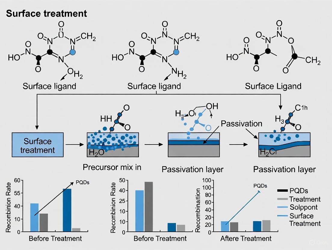
Advanced Surface Treatments and Passivation Techniques for Auger Suppression
Polar Organic Cation Engineering to Reduce Dielectric Confinement
Low-dimensional organic-inorganic hybrid perovskites, such as two-dimensional (2D) layered structures and quasi-2D systems, naturally form multi-quantum-well (MQW) structures. These structures exhibit not only quantum confinement but also a significant dielectric confinement effect. This effect arises from the substantial mismatch between the high dielectric constant of the inorganic semiconductor layers (εinorganic ≈ 6-25) and the low dielectric constant of the organic cation layers (εorganic ≈ 2-4) [4] [31]. The dielectric mismatch traps photo-generated excitons through inefficient screening of Coulomb interactions, leading to excessively large exciton binding energies (Eb) that can reach 200-470 meV in conventional 2D perovskites [4] [31]. This strong binding impedes the efficient dissociation of excitons into free carriers at room temperature (kT ≈ 26 meV), thereby reducing the quantum yield for photocurrent generation and enhancing non-radiative Auger recombination processes [4].
Polar organic cation engineering presents a powerful strategy to mitigate dielectric confinement. By incorporating organic cations with large dipole moments and higher dielectric constants, the dielectric mismatch between the organic and inorganic layers can be substantially reduced [4] [31] [32]. This enhanced screening weakens the Coulomb interaction between electrons and holes, leading to a dramatic reduction in Eb. A lower Eb facilitates more efficient exciton dissociation into free carriers, which is crucial for photovoltaic and light-emitting applications, and simultaneously suppresses Auger recombination by reducing the electron-hole wavefunction overlap [4]. This application note details the experimental protocols and material design principles for implementing this strategy, with particular emphasis on its role in reducing Auger recombination in perovskite quantum dots (PQDs) and films.
Polar Organic Cation Design Strategies
The selection and design of polar organic cations are critical for effectively reducing dielectric confinement. The following design approaches have proven successful:
Incorporating Polar Functional Groups: Introducing highly electronegative atoms or polar groups significantly increases the cation's dipole moment and dielectric constant. For instance, fluorination of phenethylammonium (PEA+) creates (S)-ortho-fluorinated-methyl-benzylamine (S-2F-MBA), which increases the organic layer's dielectric constant and reduces Eb [32]. Similarly, ethanolamine (EA+, HOCH2CH2NH3+), featuring a polar hydroxy group, possesses an exceptionally high dielectric constant of 37.7, which drastically diminishes dielectric confinement [31].
Utilizing Cations with Large Intrinsic Dipole Moments: Small cations with large permanent dipole moments, such as methylammonium (MA+, 2.3 D), can be incorporated into the inorganic cage. Their rotational freedom allows for a strong orientational polarizability, which provides additional screening of the electric field between confined charges [33].
The following table summarizes key polar organic cations and their impact on material properties.
Table 1: Properties of Selected Polar Organic Cations and Their Impact on Perovskites
| Organic Cation | Dielectric Constant (ε) | Dipole Moment (D) | Exciton Binding Energy (Eb) | Key Structural Feature |
|---|---|---|---|---|
| PEA+ [31] | ~3.3 [31] | 1.28 D [4] | ~250 meV [31] | Conventional, low-polarity cation |
| p-FPEA+ [4] | Information Missing | 2.39 D [4] | Several times smaller than PEA+ [4] | Fluorinated aromatic ring |
| S-2F-MBA+ [32] | Information Missing | Information Missing | Significantly reduced vs. non-fluorinated [32] | Fluorinated chiral cation |
| EA+ (HOCH2CH2NH3+) [31] | 37.7 [31] | Information Missing | ~13 meV [31] | Polar hydroxy group |
| Methylammonium (MA+) [33] | Information Missing | 2.3 D [33] | Anomalous QCSE response [33] | Small, rotatable dipolar cation |
The logical relationship between cation properties, the resulting material structure, and the final device performance is outlined below.
Figure 1: Logic of how polar organic cation engineering mitigates Auger recombination and improves device performance.
Quantitative Data on Performance Enhancement
Engineering polar organic cations directly translates to enhanced material properties and device performance. The reduction in Eb through mitigated dielectric confinement is the most critical outcome.
Table 2: Experimental Performance Metrics Enabled by Polar Organic Cations
| Material System | Key Performance Metric | Reported Value | Comparison / Notes |
|---|---|---|---|
| p-FPEA2MAn-1PbnBr3n+1 [4] | Auger Recombination Rate | >1-order magnitude lower | Compared to PEA+ analogue |
| p-FPEA2MAn-1PbnBr3n+1 [4] | LED Peak EQE / Luminance | 20.36% / 82,480 cd m⁻² | Suppressed efficiency roll-off |
| 2D_EA Perovskite(HOCH2CH2NH3)2PbI4 [31] | Exciton Binding Energy (Eb) | ~13 meV | Vs. 250 meV for 2D_PEA perovskite |
| 2D_EA Perovskite [31] | Free Carrier Generation | 3x higher PA signal intensity | From fs-TA measurements vs. 2D_PEA |
| S-2F-MBA cOIHP [32] | Photocurrent Density (for OER) | 4.6 mA cm⁻² | Vs. 3.35 mA cm⁻² for S-MBA cOIHP |
| S-2F-MBA cOIHP [32] | Operational Stability | 6 hours (280% extension) | In polar electrolyte vs. non-fluorinated |
Experimental Protocols
Synthesis of Fluorinated Cation-Based Perovskite Films
This protocol describes the synthesis of quasi-2D perovskite films using fluorinated organic cations, such as p-FPEA+ or S-2F-MBA+, adapted from methods in the literature [4] [32].
- Primary Reagents: Lead(II) bromide (PbBr₂, >99.99%), methylammonium bromide (MABr, >99.5%), p-fluorophenethylammonium bromide (p-FPEABr, >99%), or other fluorinated ammonium salts. Dimethylformamide (DMF, anhydrous) and dimethyl sulfoxide (DMSO, anhydrous) as solvents.
- Procedure:
- Precursor Solution Preparation: Prepare a 1.0 M precursor solution in a mixture of DMF:DMSO (4:1 v/v). For a typical p-FPEA2MA1Pb2Br7 (n=2) formulation, stoichiometrically weigh p-FPEABr, MABr, and PbBr₂ to achieve the desired molar ratio (e.g., 2:1:2). Dissolve the powders in the solvent mixture.
- Stirring and Filtration: Stir the mixture at 60°C for 4-6 hours until a clear, homogeneous solution is obtained. Filter the solution through a 0.22 μm PTFE syringe filter to remove any undissolved particles or contaminants.
- Film Deposition: Deposit the filtered solution onto the target substrate (e.g., FTO, ITO, or quartz) via a one-step spin-coating process. A typical two-step spin-coating program is 1000 rpm for 10 s (spread step) followed by 4000 rpm for 30 s (thinning step).
- Crystallization Induction: During the second spin-coating step, 10 seconds before the end of the program, drop-cast 100 μL of anhydrous chlorobenzene (CB) or diethyl ether (anti-solvent) onto the center of the spinning substrate to induce instantaneous crystallization.
- Annealing: Immediately transfer the wet film to a hotplate and anneal at 70°C for 5 minutes, then at 100°C for 15 minutes to remove residual solvent and improve crystallinity.
Characterization of Exciton Binding Energy (Eb)
Accurate determination of the Eb is crucial for validating the success of dielectric confinement reduction. The temperature-dependent photoluminescence (PL) method is widely used.
- Equipment: Cryostat system with temperature control (4-400 K), continuous-wave laser source (e.g., 405 nm), spectrometer with a CCD detector, and a calibrated power meter.
- Procedure:
- Sample Loading: Mount the perovskite film in the cryostat under a vacuum to prevent condensation and frost formation at low temperatures.
- PL Data Acquisition: Cool the sample to a low starting temperature (e.g., 20 K). Excite the sample with a low-intensity laser beam to avoid heating and record the steady-state PL spectrum. Repeat this measurement while gradually increasing the temperature in fixed increments (e.g., 10-20 K) up to room temperature (300 K) or beyond.
- Data Analysis: Integrate the area under the PL curve for each temperature to obtain the integrated PL intensity (I_PL(T)).
- Fitting with Arrhenius Equation: Fit the temperature-dependent IPL(T) data using the following modified Arrhenius equation to account for both exciton dissociation and non-radiative recombination: IPL(T) = I₀ / [1 + Aexp(-Eb/kBT) + Bexp(-Ea/kBT)] where I₀ is the intensity at 0 K, A and B are pre-exponential factors, Eb is the exciton binding energy, Ea is the activation energy for non-radiative recombination, and kB is the Boltzmann constant. The value of Eb extracted from this fitting is a reliable measure of the strength of the dielectric and quantum confinement [31].
Femtosecond Transient Absorption (fs-TA) Spectroscopy
This protocol assesses exciton dissociation and free carrier generation dynamics, providing indirect evidence of low Eb [31].
- Equipment: Femtosecond laser amplifier, optical parametric amplifier (OPA), pump-probe spectrometer with a delay stage, and a sensitive detector.
- Procedure:
- Sample Preparation: Use a high-quality, solid thin film on a transparent substrate (e.g., quartz).
- Pump-Probe Setup: Set the pump pulse energy to a low fluence (e.g., <10 μJ/cm²) to minimize multi-exciton generation. The pump wavelength should be tuned above the bandgap (e.g., 330 nm). A white-light continuum probe pulse is used to monitor changes in absorption across the visible and NIR spectrum.
- Data Collection: Record the differential transmission (ΔT/T) or absorption (ΔA) spectra at various time delays between the pump and probe pulses (from sub-ps to ns).
- Kinetic Analysis: Identify the ground-state bleach (GSB), stimulated emission (SE), and photo-induced absorption (PA) features. A more intense and longer-lived PA signal in the NIR region, assigned to free carriers, indicates more efficient exciton dissociation, a signature of low Eb [31].
The workflow for synthesizing and characterizing these advanced materials is summarized in the following diagram.
Figure 2: Experimental workflow for synthesizing and characterizing polar cation-engineered perovskites.
The Scientist's Toolkit: Research Reagent Solutions
Table 3: Essential Reagents and Materials for Polar Cation Engineering
| Reagent/Material | Function/Application | Example Purity / Specification |
|---|---|---|
| p-Fluorophenethylammonium Bromide (p-FPEABr) | High-dipole organic cation for Eb reduction [4] | >99.0% (HPLC) |
| (S)-ortho-fluorinated-methyl-benzylamine (S-2F-MBA) | Chiral, fluorinated cation for spin-dependent electronics [32] | >99.0% (Chiral HPLC) |
| Ethanolammonium Iodide/Bromide | High-ε organic cation for extreme dielectric screening [31] | >98.0% |
| Lead(II) Bromide (PbBr₂) | Metal halide precursor for inorganic framework | >99.99% (Trace Metals Basis) |
| Anhydrous N,N-Dimethylformamide (DMF) | High-quality solvent for precursor preparation | Anhydrous, 99.8% |
| Anhydrous Dimethyl Sulfoxide (DMSO) | Co-solvent for perovskite precursor inks | Anhydrous, ≥99.9% |
| Anhydrous Chlorobenzene | Anti-solvent for crystallization during spin-coating | Anhydrous, 99.8% |
The strategic engineering of polar organic cations is a highly effective method for reducing the detrimental dielectric confinement in low-dimensional perovskites. By selecting cations with high dipole moments and dielectric constants, such as fluorinated aromatics or molecules with polar hydroxy groups, researchers can dramatically lower exciton binding energies. This suppression enhances exciton dissociation, improves charge transport, and crucially, mitigates Auger recombination by reducing electron-hole wavefunction overlap. The protocols outlined herein provide a reliable roadmap for synthesizing and characterizing these advanced materials, paving the way for the development of high-performance perovskite optoelectronic devices, including brighter, more efficient LEDs and stable solar cells.
Molecular Passivation Strategies for Defect Mitigation and Trap State Reduction
Molecular passivation has emerged as a critical strategy for mitigating defects and reducing trap states in perovskite quantum dots (PQDs) and thin films, directly addressing the challenge of non-radiative Auger recombination that plagues advanced optoelectronic devices. By strategically applying organic and inorganic molecules to passivate surface defects, researchers have achieved remarkable improvements in both the efficiency and operational stability of perovskite-based solar cells. This document provides a comprehensive overview of recent advances in molecular passivation techniques, with particular emphasis on their role in suppressing Auger recombination through targeted surface treatment. We present systematically organized quantitative data, detailed experimental protocols, and key reagent information to equip researchers with practical tools for implementing these strategies in their own laboratories, ultimately contributing to the development of more efficient and stable perovskite optoelectronic devices.
Molecular Passivation Mechanisms and Quantitative Outcomes
Key Passivation Strategies and Performance Metrics
Molecular passivation functions through several complementary mechanisms to reduce defect states and suppress Auger recombination in PQDs. The table below summarizes four prominent strategies, their molecular mechanisms, and resulting performance improvements.
Table 1: Molecular Passivation Strategies for Defect Mitigation in Perovskite Materials
| Passivation Strategy | Molecular Mechanism | Performance Improvement | Impact on Auger Recombination |
|---|---|---|---|
| Extended π-Conjugation [34] | Suppresses molecular desorption, improves energy-level alignment, enhances radical-cation stability | Efficiency increased from 22.7% to 24.6%; Retention improved from 61% to 85% after 1000h illumination | Reduced trap-assisted Auger recombination via enhanced surface defect passivation |
| Core-Shell PQDs [35] | Epitaxial compatibility with host perovskite matrix passivates grain boundaries and surface defects | PCE increased from 19.2% to 22.85%; Voc from 1.120V to 1.137V; >92% retention after 900h | Suppressed non-radiative recombination through defect neutralization |
| Dual-Molecular Passivation [36] | Combined defect passivation (thiophene-based) and hole-blocking (piperazine-based) functionality | Champion device efficiency >25%; >85% retention after 600h at 50°C | Targeted mitigation of interfacial recombination pathways |
| Multi-step Diffusion Optimization [37] | Optimized doping profiles and enhanced interfacial charge transfer kinetics | PCE increased from 23.29% to 23.54%; IQE improved from ~80-95% in UV range | Reduced non-radiative Auger recombination in n-type emitter |
Quantitative Analysis of Passivation Efficacy
The effectiveness of molecular passivation strategies can be quantitatively assessed through various photovoltaic and material parameters. The following table compares key metrics before and after implementation of different passivation approaches.
Table 2: Quantitative Performance Metrics of Passivation Strategies
| Parameter | Pre-Passivation | Post-Passivation | Passivation Method |
|---|---|---|---|
| Power Conversion Efficiency (%) | 22.7 [34] | 24.6 [34] | BTBTAI with extended π-conjugation |
| Open-Circuit Voltage (V) | 1.120 [35] | 1.137 [35] | Core-shell PQD integration |
| Short-Circuit Current Density (mA/cm²) | 24.5 [35] | 26.1 [35] | Core-shell PQD integration |
| Fill Factor (%) | 70.1 [35] | 77.0 [35] | Core-shell PQD integration |
| Efficiency Retention (%) | 61 [34] | 85 [34] | BTBTAI after 1000h illumination |
| Internal Quantum Efficiency (%) | ~80 [37] | ~95 [37] | Multi-step diffusion optimization |
| Carrier Lifetime (µs) | 40 [37] | 68 [37] | Multi-step diffusion optimization |
Experimental Protocols for Molecular Passivation
Protocol 1: π-Conjugated Molecular Passivation for Perovskite Films
Principle: Organic molecules with extended π-conjugation systems suppress desorption from perovskite surfaces during processing, improving energy-level alignment and enhancing radical-cation stability for superior defect passivation and hole extraction [34].
Materials:
- Formamidinium lead iodide (FAPbI₃) perovskite precursors
- 2-(3-ethylamine)benzothieno[3,2-b]benzothiophene hydroiodide (BTBTAI) or similar π-conjugated molecules
- Dimethylformamide (DMF) and dimethyl sulfoxide (DMSO) solvents
- Chlorobenzene antisolvent
- Substrates with electron transport layer (e.g., TiO₂-coated FTO)
Procedure:
- Prepare perovskite precursor solution containing FAPbI₃ in DMF:DMSO (4:1 volume ratio)
- Add BTBTAI passivation molecule at 0.5-1.5 mol% concentration relative to Pb²⁺ content
- Stir the solution at 60°C for 4 hours until fully dissolved
- Spin-coat the solution onto substrates at 4000 rpm for 30 seconds
- During the last 5 seconds of spin-coating, apply chlorobenzene antisolvent dropwise
- Anneal at 100°C for 45 minutes in nitrogen atmosphere
- Characterize film quality using photoluminescence spectroscopy and X-ray diffraction
Validation Metrics:
- Measure efficiency retention after 1000 hours of continuous illumination
- Quantify trap state density using thermal admittance spectroscopy
- Assess molecular desorption resistance through temperature-programmed desorption
Protocol 2: In Situ Core-Shell Perovskite Quantum Dot Passivation
Principle: Core-shell structured PQDs composed of MAPbBr₃ cores and tetraoctylammonium lead bromide shells incorporated during antisolvent-assisted crystallization enable epitaxial passivation of grain boundaries and surface defects [35].
Materials:
- Methylammonium lead bromide (MAPbBr₃) core precursors
- Tetraoctylammonium bromide (t-OABr) shell precursors
- Oleylamine and oleic acid ligands
- Dimethylformamide (DMF) and toluene solvents
- Isopropanol purification solvent
- Perovskite precursor solution (1.6 M PbI₂, 1.51 M FAI, 0.04 M PbBr₂, 0.33 M MACl, 0.04 M MABr)
Procedure: A. Core-Shell PQD Synthesis:
- Dissolve 0.16 mmol MABr and 0.2 mmol PbBr₂ in 5 mL DMF with continuous stirring
- Add 50 µL oleylamine and 0.5 mL oleic acid to form core precursor solution
- Prepare separate shell precursor solution with 0.16 mmol t-OABr in DMF
- Heat 5 mL toluene to 60°C in oil bath with continuous stirring
- Rapidly inject 250 µL core precursor into heated toluene
- Immediately inject controlled amount of t-OABr-PbBr₃ shell precursor
- Allow reaction to proceed for 5 minutes until green color appears
- Centrifuge at 6000 rpm for 10 minutes, discard precipitate
- Recentrifuge supernatant with isopropanol at 15,000 rpm for 10 minutes
- Redisperse final precipitate in chlorobenzene at 15 mg/mL concentration
B. Solar Cell Fabrication with PQD Integration:
- Clean FTO substrates sequentially with soap solution, distilled water, ethanol, and acetone
- UV-ozone treatment for 15 minutes followed by preheating at 450°C for 30 minutes
- Deposit compact TiO₂ layer via spray pyrolysis
- Spin-coat mesoporous TiO₂ layer at 4000 rpm for 30 seconds followed by annealing
- Deposit perovskite film with PQD incorporation during antisolvent step
- Complete device with hole transport layer and electrode deposition
Quality Control:
- Verify PQD size distribution using transmission electron microscopy
- Confirm core-shell structure through high-resolution TEM and elemental mapping
- Assess defect passivation effectiveness via photoluminescence quantum yield measurements
Figure 1: Experimental workflow for core-shell perovskite quantum dot synthesis and device integration, illustrating key steps in creating passivated perovskite solar cells with reduced defect states.
Protocol 3: Dual-Molecular Passivation for Inverted Perovskite Solar Cells
Principle: Combination of cyclic-structured amine salts with complementary functionalities—conjugated molecules (benzene-, thiophene-based) for defect passivation and piperazine-based molecules for hole-blocking—enables simultaneous interface defect mitigation and charge carrier management [36].
Materials:
- Piperazine iodide and thiophene iodide salts
- Isopropanol solvent for passivation solution
- Pre-formed perovskite films on SAM-modified ITO substrates
- C60 or PCBM electron transport layers
- Bathocuproine (BCP) buffer layer material
- Metal electrode materials (Cu, Ag, or Au)
Procedure:
- Prepare individual 1 mM solutions of piperazine iodide and thiophene iodide in isopropanol
- Mix the solutions at 1:1 volume ratio for bimolecular passivation treatment
- Fabricate inverted (p-i-n) perovskite solar cells with self-assembled monolayer (SAM) bottom contact
- After perovskite film deposition and annealing, spin-coat the dual-molecule passivation solution at 3000 rpm for 30 seconds
- Anneal at 80°C for 5 minutes to remove residual solvent
- Deposit C60 or PCBM electron transport layer via spin-coating or thermal evaporation
- Add BCP buffer layer (8-10 nm) via thermal evaporation
- Complete device with metal electrode deposition (80-100 nm)
Characterization:
- Analyze quasi-Fermi level splitting (QFLS) and surface photovoltage (SPV) using absolute photoluminescence and Kelvin probe measurements
- Perform impedance spectroscopy to assess charge transfer kinetics
- Conduct operational stability tests using ISOS-L-1 protocol (continuous illumination at 50°C)
The Scientist's Toolkit: Essential Research Reagents
Table 3: Key Reagents for Molecular Passivation Research
| Reagent | Function | Application Context |
|---|---|---|
| BTBTAI [34] | Extended π-conjugation passivator | Suppresses molecular desorption, enhances energy-level alignment and radical-cation stability |
| Methylammonium-tetraoctylammonium lead bromide [35] | Core-shell PQD precursor | Forms epitaxially compatible passivation quantum dots for grain boundary defect mitigation |
| Piperazine iodide [36] | Hole-blocking molecular passivator | Repels minority carriers back into perovskite bulk, improves charge transfer kinetics |
| Thiophene iodide [36] | Defect-passivating molecule | Passivates defects at grain interiors and boundaries via conjugated structure |
| Tetraoctylammonium bromide [35] | Shell precursor for PQDs | Creates protective shell around perovskite quantum dots for enhanced stability |
| Oleylamine & oleic acid [35] | Surface ligands | Controls nanoparticle growth and stabilization during PQD synthesis |
| Guanabenz acetate salt [38] | Moisture-blocking passivator | Prevents perovskite hydration, obviates anion and cation vacancies in ambient fabrication |
Mechanism Visualization: Molecular Passivation Pathways
Figure 2: Molecular passivation mechanisms and performance relationships, illustrating how different passivation strategies address specific defect types and contribute to improved device metrics including suppressed Auger recombination.
Molecular passivation strategies represent a powerful approach for mitigating defects and reducing trap states in perovskite quantum dots and thin films, directly addressing the critical challenge of Auger recombination in advanced optoelectronic devices. Through strategic application of π-conjugated molecules, core-shell quantum dot architectures, and dual-molecular passivation systems, researchers have demonstrated significant improvements in both power conversion efficiency and operational stability. The experimental protocols and reagent information provided in this document offer practical guidance for implementing these advanced techniques, enabling further innovation in surface treatment methodologies. As research progresses, the continued development of tailored molecular passivation strategies will play an essential role in achieving the full potential of perovskite-based optoelectronic devices while effectively suppressing detrimental Auger recombination processes.
Ligand Exchange Protocols for Enhanced Surface Stability and Reduced Recombination
Perovskite Quantum Dots (PQDs), particularly all-inorganic CsPbX3 (X = Cl, Br, I), have emerged as promising materials for optoelectronic applications due to their exceptional optical properties, including high photoluminescence quantum yields (PLQYs), narrow emission spectra, and widely tunable bandgaps [39]. However, their ionic crystal structure and dynamic ligand binding make them inherently susceptible to environmental degradation and internal recombination losses [40] [41]. The structural degradation of PQDs primarily occurs through two mechanisms: (1) defect formation on the surface due to ligand detachment, and (2) vacancy formation in the crystal lattice due to halide migration with low activation energy [41]. These defects act as non-radiative recombination centers, severely diminishing photoluminescence efficiency and operational stability.
Auger recombination, a three-carrier process, becomes particularly pronounced under high injection conditions or in confined nanostructures like quantum dots, leading to efficiency droop and accelerated degradation [15]. While PQDs exhibit a degree of "defect tolerance," uncontrolled surface defects and inefficient charge injection imbalance can promote non-radiative Auger processes [42] [40]. Ligand exchange serves as a critical strategy to combat these issues by passivating surface states, enhancing binding affinity, and improving carrier injection balance, thereby suppressing both Shockley-Read-Hall (SRH) and Auger recombination pathways [39] [41].
Ligand Binding Chemistry and Surface Dynamics
The surface of as-synthesized PQDs is typically capped with long-chain ligands like oleic acid (OA) and oleylamine (OAm). While essential for colloidal stability, these ligands bind dynamically and weakly to the PQD surface, creating a labile layer prone to desorption [39] [41]. This desorption creates unsaturated sites ("vacancies") on the Pb²⁺ and halide ions, which function as traps for charge carriers.
The effectiveness of a ligand is governed by its binding affinity, which is determined by the donor atom and the molecular structure. Conventional X-type ligands (e.g., OA) bind anionicly to Pb atoms, while L-type ligands (e.g., OAm) coordinate through Lewis basic donor atoms to undercoordinated surface sites [39]. The defect tolerance of lead halide perovskites is partly attributed to these binding mechanisms; however, the low formation energy of surface vacancies means that weak ligands are easily displaced. Stronger binding ligands, such as those containing thiol (-SH) or multidentate phosphine groups, form more stable complexes with surface Pb atoms, reducing the equilibrium concentration of vacancies and thus the density of trap states [41]. This direct passivation suppresses SRH recombination. Furthermore, a densely packed, stable ligand layer can mitigate ion migration—a key trigger for phase segregation and Auger recombination under electrical injection—by stabilizing the crystal lattice against degradation [40] [41].
Ligand Exchange Protocols
This section provides detailed, actionable protocols for performing ligand exchange on PQDs. The core workflow, from initial synthesis to final application, is summarized in the diagram below.
Pre-Exchange Synthesis and Purification
Protocol 1: Standard Hot-Injection Synthesis of CsPbBr₃ PQDs
- Objective: To synthesize high-quality CsPbBr₃ PQDs with initial OA/OAm capping for subsequent ligand exchange.
- Materials: Cesium carbonate (Cs₂CO₃), Lead(II) bromide (PbBr₂), 1-Octadecene (ODE, 90%), Oleic acid (OA, 90%), Oleylamine (OAm, 90%), Toluene, Methyl Acetate.
- Equipment: Three-neck flask, Schlenk line, Syringes, Heating mantle, Thermostat.
- Procedure:
- Cs-Oleate Precursor: Load 0.2 g Cs₂CO₃, 1.25 mL OA, and 10 mL ODE into a 50 mL 3-neck flask. Dry under vacuum at 120°C for 1 hour. Then, heat under N₂ to 150°C until all Cs₂CO₃ reacts, forming a clear solution.
- PbBr₂ Precursor: In a separate 100 mL 3-neck flask, load 0.138 g PbBr₂, 10 mL ODE, 1 mL OA, and 1 mL OAm. Dry under vacuum at 120°C for 1 hour.
- Injection & Reaction: Under N₂ atmosphere, raise the temperature of the PbBr₂ mixture to 180°C. Rapidly inject 1 mL of the pre-heated Cs-Oleate solution. React for 5-10 seconds.
- Quenching & Isolation: Immediately cool the reaction flask in an ice-water bath. Add 20 mL of toluene and centrifuge the crude solution at 8000 rpm for 5 minutes to remove large aggregates. Recover the supernatant.
- Precipitation & Washing: Add methyl acetate (1:1 v/v) to the supernatant to precipitate the PQDs. Centrifuge at 10,000 rpm for 10 minutes. Discard the supernatant and re-disperse the pellet in 5 mL of toluene. Repeat this washing step once more. Finally, disperse the PQDs in 5 mL of anhydrous toluene for a concentration of ~10 mg/mL.
Post-Synthesis Ligand Exchange Methodologies
Protocol 2: Thiol-Based Ligand Exchange for Enhanced Stability
- Objective: To replace native OA/OAm ligands with 2-Aminoethanethiol (AET) for superior surface passivation and stability against moisture/UV light [41].
- Principle: Thiol groups (-SH) have a strong affinity for Pb²⁺ ions, forming stable covalent bonds that resist detachment and effectively passivate surface defects.
- Materials: CsPbBr₃ PQDs in toluene (from Protocol 1), 2-Aminoethanethiol (AET), Anhydrous Dimethylformamide (DMF), Toluene, Methyl Acetate.
- Procedure:
- Ligand Solution: Prepare a 10 mM solution of AET in anhydrous DMF.
- Exchange Reaction: Add 1 mL of the purified CsPbBr₃ PQD solution to 5 mL of the AET/DMF solution under vigorous stirring. The PQDs will transfer from toluene to DMF.
- Incubation: Stir the mixture at room temperature for 2 hours.
- Washing & Isolation: Add 10 mL of toluene to the mixture, causing the PQDs to precipitate. Centrifuge at 12,000 rpm for 10 minutes. Carefully discard the supernatant containing the displaced OA/OAm ligands.
- Final Dispersion: Re-disperse the purified PQD pellet in 2 mL of anhydrous DMF. Centrifuge at low speed (3000 rpm) for 2 minutes to remove any aggregates. The stable, AET-capped PQDs are now in the supernatant.
- Expected Outcome: PLQY increases from ~22% to over 51%. The PQDs maintain >95% of initial PL intensity after 60 min water exposure or 120 min UV exposure [41].
Protocol 3: Solid-State Ligand Exchange via Cation Exchange
- Objective: To incorporate cationic metal-complex ligands into a solid-state PQD matrix, creating a bifunctional catalytic system and demonstrating a non-solution-based exchange [43].
- Principle: Cations (e.g., K⁺) in a solid-state perovskite matrix (e.g., K-PHI) can be exchanged with cationic metal complexes (e.g., LnNi²⁺) in a solvent-mediated process.
- Materials: Potassium poly(heptazine imide) (K-PHI) powder, LnNiCl₂(H₂O)ₙ complex (e.g., L = 2,2'-bipyridine), Anhydrous Dimethylformamide (DMF), Acetonitrile, Deionized Water.
- Procedure:
- Preparation: Disperse 40 mg of K-PHI powder in 1 mL of anhydrous DMF. Separately, dissolve 8 mg of the LnNiCl₂(H₂O)ₙ complex in 1 mL of DMF.
- Exchange Reaction: Combine the K-PHI dispersion and the Ni-complex solution in a sealed vial under N₂ atmosphere. Stir the mixture at room temperature for 72 hours.
- Washing: Centrifuge the mixture at 10,000 rpm for 10 minutes. Wash the resulting solid pellet sequentially with DMF, deionized water, and acetonitrile to remove excess Ni complexes and released K⁺ ions.
- Drying: Dry the final LnNi-PHI powder under vacuum at 60°C for 6 hours.
- Verification: ICP-OES confirms Ni loading of ~0.3 mmol/g. Acid treatment releases the complex, which can be identified via ¹H-NMR, confirming successful exchange [43].
Research Reagent Solutions
The table below lists key reagents essential for ligand exchange experiments in PQD research.
Table 1: Essential Research Reagents for PQD Ligand Exchange
| Reagent Name | Function & Role in Experiment |
|---|---|
| Oleic Acid (OA) / Oleylamine (OAm) | Standard X- and L-type capping ligands used in initial PQD synthesis. Their replacement is the goal of most exchange protocols. |
| 2-Aminoethanethiol (AET) | Short-chain, bidentate ligand providing strong Pb-S binding for enhanced surface passivation and stability against H₂O/UV [41]. |
| Didodecyldimethylammonium Bromide (DDAB) | Commonly used to engineer surface halide composition and passivate halide vacancies, improving luminescence and stability. |
| Potassium poly(heptazine imide) (K-PHI) | A solid-state, crystalline carbon nitride matrix used as a platform for cation exchange with metal complexes [43]. |
| Bipyridyl-based Ni complexes | Cationic metal complexes (e.g., bpyNi²⁺) used in cation exchange to create bifunctional (photo/Ni) solid catalysts [43]. |
| Anhydrous Dimethylformamide (DMF) | High-polarity solvent used to facilitate ligand exchange and stabilize polar PQDs post-exchange. |
Quantitative Analysis of Ligand Performance
The effectiveness of a ligand exchange protocol is quantified through key optical, electrical, and stability metrics. The following table compares the performance of different ligand strategies.
Table 2: Quantitative Performance Metrics of Ligand-Engineered PQDs
| Ligand Strategy / Material | PLQY (%) | Stability Retention | Key Recombination Metrics | Reference / Context |
|---|---|---|---|---|
| OA/OAm (Reference) | ~22% (Post-purification) | <50% PL after 1 hr in H₂O | High SRH recombination from surface traps | [41] |
| AET (Thiol) | >51% | >95% PL after 1 hr in H₂O / 2 hr UV | Significant suppression of SRH recombination | [41] |
| Multidentate Phosphine | >90% | >90% PL after 30 days in air | Low defect density, suppressed non-radiative decay | [39] |
| Ligand-Engineered µLED | - | - | SRH coefficient reduced by >50% in small mesas | [14] |
| K-PHI w/ bpyNi²⁺ | - | Exceptional chemical stability & recyclability in catalysis | Enhanced photo/Ni dual catalytic activity | [43] |
Integration with Device Fabrication and Recombination Analysis
The ultimate test of successful ligand exchange is its performance in functional devices. In Light-Emitting Diodes (LEDs), effective passivation directly translates to higher efficiency and brightness. For instance, proper surface treatment of AlGaInP red µLEDs via steam oxidation was shown to suppress non-radiative SRH recombination at sidewalls, a principle directly analogous to ligand passivation of PQD surfaces [14]. Analysis using the ABC model (where A=SRH, B=radiative, C=Auger recombination coefficients) allows for the quantification of recombination currents.
Ligand engineering impacts these parameters directly:
- Reduced A-coefficient: Tighter ligand binding passivates trap states, reducing SRH recombination.
- Optimized Charge Injection: A balanced, stable ligand layer promotes more efficient radiative recombination (B-coefficient) and can mitigate efficiency droop by reducing the Auger recombination (C-coefficient) under high carrier injection, a critical factor in PeLEDs [42] [15].
The journey from unstable PQDs to a high-performance device, highlighting the role of ligand exchange in suppressing recombination pathways, is illustrated below.
Ligand exchange is a transformative step in the processing of PQDs, directly targeting the core challenges of surface instability and non-radiative recombination. Moving beyond standard OA/OAm systems to engineered ligands with stronger multidentate binding, such as thiols and specific polymers, provides a direct pathway to suppress SRH and Auger recombination losses. The protocols outlined herein—ranging from solution-phase thiol exchange to solid-state cation replacement—provide a practical toolkit for researchers to enhance the optoelectronic performance and environmental resilience of PQDs. Integrating these surface treatment strategies with optimized device architectures is the key to unlocking the full commercial potential of perovskite quantum dots in next-generation LEDs, lasers, and quantum technologies.
Interface Engineering in Core/Shell PQD Structures to Control Carrier Wavefunctions
The performance of perovskite quantum dots (PQDs) in optoelectronic devices is fundamentally governed by the behavior of charge carriers within the nanostructure. Auger recombination, a non-radiative process where the energy from electron-hole recombination is transferred to a third charge carrier, is a primary loss mechanism that limits the efficiency of PQD-based light-emitting diodes (LEDs) and lasers, particularly at high excitation currents [3] [44]. The interface between the core and shell in core/shell PQDs plays a critical role in dictating the spatial profile of carrier wavefunctions, and therefore, the rate of Auger recombination. Interface engineering—the deliberate manipulation of the composition and structure of the core-shell boundary—emerges as a powerful strategy to control carrier confinement and suppress these detrimental losses [45] [3]. By moving from a sharp, abrupt interface to a smooth, compositionally graded one, it is possible to tailor the confinement potential and significantly enhance the multiexciton performance of PQDs, which is essential for their application in commercial devices [45].
Quantitative Data on Interface Engineering and Auger Recombination
The impact of interface structure on carrier dynamics can be quantitatively assessed through measurements of exciton lifetimes. The following table summarizes key lifetime data for different quantum dot structures, illustrating the effect of an alloyed interfacial layer.
Table 1: Effect of Interface Engineering on Exciton Lifetimes in Core/Shell Quantum Dots
| Quantum Dot Structure | Single-Exciton Lifetime (τX, ns) | Negative Trion Lifetime (τX-, ns) | Biexciton Lifetime (τXX, ns) | Key Observation |
|---|---|---|---|---|
| CdSe/CdS (Core/Shell, sharp interface) | 20 - 40 [3] | Not Specified | Shorter than C/A/S counterparts [3] | Auger recombination rate is significant. |
| CdSe/CdSe₀.₅S₀.₅/CdS (Core/Alloy/Shell, graded interface) | Similar to sharp interface [3] | ~2x longer than C/S [3] | ~2x longer than C/S [3] | Alloy layer suppresses Auger recombination, enhancing multiexciton lifetimes. |
Experimental Protocols for Interface Engineering and Characterization
Protocol: Synthesis of Core/Alloy/Shell PQDs with Graded Interface
This protocol outlines the procedure for creating a compositionally graded interface between the core and shell to suppress Auger recombination [45] [3].
Objective: To synthesize core/alloy/shell PQDs featuring an intermediate alloyed layer for a smooth confinement potential.
Materials:
- Core precursor solutions: (e.g., CdO, Se powder, Oleic acid, 1-Octadecene)
- Alloy layer precursors: Cation and anion precursors compatible with both core and shell materials (e.g., Cd, Se, and S precursors).
- Shell precursors: (e.g., CdS or ZnS precursors)
- Coordinating solvents: 1-Octadecene, Oleylamine.
- Inert atmosphere: Nitrogen or Argon gas.
Procedure:
- Core Synthesis: Synthesize the core PQDs (e.g., CdSe) using a standard hot-injection method. Purify and characterize the core size and concentration.
- Alloy Layer Growth: a. Redisperse the purified core PQDs in a coordinating solvent at high temperature (e.g., 300-320°C) under inert atmosphere. b. Slowly and dropwise inject a mixture of cationic and anionic precursors that will form an alloy (e.g., CdSexS1-x) onto the core seeds. The composition (x) can be controlled by the molar ratio of the chalcogen precursors. c. Maintain the reaction temperature for 10-30 minutes to allow for diffusion and formation of a graded alloy layer of the desired thickness (e.g., ~1.5 nm).
- Shell Growth: a. After alloy layer formation, initiate the growth of the outer shell (e.g., CdS) using a successive ionic layer adsorption and reaction (SILAR) method or slow continuous injection. b. Precisely control the shell thickness by monitoring the reaction time and the amount of precursor injected.
- Purification: Cool the reaction mixture and purify the resulting core/alloy/shell PQDs by centrifugation with anti-solvents (e.g., ethanol/acetone). Redisperse the final product in a non-polar solvent (e.g., toluene or hexane).
Safety Notes: All procedures must be conducted in a fume hood using standard personal protective equipment, including heat-resistant gloves and safety glasses.
Protocol: Single-Qantum-Dot Spectroscopy for Auger Recombination Evaluation
This protocol describes how to measure the effect of the core/shell interface on Auger recombination at the single-particle level [45].
Objective: To directly correlate interfacial structure with biexciton lifetimes and emission efficiency, avoiding ensemble averaging.
Materials:
- Dilute solution of core/shell or core/alloy/shell PQDs.
- Spectrally clean substrate (e.g., pristine silicon wafer).
- Single-quantum-dot spectroscopy setup, including:
- Pulsed laser source (e.g., femtosecond laser).
- Microscope objective with high numerical aperture.
- Cryostat (for low-temperature measurements, if required).
- High-sensitivity, fast-response single-photon detectors (e.g., avalanche photodiodes).
- Time-correlated single-photon counting (TCSPC) module.
- Hanbury Brown and Twiss (HBT) interferometer for second-order correlation (g²(τ)) measurements.
Procedure:
- Sample Preparation: Spin-coat a highly dilute solution of PQDs onto the substrate to ensure a surface density where individual dots are spatially isolated and can be addressed separately.
- Data Acquisition: a. Locate individual PQDs using raster scanning of the laser focus across the sample. b. For each isolated QD, record the photoluminescence (PL) intensity time trace under pulsed excitation. c. Using the HBT setup, acquire the second-order correlation function g²(τ) to confirm single-photon emission and identify biexciton (XX) and exciton (X) emission peaks via photon statistics. d. Using TCSPC, measure the PL decay lifetime for the same QD at low excitation power (to measure single-exciton lifetime, τX) and at high excitation power (to measure biexciton lifetime, τXX).
- Data Analysis: a. Calculate the ratio of τXX/τX. A higher ratio indicates suppressed Auger recombination. b. Compare the statistical distribution of τXX and the biexciton emission efficiency (derived from g²(τ) measurements) across an ensemble of single QDs for both sharp-interface and graded-interface structures.
Figure 1: Single-QD Spectroscopy Workflow for Evaluating Auger Recombination.
The Scientist's Toolkit: Essential Research Reagents and Materials
Table 2: Key Reagents and Materials for PQD Interface Engineering
| Item Name | Function/Application | Specific Example |
|---|---|---|
| Chalcogenide Precursors | Source of S/Se for core, alloy, and shell growth. | Trioctylphosphine sulfide (TOP-S), Trioctylphosphine selenide (TOP-Se) [3] |
| Cationic Precursors | Source of metal cations (Cd, Pb, Zn). | Cadmium oxide (CdO), Lead acetate (Pb(OAc)₂), Zinc stearate |
| Alloying Precursors | To create a compositionally graded interface layer. | Mixtures of TOP-S and TOP-Se, or specific single-molecule precursors like Mn(S₂CNEt₂)₂ for doped alloys [30] |
| Coordinating Ligands | Control nanocrystal growth, stabilize colloids, passivate surface. | Oleic Acid (OA), Oleylamine (OLA), Trioctylphosphine oxide (TOPO) |
| Non-Coordinating Solvents | High-temperature reaction medium. | 1-Octadecene (ODE) |
| Anti-Solvents | Purification of synthesized PQDs. | Ethanol, Acetone, Methanol |
| Dopant Precursors | Introduce magnetic ions to enable spin-exchange Auger processes. | Mn(S₂CNEt₂)₂ [30] |
Visualization of Band Alignment and Wavefunction Delocalization
The electronic structure of the core/shell system is critical for understanding carrier behavior. The following diagram illustrates how different interface types affect the confinement potential and carrier wavefunctions.
Figure 2: Band Alignment and Wavefunction Effects of Interface Engineering. A graded interface softens the confinement potential, partially delocalizes the hole wavefunction, and reduces electron-hole wavefunction overlap, leading to suppressed Auger recombination.
Dielectric Screening Approaches via Shell Composition and Dimensionality Control
Dielectric screening is a critical physical phenomenon that directly influences the Coulomb electron-hole interaction within semiconductor nanomaterials. In the context of perovskite quantum dots (PQDs), effective dielectric screening reduces the undesirable non-radiative pathway known as Auger recombination, where the energy from one recombining electron-hole pair is transferred to another carrier instead of being emitted as light. This process is a major factor in the efficiency roll-off observed in PQD-based light-emitting diodes (PeLEDs) at high current densities, limiting their brightness and practical application [4]. The fundamental principle involves manipulating the nanostructure's composition and physical dimensions to enhance dielectric screening, thereby weakening the strong Coulomb interactions that lead to rapid Auger recombination.
The effectiveness of dielectric screening is intrinsically linked to the exciton binding energy (E₆). In strongly confined systems such as quasi-2D perovskites, rapid Auger recombination is directly proportional to the materials' E₆ [4]. Theoretical and experimental studies have established that the Auger recombination rate is proportional to the third power of the E₆ in strongly confined 1D material, a relationship that also applies to quasi-2D perovskites [4]. Consequently, reducing E₆ through enhanced dielectric screening presents a powerful strategy for suppressing Auger recombination. This can be achieved through two primary approaches: (1) Shell composition engineering involving the use of high-polarity molecules or core/shell structures, and (2) Dimensionality control through precise manipulation of the core/shell geometry.
Theoretical Foundations of Dielectric Screening
Fundamental Principles and Relationship to Auger Recombination
Auger recombination represents a non-radiative process involving three carriers, where an electron and hole recombine and transfer their energy to a third carrier (either an electron or hole), which subsequently relaxes back to its band edge through phonon emission. This process becomes particularly detrimental at high carrier densities, common in electroluminescent devices and under high-intensity photoexcitation. The Auger recombination rate ((k{\text{Auger}})) exhibits a cubic dependence on carrier density ((n)), expressed as (k{\text{Auger}} = C n^3), where (C) is the Auger recombination coefficient [4].
Dielectric screening directly modulates the strength of Coulomb interactions ((Vc)) responsible for Auger recombination through the relation (Vc \propto 1/(\epsilon r)), where (\epsilon) is the dielectric constant of the material and (r) is the distance between charges. In nanostructured materials, the effective dielectric constant is influenced by both the core material and the surrounding medium or shell. Enhanced dielectric screening reduces the Coulomb interaction, leading to a direct suppression of the Auger recombination rate. Research on CdSe/CdS core/shell quantum dots has demonstrated that geometry-dependent dielectric screening allows for tuning Auger recombination rates by approximately one order of magnitude [46].
Exciton Binding Energy and Dielectric Confinement
Quasi-2D perovskites exhibit self-assembled multiple-quantum-well structures characterized by strong quantum and dielectric confinement. The dielectric confinement arises from the dielectric constant mismatch between the inorganic well and surrounding organic ligands, which are less polar [4]. This dielectric mismatch additionally strengthens the E₆, making excitons more susceptible to Auger recombination. The large E₆ in quasi-2D perovskites (e.g., 470 meV for BA₂PbI₄ perovskite) contributes significantly to their rapid Auger recombination rates [4].
Table 1: Key Parameters Affecting Auger Recombination in Quantum-Confined Structures
| Parameter | Effect on Auger Recombination | Experimental Tuning Range |
|---|---|---|
| Exciton Binding Energy (E₆) | Proportional to Auger rate; ~E₆³ dependence in confined systems | 347 meV reduction via polar organic cations [4] |
| Dielectric Constant of Shell/Barrier | Inverse relationship; higher ε reduces Coulomb interaction | >90% β/γ-phase content in PVDF composites [47] |
| Core Size (CdSe/CdS QDs) | Strong influence on biexciton QY and Auger rate | 3-7 nm core size tunes Auger rates ~10x [46] |
| Shell Thickness (CdSe/CdS QDs) | Moderate effect on Auger recombination | 4-10 monolayers with limited impact on biexciton QY [46] |
Compositional Control for Enhanced Dielectric Screening
Polar Organic Cation Engineering
The strategic incorporation of polar organic cations at the A-site of quasi-2D perovskites represents a powerful approach for enhancing dielectric screening. A notable example involves replacing traditional phenethylammonium (PEA+) with p-fluorophenethylammonium (p-FPEA+) [4]. The electron-withdrawing fluorine atom at the para-position of the phenyl group polarizes the electronic state of p-FPEA+, inducing a strong molecular dipole moment of 2.39 D compared to 1.28 D for PEA+ [4]. This increased dipole moment facilitates charge separation, leading to higher effective dielectric constants that reduce the dielectric constant mismatch between organic and inorganic layers.
Protocol 3.1: Synthesis of p-FPEA-based Quasi-2D Perovskite Films
- Precursor Preparation: Dissolve stoichiometric ratios of PbBr₂, MABr (methylammonium bromide), and p-FPEABr in dimethylformamide (DMF) at a concentration of 0.8 M.
- Solution Formulation: Adjust the molar ratio of p-FPEABr: MABr: PbBr₂ to achieve the desired phase purity and dimensionality (n-value).
- Film Deposition: Spin-coat the precursor solution onto pre-cleaned substrates at 4000 rpm for 30 seconds in a nitrogen-filled glovebox.
- Annealing Process: Immediately transfer the film to a hotplate and anneal at 80°C for 10 minutes to facilitate crystallization.
- Passivation Treatment: For enhanced performance, apply a molecular passivation agent (e.g., trioctylphosphine oxide) via spin-coating to suppress non-radiative recombination at grain boundaries.
The implementation of p-FPEA+ in quasi-2D perovskites (p-FPEA₂MAₙ₋₁PbₙBr₃ₙ₊₁) results in several times smaller E₆ compared to PEA+ analogs, as confirmed by temperature-dependent photoluminescence measurements [4]. This reduction in E₆ directly correlates with a decrease in Auger recombination rate by more than one order of magnitude, significantly suppressing efficiency roll-off in resulting PeLEDs.
Dielectric Composite Engineering
An alternative approach involves creating organic-inorganic composites where perovskite quantum dots are embedded within high-dielectric-constant polymer matrices. The PVDF/APTES@CsPbBr₃ composite demonstrates this strategy effectively, where APTES-passivated CsPbBr₃ QDs are uniformly dispersed within a PVDF matrix via controlled in-situ synthesis [47]. This composite design achieves dual enhancements by triggering pronounced polar-phase crystallization (>90% β/γ-phase content) in PVDF to amplify dipole polarization while suppressing leakage pathways through QD-induced nano-confinement effects [47].
Protocol 3.2: In Situ Synthesis of PVDF/APTES@CsPbBr₃ Composites
- QD Precursor Preparation: Dissolve CsBr (0.2 mmol) and PbBr₂ (0.2 mmol) in 5 mL of DMF/DMSO mixed solvent (9:1 v/v ratio).
- Surface Functionalization: Add 50 µL of APTES (3-aminopropyl-triethoxysilane) to the precursor solution under vigorous stirring for 30 minutes.
- Polymer Matrix Preparation: Dissolve PVDF (MW = 18,000 g mol⁻¹) in the same DMF/DMSO solvent system at 10% w/v concentration.
- In Situ Composite Formation: Combine the functionalized QD precursor and PVDF solution, then initiate antisolvent-triggered crystallization by adding toluene under continuous stirring.
- Film Fabrication: Cast the composite solution onto glass substrates and dry at 80°C for 2 hours to form uniform dielectric films.
The PVDF/APTES@CsPbBr₃ composite exhibits remarkable dielectric properties, including an energy storage density of 13.69 J/cm³ at 470 kV/mm with ultrahigh efficiency of 85.03% [47]. This approach not only enhances dielectric screening but also provides temperature-stable ultraviolet fluorescence, enabling real-time self-diagnosis of thermal degradation in optoelectronic devices.
Dimensionality Control for Optimal Screening
Core/Shell Geometry Engineering
In colloidal quantum dot systems, geometry-dependent dielectric screening provides a powerful mechanism for controlling Auger recombination. Research on CdSe/CdS core/shell QDs demonstrates that both core size and shell thickness can be independently tuned to manipulate Auger recombination rates of negative and positive trions—the fundamental Auger pathways governing multi-carrier recombination [46]. Surprisingly, for certain geometric structures, Auger recombination of positive trions can become significantly slower than that of corresponding negative trions, challenging conventional understanding of II-VI quantum dots [46].
Table 2: Geometry-Dependent Auger Recombination in CdSe/CdS Core/Shell QDs
| Structural Parameter | Effect on Negative Trion Auger | Effect on Positive Trion Auger | Optimal Configuration |
|---|---|---|---|
| Core Size Increase | Reduces rate by ~3x (3 to 7 nm) | Reduces rate by ~5x (3 to 7 nm) | Larger cores (>5 nm) for balanced trion rates |
| Shell Thickness Increase | Moderate reduction (~1.5x for 4-10 ML) | Minimal effect | Thicker shells (8-10 ML) for negative trion control |
| Dielectric Constant Ratio | Inverts trion rate preference at specific εₛₕₑₗₗ/εₛₕₑₗₗ | Enables positive trion to become slower | Tailored core/shell dielectric mismatch |
Protocol 4.1: Synthesis of CdSe/CdS Core/Shell QDs with Controlled Geometry
- Core Synthesis: Prepare CdSe cores of varying sizes (3-7 nm) through hot-injection methods using cadmium oleate and trioctylphosphine selenide precursors at 300°C.
- Size Separation: Perform size-selective precipitation to obtain monodisperse core populations with specific absorption peaks (e.g., 530-620 nm).
- Shell Growth: Employ successive ionic layer adsorption and reaction (SILAR) techniques to deposit controlled CdS shell thicknesses (4-10 monolayers).
- Reaction Monitoring: Use absorption spectroscopy after each monolayer addition to monitor shell growth and maintain stoichiometric balance.
- Post-Synthesis Treatment: Purify QDs through multiple precipitation/redispersion cycles and characterize structural properties using TEM, XRD, and elemental analysis.
The dielectric screening effect in core/shell QDs arises from the redistribution of the electric field and Coulomb potential due to the dielectric contrast between core, shell, and surrounding medium. Theoretical calculations confirm that geometry-dependent dielectric screening enables independent tuning of both fundamental Auger recombination channels by approximately one order of magnitude [46]. This tunability is crucial for applications requiring specific Auger characteristics, such as high-power light-emitting diodes, lasers, and quantum light sources.
Dimensionality Control in Quasi-2D Perovskites
In quasi-2D Ruddlesden-Popper perovskites with general formula (RNH₃)₂(A)ₙ₋₁BₙX₃ₙ₊₁, the dimensionality parameter (n-value) critically influences dielectric confinement and screening. While increasing n-value reduces E₆, this approach often compromises energy transfer efficiency [4]. Alternatively, manipulation of organic cations to weaken "dielectric confinement" presents a superior strategy, as it notably reduces E₆ without altering energy transfer efficiency.
The experimental workflow below illustrates the integrated approach for developing low-Auger recombination PQDs through dielectric screening control:
Characterization and Performance Metrics
Optical Characterization Techniques
Comprehensive characterization is essential for evaluating the effectiveness of dielectric screening approaches in reducing Auger recombination. The following protocols outline key experimental methods for quantifying Auger recombination rates and dielectric screening efficacy.
Protocol 5.1: Time-Resolved Photoluminescence for Auger Rate Quantification
- Sample Preparation: Deposit thin, uniform films of PQDs on quartz substrates to minimize scattering effects.
- Excitation Conditions: Use a pulsed laser source (e.g., 400 nm, 100 fs pulse width) with variable neutral density filters to control excitation density.
- Power-Dependent Measurements: Collect time-resolved photoluminescence (TRPL) decays across excitation densities spanning 3-4 orders of magnitude.
- Multi-Exponential Fitting: Analyze TRPL decays using multi-exponential fitting functions to extract fast (Auger-dominated) and slow (radiative-dominated) components.
- Carrier Density Calculation: Convert excitation power to initial carrier density using absorption cross-section at excitation wavelength.
- Auger Coefficient Extraction: Plot fast decay rate versus carrier density squared; slope yields the three-carrier Auger coefficient.
Protocol 5.2: Exciton Binding Energy Determination via Temperature-Dependent PL
- Temperature Control: Mount samples in a cryostat with precise temperature control (4-300 K range).
- Spectral Acquisition: Collect steady-state PL spectra at 5-10 K intervals with sufficient stabilization time.
- Integrated Intensity Analysis: Plot integrated PL intensity versus inverse temperature (Arrhenius plot).
- Activation Energy Extraction: Fit high-temperature region to ( I(T) = I0/(1 + A \cdot exp(-Ea/kT)) ), where ( E_a ) represents the effective E₆.
- Complementary Methods: Validate E₆ using absorption spectroscopy to resolve excitonic and band-to-band transition energies.
Performance Metrics in Optoelectronic Devices
The ultimate validation of dielectric screening efficacy comes from performance metrics in functional devices. PeLEDs incorporating p-FPEA⁺-based quasi-2D perovskites with reduced Auger recombination demonstrate exceptional characteristics, including a peak external quantum efficiency (EQE) of 20.36% and record luminance of 82,480 cd m⁻² due to suppressed efficiency roll-off [4]. Similarly, PVDF/APTES@CsPbBr₃ composites achieve unprecedented energy storage density of 13.69 J/cm³ with 85.03% efficiency [47].
Table 3: Performance Comparison of Dielectric Screening Approaches
| Material System | Key Performance Metric | Improvement Over Reference | Application Potential |
|---|---|---|---|
| p-FPEA⁺ Quasi-2D Perovskite | 20.36% EQE; 82,480 cd m⁻² luminance | >1-order magnitude lower Auger rate | High-brightness PeLEDs for displays |
| PVDF/APTES@CsPbBr₃ Composite | 13.69 J/cm³ energy density; 85.03% efficiency | Surpasses most reported PVDF composites | Energy storage capacitors; multifunctional dielectrics |
| CdSe/CdS Core/Shell QDs | Biexciton QY tuned by ~10x through core size | Independent trion rate control | Lasers, single-photon sources, super-resolution microscopy |
The Scientist's Toolkit: Research Reagent Solutions
Successful implementation of dielectric screening strategies requires specific materials and reagents with carefully controlled properties. The following table summarizes essential research reagents for investigating dielectric screening approaches in perovskite quantum dots.
Table 4: Essential Research Reagents for Dielectric Screening Studies
| Reagent/Chemical | Function/Application | Key Characteristics | Representative Examples |
|---|---|---|---|
| p-Fluorophenethylammonium Bromide (p-FPEABr) | Polar organic cation for quasi-2D perovskites | High dipole moment (2.39 D); reduces dielectric confinement | p-FPEA₂MAₙ₋₁PbₙBr₃ₙ₊₁ perovskites [4] |
| APTES (3-Aminopropyl-triethoxysilane) | Surface passivant and coupling agent | Amino functionalization; enhances interfacial compatibility | APTES@CsPbBr₃ core-shell QDs [47] |
| Poly(vinylidene fluoride) (PVDF) | High-ε polymer matrix for composites | Promotes polar β/γ-phase crystallization; ε ~ 8-12 | PVDF/APTES@CsPbBr₃ dielectric composites [47] |
| CdSe/CdS Core/Shell QDs | Model system for geometry-dependent screening | Tunable core size (3-7 nm) and shell thickness (4-10 ML) | Auger rate engineering via dielectric contrast [46] |
| Barium Titanate (BaTiO₃) | High-permittivity filler material | Extremely high dielectric constant (εᵣ > 200) | Dielectric pads for field enhancement [48] [49] |
Dielectric screening approaches via shell composition and dimensionality control represent a powerful paradigm for addressing the critical challenge of Auger recombination in perovskite quantum dots. The strategic implementation of polar organic cations, dielectric composites, and precise core/shell geometry engineering enables unprecedented control over Coulomb interactions that drive non-radiative losses. These approaches have demonstrated remarkable success in enhancing device performance, particularly in achieving record-breaking brightness in PeLEDs and exceptional energy storage capacity in dielectric composites.
Future research directions should focus on expanding the library of high-polarity organic cations with optimized molecular dipole moments, developing multilayer core/shell structures with graded dielectric constants, and exploring machine learning approaches for predicting optimal dielectric screening configurations. Additionally, the integration of dielectric screening strategies with other passivation techniques may provide synergistic benefits for further suppressing Auger recombination while enhancing overall material stability. As these dielectric screening methodologies mature, they hold significant promise for enabling the next generation of high-performance optoelectronic devices, from ultra-bright displays to quantum light sources and beyond.
Troubleshooting PQD Synthesis and Film Formation for Minimal Auger Loss
Identifying and Mitigating Epitaxial Dimers and Structural Fusion Defects
Within the broader research on surface treatment for reduced Auger recombination in perovskite quantum dots (PQDs), controlling structural defects at the atomic scale is paramount. Epitaxial dimers and structural fusion defects represent two critical challenges during the synthesis and growth of high-quality quantum-confined structures. These defects act as non-radiative recombination centers, significantly enhancing Auger recombination rates which degrade optical performance and device efficiency. This application note details robust protocols for identifying and mitigating these defects, drawing on advanced principles from surface science and material engineering to enhance the photoluminescence quantum yield (PLQY) and stability of PQDs.
The following core concepts are essential for understanding the protocols outlined in this document:
- Epitaxial Dimers: A common surface defect occurring when two atoms form an undesired bond on the crystal surface during epitaxial growth, disrupting the periodic lattice structure and introducing mid-gap states that facilitate non-radiative Auger recombination.
- Structural Fusion Defects: Imperfections arising from the uncontrolled fusion or merging of adjacent quantum dots or nanocrystals, leading to the loss of quantum confinement, altered emission profiles, and increased Auger recombination losses.
Background and Significance
The optoelectronic performance of PQDs is critically dependent on their surface chemistry and structural integrity. Auger recombination, a three-carrier non-radiative process, is drastically accelerated by the presence of surface defects and traps, particularly epitaxial dimers and sites prone to structural fusion. These defects quench luminescence, reduce charge carrier lifetimes, and ultimately limit the performance of PQDs in applications such as light-emitting diodes (LEDs) and lasers. Mitigating these defects requires a multi-faceted approach involving precise control over synthesis parameters, targeted surface treatments, and rigorous characterization.
The table below summarizes the impact of these primary defects on PQD properties:
Table 1: Impact of Key Defects on PQD Properties
| Defect Type | Impact on Auger Recombination | Effect on PLQY | Influence on Stability |
|---|---|---|---|
| Epitaxial Dimers | Acts as a strong non-radiative trap, enhancing three-body carrier capture. | Significant reduction due to increased non-radiative pathways. | Can create chemically unstable surface sites, promoting degradation. |
| Structural Fusion | Increases wavefunction overlap and density of states at fusion boundaries. | Broadening and quenching of emission spectrum. | Leads to Ostwald ripening and loss of nanoscale structure over time. |
Defect Identification and Characterization Protocols
Accurate identification is the first step toward effective mitigation. The following protocols outline key methodologies for characterizing these defects.
Protocol: Spectral Analysis for Defect Identification
This protocol uses steady-state and time-resolved photoluminescence (TRPL) to probe defect states.
- Primary Objective: To identify the spectral signatures and carrier dynamics associated with epitaxial dimers and fusion defects.
- Experimental Workflow:
- Sample Preparation: Disperse the PQD sample in a non-solvent matrix (e.g., toluene for organic-capped PQDs) and drop-cast onto a clean, optically flat substrate (e.g., fused silica).
- Steady-State PL Measurement: Acquire the PL emission spectrum using a fluorometer with excitation at the band edge (e.g., 400 nm for CsPbBr₃). Note the full width at half maximum (FWHM) and any shoulder peaks or asymmetry, which indicate heterogeneous emission from defects.
- Time-Resolved PL (TRPL) Measurement: Use a time-correlated single photon counting (TCSPC) system with pulsed laser excitation. Fit the decay curve to a multi-exponential model: ( I(t) = A + \sumi Bi e^{-t/\tau_i} ).
- Data Interpretation:
- A dominant, very short lifetime component (τ₁ < 1 ns) is often indicative of non-radiative recombination at epitaxial dimers [14] [15].
- A long-tailed, multi-exponential decay is characteristic of heterogeneous recombination from a distribution of trap states, commonly found in samples with structural fusion defects.
The workflow for this spectral analysis protocol is summarized in the diagram below:
Protocol: Quantitative Recomposition Analysis via the ABC Model
This protocol quantifies the contributions of different recombination pathways, providing a quantitative measure of defect-mediated Auger recombination.
- Primary Objective: To extract the relative contributions of Shockley-Read-Hall (SRH), radiative, and Auger recombination coefficients from light output versus current density (L-J) measurements.
- Experimental Workflow:
- Device Fabrication: Fabricate an electroluminescent device from the PQD film. Alternatively, for optical pumping, prepare a dense, solid film with minimal inter-dot spacing.
- L-J Measurement: Place the sample in a calibrated integrating sphere. Measure the absolute light output power (L) as a function of injected current density (J) under pulsed conditions to minimize heating effects.
- Internal Quantum Efficiency (IQE) Extraction: Calculate the external quantum efficiency (EQE) from the L-J data. Estimate the outcoupling efficiency (ηout) to derive IQE (IQE = EQE / ηout). A typical estimate for planar films is ηout ≈ 0.2.
- ABC Model Fitting: Fit the IQE vs. carrier density (n) data to the ABC model, where the total recombination rate ( R{total} ) is given by: ( R{total} = An + Bn^2 + Cn^3 ) Here, ( A ) is the SRH coefficient (related to epitaxial dimers), ( B ) is the radiative coefficient, and ( C ) is the Auger coefficient. The IQE is given by: ( IQE = \frac{Bn^2}{An + Bn^2 + Cn^3} )
- Data Interpretation: An elevated A-coefficient signifies high defect density from dimers and surface traps. An elevated C-coefficient is strongly linked to structural fusion and loss of quantum confinement, which increases wavefunction overlap [14] [15].
Table 2: Key Parameters from ABC Model Fitting for Defect Analysis
| Recombination Coefficient | Physical Meaning | Correlation with Defect Type |
|---|---|---|
| A (SRH Coefficient) | Rate of non-radiative recombination via trap states. | Directly proportional to the density of epitaxial dimers and surface defects. |
| B (Radiative Coefficient) | Rate of bimolecular radiative recombination. | Suppressed in the presence of both dimer and fusion defects. |
| C (Auger Coefficient) | Rate of three-carrier non-radiative Auger recombination. | Sharply increases with structural fusion due to enhanced carrier-carrier interactions. |
Defect Mitigation Protocols
Once identified, targeted surface treatments are required to suppress these defects.
Protocol: Multi-Step Epitaxial Growth for Dimer Suppression
Adapted from the molecular beam epitaxy (MBE) of van der Waals materials, this protocol emphasizes separate control over nucleation and growth phases to prevent the formation of epitaxial dimers and related defects like twin domains and pyramidal growth [50].
- Primary Objective: To achieve highly crystalline, wafer-scale PQD films with a minimal density of epitaxial dimers by decoupling nucleation from coalescence.
- Experimental Workflow:
- Substrate Pre-Treatment: Clean the substrate (e.g., SiO₂/Si or glass) with oxygen plasma to ensure a uniform, hydrophilic surface with controlled wettability.
- Low-Temperature Nucleation: Deposit a thin, initial layer of the perovskite precursor (e.g., PbI₂ and CsBr) at a low substrate temperature (e.g., 50-70°C). This step ensures a high density of small, randomly oriented nuclei while suppressing the surface mobility that leads to dimer formation.
- Thermal Annealing for Coalescence: Ramp the substrate temperature to an optimal range for crystal growth (e.g., 90-110°C for all-inorganic PQDs). This provides thermal energy for the nuclei to coalesce into a continuous film, healing point defects and promoting a well-ordered lattice.
- Post-Growth Passivation: Immediately after growth, expose the film to a passivating ligand solution (e.g., Oleic Acid/Oleylamine in toluene) to terminate dangling bonds and stabilize the surface against dimer reformation.
Protocol: Steam Oxidation for Surface Passivation
Inspired by the passivation of AlGaInP micro-LEDs, this protocol uses a controlled steam oxidation process to create a thin, insulating oxide layer on the PQD surface, effectively pacifying surface states and suppressing recombination [14].
- Primary Objective: To reduce the surface recombination velocity (S) by chemically converting defective surface layers into a benign, wide-bandgap oxide shell.
- Experimental Workflow:
- Sample Activation: Place the solid PQD film in a quartz boat and pre-anneal in a dry nitrogen atmosphere at 100°C for 5 minutes to remove surface moisture.
- Steam Oxidation: Introduce steam into the reactor chamber by bubbling N₂ gas through deionized water at 90°C. Maintain the sample at a constant temperature of 300°C for a defined duration. Crucially, the optimal oxidation time is size-dependent [14]:
- For PQD arrays with ~50 nm features: 45-60 minutes.
- For PQD arrays with ~5-10 nm features: 15-30 minutes.
- Post-Oxidation Annealing: After oxidation, purge the chamber with pure N₂ and anneal the sample for an additional 10 minutes at 300°C to stabilize the newly formed oxide interface and reduce mechanical stress.
The logical relationship between defect type, mitigation strategy, and outcome is shown below:
The Scientist's Toolkit: Research Reagent Solutions
Table 3: Essential Materials for Defect Mitigation in PQDs
| Item Name | Function/Application | Example Specification |
|---|---|---|
| Cesium Lead Bromide (CsPbBr₃) Precursors | Base materials for synthesis of all-inorganic PQDs. | Cs₂CO₃ (99.9%), PbBr₂ (99.99%), sourced from Sigma-Aldrich. |
| Oleic Acid / Oleylamine Ligands | Surface passivation during synthesis to control growth and prevent fusion. | Technical Grade 90%, stored under N₂. |
| Plasma Cleaner | Substrate pre-treatment to ensure uniform nucleation and wettability. | Harrick Plasma PDC-32G. |
| Precision Tube Furnace | For controlled steam oxidation and post-growth annealing. | MTI Corporation OTF-1200X, with steam inlet. |
| Atomic Layer Deposition (ALD) System | For conformal deposition of Al₂O₃ as a final passivation layer. | Beneq TFS 200. |
| Time-Correlated Single Photon Counting (TCSPC) System | For TRPL measurements to extract carrier lifetimes and identify defects. | Horiba Scientific DeltaFlex. |
The systematic identification and mitigation of epitaxial dimers and structural fusion defects are non-negotiable for advancing the performance and commercial viability of PQDs in optoelectronic applications. The protocols detailed herein—spanning advanced spectral characterization, quantitative ABC modeling, multi-step epitaxial growth, and steam oxidation—provide a comprehensive toolkit for researchers to significantly suppress Auger recombination. Implementing these surface treatment strategies will lead to PQD materials with higher luminescent efficiency, superior stability, and ultimately, a greater potential for integration into next-generation quantum light sources and displays.
Auger recombination is a non-radiative process in semiconductors where the energy released from an electron-hole pair recombination is transferred to a third charge carrier (an electron or a hole) instead of being emitted as a photon [51] [26]. This third carrier is excited to a higher energy state within the same band and subsequently relaxes back to the band edge, releasing its excess energy as heat through phonon emissions [51]. This process represents a significant energy loss mechanism in optoelectronic devices.
The Auger recombination rate exhibits a strong dependence on carrier concentration, typically following a cubic relationship expressed as RAuger = Cn³, where C is the material-specific Auger coefficient and n represents the carrier concentration [51]. This strong dependence makes Auger recombination particularly dominant at high excitation densities, where it can outcompete radiative recombination pathways, leading to efficiency roll-off in light-emitting diodes (LEDs), reduced open-circuit voltage in solar cells, and increased thresholds for achieving optical gain in lasers [26].
In quantum-confined systems such as perovskite quantum dots (PQDs) and quasi-2D perovskites, Auger recombination is significantly enhanced due to several factors: increased Coulomb electron-hole interactions, relaxed momentum conservation requirements, and amplified local carrier densities resulting from efficient energy transfer processes [4] [24] [52]. Understanding and mitigating Auger recombination is therefore crucial for optimizing the performance of PQD-based optoelectronic devices, particularly under high excitation conditions required for applications such as lasers and high-brightness LEDs.
Quantitative Data on Auger Recombination Thresholds
The transition into Auger-dominated regimes occurs at specific excitation densities that vary significantly across different material systems. The table below summarizes key quantitative data on Auger recombination thresholds and rates from recent research:
Table 1: Auger Recombination Parameters Across Different Material Systems
| Material System | Auger Coefficient (cm⁶/s) | Excitation Density Threshold | Key Observations | Reference |
|---|---|---|---|---|
| Quasi-2D Perovskites (p-FPEA+) | Not specified | Broad range with high PLQY | Auger rate 1 order of magnitude lower than PEA+ analog; record luminance of 82,480 cd m⁻² | [4] |
| III-V Semiconductors | 10⁻²⁸–10⁻²⁹ | High injection levels | Coefficient decreases with increased band gap | [51] |
| InGaN/GaN LEDs | 1.4–2.0×10⁻³⁰ | Low current densities | Primary mechanism for efficiency droop in blue/green LEDs | [51] |
| Conductive QD Solids | Not specified | ~10⁻³ carriers per QD | Disorder creates "Auger hot spots"; faster Auger with higher mobility | [5] |
| CsPb(BrxCl1-x)3 NCs | Not specified | ASE threshold: 25 μJ cm⁻² (low defects) | Deep-level defects enhance Auger recombination | [24] |
| Self-assembled QDs | Not specified | Auger time: ~500 ns | Much slower than colloidal QDs; still quenches trion transition by ~80% | [53] |
Table 2: Impact of Material Properties on Auger Recombination
| Material Property | Impact on Auger Recombination | Experimental Evidence |
|---|---|---|
| Exciton Binding Energy (E₆) | Proportional to Auger rate; reduction suppresses Auger | p-FPEA+ quasi-2D perovskite with reduced E₆ shows 10× lower Auger rate [4] |
| Deep-Level Defects | Enhance Auger via charge separation and trion formation | Mixed halide perovskites with Cl-related defects show increased ASE thresholds [24] |
| Energy Disorder | Creates "Auger hot spots" through carrier congregation | Conductive QD solids show efficient AR at densities as low as 10⁻³ per QD [5] |
| Quantum Confinement | Increases electron-hole wavefunction overlap | Smaller QDs exhibit faster Auger recombination rates [24] |
| Dielectric Confinement | Enhances Coulomb interaction; increases Auger rate | Weakening dielectric confinement reduces Auger recombination [4] |
Experimental Protocols for Characterization
Time-Resolved Photoluminescence (TR-PL) Measurements
Purpose: To quantify carrier recombination dynamics and distinguish between radiative and non-radiative pathways.
Materials and Equipment:
- Pulsed laser source (wavelength suitable for bandgap excitation)
- Time-correlated single photon counting (TCSPC) system or streak camera
- Cryostat for temperature-dependent studies (77K to 400K)
- Monochromator or appropriate spectral filters
- Single-photon sensitive detector (PMT, APD, or SSPD)
Procedure:
- Sample Preparation: Deposit PQD films on quartz substrates with optical density 0.1-0.3 at excitation wavelength. Use inert atmosphere for sensitive materials.
- System Calibration: Measure instrument response function (IRF) using a scattering solution or reference dye. Ensure IRF width < 2% of measured lifetimes.
- Data Acquisition: Excite samples at various fluences (0.1-100 μJ/cm²) and collect decay curves at the PL peak wavelength. Use low repetition rate lasers (<1 MHz) or appropriate neutral density filters to avoid pile-up effects.
- Multi-exponential Fitting: Fit decay curves to I(t) = ΣAᵢexp(-t/τᵢ) where Aᵢ are amplitudes and τᵢ are decay times.
- Carrier Density Calculation: Calculate initial carrier density n₀ = αF/ℏω, where α is absorption coefficient, F is fluence, and ℏω is photon energy.
- Auger Coefficient Extraction: Plot decay rate (1/τ) versus n₀². Slope provides Auger coefficient C for processes following dn/dt = -Cn³.
Interpretation: Dominant fast decay components (<100 ps) at high excitation densities typically indicate significant Auger recombination.
Transient Absorption (TA) Spectroscopy
Purpose: To directly monitor carrier densities and probe many-body interactions.
Materials and Equipment:
- Femtosecond laser system (Ti:Sapphire amplifier with OPA)
- Pump-probe spectrometer with mechanical delay stage
- White light continuum generation setup
- Multichannel spectrometer with array detector
- Closed-cycle cryostat for temperature control
Procedure:
- Sample Preparation: Prepare optically uniform PQD films with OD ~0.3-0.6 at excitation wavelength in inert environment.
- Spectral Characterization: Record ground-state absorption spectrum prior to TA measurements.
- Pump-Probe Measurements: Excite samples with pump pulses and probe with delayed white light continuum. Monitor photoinduced absorption (PIA) and photobleaching (PB) features.
- Excitation Density Series: Collect TA data at multiple pump fluences (101²-101⁵ photons/cm²/pulse).
- Global Analysis: Use target analysis or global fitting to extract species-associated spectra and decay kinetics.
- Auger Identification: Identify Auger recombination through its characteristic cubic dependence on carrier density.
Interpretation: Rapid decay of photobleaching signal that accelerates with increasing pump fluence indicates dominant Auger recombination.
Microwave Photoconductance (TRMC) Measurements
Purpose: To monitor mobile charge carrier dynamics without contacts.
Materials and Equipment:
- Microwave cavity with Q-factor > 2000
- Pulsed laser source (wavelength suitable for bandgap excitation)
- Microwave frequency source (8-12 GHz) and detection electronics
- Temperature-controlled sample mount
Procedure:
- Sample Preparation: Prepare PQD films on non-conducting substrates (quartz, sapphire).
- Cavity Calibration: Measure cavity response function and quality factor.
- Photoconductance Measurements: Monitor microwave reflectance changes following pulsed laser excitation.
- Excitation Density Variation: Measure photoconductance transients at varying excitation densities (101⁰-101³ photons/cm²/pulse).
- Mobility Extraction: Calculate carrier mobility from photoconductance amplitude.
- Lifetime Analysis: Extract carrier lifetimes from photoconductance decay.
Interpretation: Decreased photoconductance amplitude at high excitation densities indicates higher-order recombination processes like Auger recombination.
Material Design and Surface Treatment Strategies
Research Reagent Solutions for Reduced Auger Recombination
Table 3: Key Research Reagents for Suppressing Auger Recombination
| Reagent/Chemical | Function in Auger Suppression | Application Protocol |
|---|---|---|
| p-fluorophenethylammonium (p-FPEA+) | Reduces exciton binding energy via increased dielectric constant | Add during perovskite crystallization; replaces PEA+ in quasi-2D structures [4] |
| Lead Acetate Trihydrate | Provides lead-rich environment reducing halide vacancies | Use as Pb²⁺ source in synthesis; enables stoichiometric control [24] |
| DDAC (Didodecyldimethylammonium chloride) | Surface passivation ligand for PQDs | Ligand exchange process; binds to surface trap states [24] |
| MPTS ((3-Mercaptopropyl)trimethoxysilane) | Cross-linking agent for QD-graphene composites | Covalent linkage between QDs and rGO; reduces interfacial defects [13] |
| Thermal Oxidation Treatment | Reduces Z1/2 centers (carbon vacancies) in SiC | Post-growth annealing in controlled O₂ environment [15] |
| 1,2-ethanediamine (EDA) | Short ligand for enhanced inter-dot coupling | Layer-by-layer deposition with ligand exchange [5] |
Surface Passivation Techniques
Oxide-based Passivation:
- Protocol: Atomic layer deposition (ALD) of Al₂O₃ or HfO₂ at 80-150°C with thickness 2-10 nm
- Mechanism: Reduces surface state density by terminating dangling bonds
- Optimization: Use multiple ALD cycles with purging steps between precursor exposures
Organic Ligand Engineering:
- Protocol: Post-synthetic ligand exchange using ammonium halides or thiols
- Mechanism: Passivates surface traps and modulates dielectric environment
- Optimization: Use ligand solutions in apolar solvents with 24-48 hour exchange time
Hybrid Passivation:
- Protocol: Sequential application of organic ligands followed by inorganic shells
- Mechanism: Combines benefits of both approaches for enhanced stability
- Optimization: Precisely control shell thickness to maintain quantum confinement while reducing surface states
Workflow and Pathway Diagrams
Auger Recombination Mechanisms Diagram
Experimental Optimization Workflow Diagram
Optimizing excitation density thresholds to avoid Auger-dominated regimes requires a multi-faceted approach combining material design, surface treatment, and precise characterization. Key implementation guidelines include:
Material Selection Criteria:
- Choose organic cations with high dipole moments (e.g., p-FPEA+) to reduce exciton binding energy and dielectric confinement [4]
- Implement mixed-halide compositions carefully to minimize deep-level defects while achieving target emission wavelengths [24]
- Utilize short conductive ligands (e.g., EDA, BDA) in QD solids to balance mobility enhancement against Auger recombination promotion [5]
Characterization Best Practices:
- Employ multiple complementary techniques (TR-PL, TA, TRMC) to cross-validate Auger recombination parameters
- Always perform excitation density-dependent studies to identify transition points into Auger-dominated regimes
- Include temperature-dependent measurements to distinguish between different recombination pathways
Threshold Optimization Strategies:
- Target excitation densities below 10⁻³ carriers per QD in conductive QD solids to avoid disorder-enhanced Auger recombination [5]
- For blue-emitting PQDs, aim for ASE thresholds below 25 μJ cm⁻² through defect management and surface passivation [24]
- In quasi-2D perovskites for LEDs, focus on reducing Eb to suppress efficiency roll-off while maintaining high PLQY through simultaneous defect passivation [4]
By systematically applying these protocols and design principles, researchers can effectively push the operational thresholds of PQD-based devices into regimes where radiative processes dominate, enabling higher efficiency and performance for optoelectronic applications.
Addressing Charge Imbalance and Trion-Induced Auger Recombination Channels
In quantum dot light-emitting diodes (QD-LEDs), charge imbalance—the unequal injection of electrons and holes into the quantum dot (QD) emissive layer—poses a significant challenge to device performance and stability. This imbalance often leads to the formation of trions (charged excitons), which are states where an exciton coexists with an excess charge carrier. The non-radiative Auger recombination (AR) of these trions, a process where the recombination energy is transferred to the third carrier, is a dominant loss channel that severely reduces the luminescence efficiency of QD-LEDs, particularly at high operating currents—a phenomenon known as "efficiency roll-off" [3] [54].
For perovskite quantum dots (PQDs), this issue is compounded by their intrinsic ionic nature and high defect density, which can exacerbate charge trapping and imbalance [41]. This application note, framed within a broader thesis on surface treatment for reduced Auger recombination in PQDs, details the characterization of trion-induced losses and provides targeted protocols to mitigate them through advanced material engineering and device optimization. The goal is to equip researchers with methodologies to enhance the performance and stability of next-generation optoelectronic devices.
Background and Key Challenges
Auger recombination is a non-radiative process in which an electron and a hole recombine and transfer their energy to a third charge carrier (an additional electron or hole), which subsequently thermalizes, converting the energy to heat [3]. In the specific case of a negative trion (X⁻), which consists of two electrons and one hole, the Auger process results in a hot electron, greatly reducing the luminescence quantum yield [54].
The impact of this process is particularly severe in conductive QD solids, where energy disorder causes charge carriers to congregate in low-energy sites, creating "Auger hot spots." This congregation makes AR the dominant decay path even at very low excitation densities (as low as 10⁻³ per QD) [55]. Furthermore, in strongly confined systems like quasi-2D perovskites, a high exciton binding energy (E₆) amplifies the Coulomb electron-hole interaction, accelerating the Auger recombination rate, which is theoretically proportional to the third power of E₆ [4].
Table 1: Key Recombination Channels and Their Impact on QD-LED Performance.
| Recombination Channel | Carrier Species | Effect on Device Performance |
|---|---|---|
| Radiative Recombination | Single Exciton (X) | High-efficiency light emission; desired operational mode. |
| Auger Recombination | Negative Trion (X⁻), Biexciton (XX) | Efficiency roll-off at high currents; energy loss as heat; reduced operational lifetime. |
| Trap-Assisted Recombination | Defect-Localized Carriers | Reduced photoluminescence quantum yield (PLQY); low brightness. |
Quantitative Data and Characterization
Characterizing the dynamics of multicarrier states is essential for understanding and mitigating Auger losses. The following table summarizes key lifetime parameters for different QD structures, illustrating how engineered heterostructures can suppress Auger recombination.
Table 2: Exciton and Multiexciton Dynamics in Engineered Core/Shell QDs [3].
| QD Structure | Core/Shell Dimensions | Single-Exciton Lifetime, τₓ (ns) | Negative Trion Lifetime, τₓ⁻ (ps) | Biexciton Lifetime, τₓₓ (ps) |
|---|---|---|---|---|
| Core/Shell (C/S) | CdSe (r=1.5 nm)/CdS (H=2.0 nm) | 20 | 130 | 60 |
| Core/Shell (C/S) | CdSe (r=1.5 nm)/CdS (H=5.5 nm) | 40 | 410 | 150 |
| Core/Alloy/Shell (C/A/S) | CdSe (r=1.5 nm)/CdSe₀.₅S₀.₅ (L=1.5 nm)/CdS | ~40 | 580 | 310 |
Data from Table 2 reveal two critical strategies for suppressing Auger recombination:
- Increasing Shell Thickness: Thickening the CdS shell in C/S QDs from 2.0 nm to 5.5 nm increases the effective volume of the electron wavefunction, leading to a more than 3-fold increase in the negative trion lifetime (τₓ⁻).
- Interface Alloying: Introducing an intermediate alloyed layer (CdSe₀.₅S₀.₅) in C/A/S QDs significantly prolongs τₓ⁻ and τₓₓ compared to a pure C/S structure of similar volume. This is attributed to a "smoothing" of the confinement potential, which reduces the wavefunction overlap critical for the Auger process [3].
Experimental Protocols
Protocol: Time-Resolved Photoluminescence (TRPL) for Trion Lifetime Characterization
Objective: To measure the lifetime of neutral excitons (τₓ) and negative trions (τₓ⁻) in QD films under different charge injection conditions.
Materials:
- QD Sample: Films of core/shell or core/alloy/shell QDs (e.g., CdSe/CdS or CdSe/CdSeS/CdS).
- Optical Cryostat: For temperature-controlled measurements.
- TRPL Setup: Including a pulsed laser source (e.g., ~400 nm), a fast-response photodetector, and time-correlated single-photon counting (TCSPC) electronics.
- Photochemical Doping Setup: For controlled electron doping (optional) [54].
Procedure:
- Film Preparation: Deposit a thin, optically dense film of the QDs onto a clean substrate (e.g., quartz) using spin-coating or drop-casting.
- Neutral Exciton Measurement: a. Place the sample in the cryostat and cool to 10 K to suppress phonon-mediated decay. b. Excite the film with a low-fluence pulsed laser to ensure, on average, much less than one exciton per QD is generated per pulse. c. Record the PL decay curve. Fit the decay kinetics with a multi-exponential model to extract the dominant lifetime component, which corresponds to the neutral exciton lifetime (τₓ).
- Negative Trion Measurement: a. Photochemical Doping Method: Expose the QD film to a controlled environment for electron donation (e.g., sodium borohydride vapor) [54]. Alternatively, for device-relevant studies, integrate the QD film into a simple electron-only device structure. b. Under the doped conditions, repeat the low-fluence TRPL measurement. The observed significantly shortened lifetime component corresponds to the negative trion Auger lifetime (τₓ⁻).
- Data Analysis: Compare τₓ and τₓ⁻ from the same sample. A much shorter τₓ⁻ is a direct signature of efficient Auger recombination. The difference in lifetimes between different QD structures (e.g., C/S vs. C/A/S) quantifies the efficacy of the structural engineering in suppressing Auger decay.
Protocol: Fabrication of Inverted QD-LED with Balanced Charge Injection
Objective: To fabricate a QD-LED with an inverted architecture that facilitates direct charge injection and allows for the evaluation of efficiency roll-off.
Materials:
- Substrate: Patterned Indium Tin Oxide (ITO) on glass.
- Electron Transport Layer (ETL): ZnO nanoparticle colloidal solution (~50 nm).
- Emissive Layer: Solution of engineered QDs (e.g., C/A/S QDs).
- Hole Transport Layer (HTL): 4,4′-Bis(N-carbazolyl)-1,1′-biphenyl (CBP) or composite Spiro-OMeTAD with p-type QDs [56].
- Anode: MoOₓ (10 nm) / Aluminum (Al) stack.
Procedure:
- Substrate Cleaning: Clean the ITO/glass substrates sequentially in ultrasonic baths of detergent, deionized water, acetone, and isopropanol. Treat with oxygen plasma for 15 minutes.
- ETL Deposition: Spin-coat the ZnO nanoparticle solution onto the ITO cathode at 3000 rpm for 30 seconds. Anneal at 150°C for 30 minutes in air to form a compact ~50 nm thick film.
- QD Layer Deposition: a. Transfer the substrate into a nitrogen-filled glovebox. b. Spin-coat a dilute solution of the engineered QDs (e.g., C/A/S QDs) onto the ZnO layer at 2000 rpm for 40 seconds. This should form a sub-monolayer to two monolayers of QDs. c. (Optional) For surface treatment, introduce a ligand exchange step using a solution of short-chain ligands (e.g., 2-aminoethanethiol) to improve charge transport and stability [41].
- HTL and Anode Deposition: a. Thermally evaporate the CBP layer (60 nm) onto the QD layer at a rate of 0.2-0.4 Å/s under high vacuum (<5×10⁻⁶ Torr). b. Subsequently, evaporate a MoOₓ interlayer (10 nm) followed by an Al anode (100 nm) through a shadow mask.
- Device Testing: a. Encapsulate the finished device with a glass lid and epoxy resin in the glovebox. b. Characterize the current-density-voltage (J-V-L) characteristics using a source meter and a calibrated photodiode. c. Measure the external quantum efficiency (EQE) as a function of current density to quantify the efficiency roll-off. A higher roll-off onset current indicates successful suppression of Auger recombination.
The Scientist's Toolkit: Research Reagent Solutions
Table 3: Essential Materials for Investigating and Mitigating Trion-Induced Auger Recombination.
| Reagent / Material | Function / Application | Key Consideration |
|---|---|---|
| Core/Alloy/Shell (C/A/S) QDs | Model emitters with intrinsically suppressed Auger recombination for comparative studies. | The alloyed layer (e.g., CdSe₀.₅S₀.₅) smoothens the confinement potential [3]. |
| p-Fluorophenethylammonium (p-FPEA) | High-polarity organic cation for quasi-2D perovskites to reduce exciton binding energy (Eᵦ). | Lower Eᵦ leads to >1 order of magnitude reduction in Auger recombination rate [4]. |
| SnS Quantum Dots | p-Type semiconductor for constructing type-II p-n heterojunctions and composite HTLs. | Enhances built-in field, promotes charge separation, and balances electron/hole mobility [56]. |
| 2-Aminoethanethiol (AET) | Short-chain, bidentate ligand for post-synthetic surface passivation of PQDs. | Strong coordination with Pb²⁺ passivates surface defects, inhibiting non-radiative decay [41]. |
| Spiro-OMeTAD / SnS QD Composite | A high-performance hole transport layer (HTL) for efficient and balanced charge injection. | Doping with SnS QDs improves hole extraction and increases recombination resistance (Rᵣₑc) [56]. |
Visualization of Concepts and Workflows
Charge Imbalance and Trion Formation Pathway
Diagram 1: Pathway from charge imbalance to efficiency loss.
Material Engineering & Device Fabrication Workflow
Diagram 2: Experimental workflow for developing high-performance QD-LEDs.
Strategies for Controlling Phase Purity and Preventing Inefficient Energy Transfer
Perovskite quantum dots (PQDs) have emerged as a revolutionary class of semiconducting materials with exceptional optoelectronic properties, including high photoluminescence quantum yield (PLQY), tunable band gaps, and high charge carrier mobility [57] [42]. However, their path to commercial application is hampered by challenges in maintaining phase purity and minimizing inefficient energy transfer processes, which directly impact device performance and stability [42]. Inefficient energy transfer and Auger recombination, a non-radiative process where an electron-hole pair recombines and transfers its energy to another charge carrier, are particularly detrimental as they reduce light emission efficiency and overall device performance [30].
This application note outlines specific surface treatment strategies and experimental protocols to control phase purity and suppress Auger recombination in PQDs. By focusing on advanced doping techniques and ligand engineering, we provide researchers with methodologies to enhance the optical properties and stability of PQD-based materials, framed within the context of a broader thesis on surface treatment for reduced Auger recombination.
Surface Treatment Strategies and Quantitative Analysis
Energy Transfer Modulation via Nd³⁺ Doping
Experimental Context: Researchers investigated zinc borosilicate glasses co-doped with Nd³⁺ ions and CsPbBr₃ PQDs to explore energy transfer mechanisms and enhance optical properties [57].
Key Quantitative Findings: The incorporation of Nd₂O₃ at varying concentrations (0.1-0.5 mol%) demonstrated significant impacts on the structural and optical properties of CsPbBr₃ PQDs [57].
Table 1: Quantitative Effects of Nd₂O₃ Doping on CsPbBr₃ PQD Properties
| Nd₂O₃ Concentration (mol%) | Effect on Crystallization | Impact on PL Intensity | Energy Transfer Efficiency |
|---|---|---|---|
| 0.1 | Moderate improvement | ~20% increase | Observable |
| 0.3 | Significant improvement | ~45% increase | Well-defined |
| 0.5 | Optimal improvement | Maximum enhancement | Most efficient |
The energy transfer from CsPbBr₃ PQDs to Nd³⁺ ions was confirmed through excitation and emission spectra, showing a significantly broadened visible excitation band for the near-infrared (NIR) emission of Nd³⁺ ions in the presence of PQDs [57]. This strategy enables spectral engineering of photonic glasses for various optoelectronic applications.
Auger Reduction via Mn²⁺ Doping
Experimental Context: A study demonstrated that Mn²⁺-doped CdS/ZnS core/shell QDs facilitate an efficient hot-electron generation system through the spin-exchange Auger process, enabling extreme potential photocatalysis [30].
Key Quantitative Findings: The precise control of Mn²⁺ doping chemistry significantly modulated hot-electron yield, with optimized QDs achieving remarkable performance in photoreductive transformations [30].
Table 2: Performance Metrics of Mn²⁺-Doped CdS/ZnS QDs
| Parameter | Undoped QDs | Mn²⁺-Doped QDs | Enhancement Factor |
|---|---|---|---|
| Hot Electron Yield | Low | High | ~100x improvement under low irradiation |
| Required Irradiation Power | >500 mW/cm² | <5 mW/cm² | 100x reduction |
| Substrate Reduction Potential | Limited | Down to -3.4 V vs SCE | Extreme potential access |
The Mn²⁺ dopants act as a temporary energy reservoir, prolonging exciton lifetime and enabling spin-exchange interactions between excited Mn²⁺ and consecutively generated excitons. This results in the Auger process under low irradiation intensity, effectively reducing the non-radiative recombination pathways [30].
Phase Purity via Alkaline-Augmented Antisolvent Hydrolysis
Experimental Context: Researchers developed an alkali-augmented antisolvent hydrolysis (AAAH) strategy to improve conductive capping on PQD surfaces, addressing phase purity and stability issues [58].
Key Quantitative Findings: The introduction of alkaline environments (KOH) coupled with methyl benzoate antisolvent facilitated rapid substitution of pristine insulating oleate ligands with hydrolyzed conductive counterparts [58].
Table 3: Performance Comparison of Antisolvent Treatments for FA₀.₄₇Cs₀.₅₃PbI₃ PQDs
| Antisolvent Treatment | Ligand Substitution Efficiency | Certified PCE (%) | Trap-State Density |
|---|---|---|---|
| Methyl Acetate (MeOAc) | Low | <16% | High |
| Methyl Benzoate (MeBz) | Moderate | ~17% | Moderate |
| MeBz with KOH (AAAH) | High (up to 2x conventional) | 18.30% | Fewer defects |
The alkaline environment rendered ester hydrolysis thermodynamically spontaneous and lowered the reaction activation energy by approximately 9-fold, enabling up to twice the conventional amount of hydrolyzed conductive ligands to cap the PQD surfaces [58]. This approach resulted in light-absorbing layers with fewer trap-states, homogeneous orientations, and minimal particle agglomerations.
Experimental Protocols
Protocol: Nd³⁺ Doping in CsPbBr₃ PQD Glasses
Objective: To enhance the optical properties of CsPbBr₃ PQDs through Nd³⁺ doping and investigate energy transfer mechanisms [57].
Materials: Boron oxide (B₂O₃, 98%), silicon dioxide (SiO₂, 99%), zinc oxide (ZnO, 99%), lead oxide yellow (PbO, 99%), sodium bromide (NaBr, 99%), neodymium oxide (Nd₂O₃, 99%), cesium carbonate (Cs₂CO₃, 99.9%)
Methodology:
- Raw Material Preparation: Weigh raw materials according to molar composition: 40B₂O₃-20SiO₂-30ZnO-5PbO-2.5NaBr-2.5Cs₂CO₃ with xNd₂O₃ (x = 0-0.5 mol%)
- Melting and Quenching:
- Thoroughly mix powders in an agate mortar
- Transfer mixture to alumina crucible and melt at 1150°C for 30 minutes in ambient atmosphere
- Pour melt onto preheated copper mold and press with another plate
- Anneal at 350°C for 3 hours to remove internal stress
- Thermal Treatment:
- Heat glass samples at 470°C for 10 hours to precipitate CsPbBr₃ PQDs
- Control crystallization kinetics through precise temperature management
Characterization:
- X-ray diffraction (XRD) to confirm CsPbBr₃ crystallization and phase purity
- Photoluminescence (PL) spectroscopy to monitor energy transfer
- Absorption spectroscopy to observe band gap changes
Diagram 1: Nd³⁺ Doping Experimental Workflow
Protocol: Mn²⁺ Doping in CdS/ZnS Core/Shell QDs
Objective: To synthesize Mn²⁺-doped CdS/ZnS QDs with controlled radial dopant position for enhanced hot-electron generation via spin-exchange Auger processes [30].
Materials: CdS core QDs, Mn(S₂CNEt₂)₂, cadmium oleate, zinc oleate, octadecene, oleic acid, sulfur powder
Methodology:
- CdS Core Synthesis: Prepare CdS core (1.75 nm radius) using one-pot method, confirmed by exciton peak at 404 nm
- Mn²⁺ Doping:
- Incorporate Mn²⁺ ions using reactive Mn(S₂CNEt₂)₂ at low temperature (120°C)
- Monitor Ostwald ripening effect via red shift in exciton peak
- Target ~2 nm radius for doped core
- Core Growth: Grow additional 1.5 monolayers of CdS on Mn²⁺:CdS using successive ionic layer adsorption and reaction (SILAR) method to achieve 2.8 nm radius
- Shell Formation: Grow single monolayer of ZnS shell on Mn²⁺-doped CdS for surface passivation
- Purification: Precipitate with ethanol, centrifuge, and redisperse in hexane
Characterization:
- UV-vis spectroscopy to monitor exciton peak positions
- Electron paramagnetic resonance (EPR) to verify Mn²⁺ incorporation
- Inductively coupled plasma atomic emission spectroscopy (ICP-AES) to quantify Mn²⁺ concentration
Diagram 2: Mn²⁺ Doping Synthesis Workflow
Protocol: Alkaline-Augmented Antisolvent Hydrolysis
Objective: To enhance conductive capping on PQD surfaces through alkaline-augmented hydrolysis of ester antisolvents for improved phase purity and reduced trap-states [58].
Materials: FA₀.₄₇Cs₀.₅₃PbI₃ PQDs, methyl benzoate (MeBz), potassium hydroxide (KOH), 2-pentanol (2-PeOH)
Methodology:
- PQD Film Deposition:
- Spin-coat PQD colloids to form solid films
- Maintain relative humidity at ~30% for controlled hydrolysis
- Antisolvent Preparation:
- Prepare methyl benzoate with varying KOH concentrations (0.5-2 mM)
- Ensure complete dissolution of KOH in antisolvent
- Interlayer Rinsing:
- Rinse PQD solid films with KOH/MeBz solution during layer-by-layer deposition
- Optimize rinsing time (5-15 seconds) for complete ligand exchange
- Ensure rapid evaporation of antisolvent after rinsing
- Post-Treatment:
- Treat with alternative short cationic ligands (FA⁺, PEA⁺, MA⁺) in 2-pentanol
- Substitute pristine long-chain oleylammonium (OAm⁺) ligands
Characterization:
- FTIR spectroscopy to confirm ligand exchange
- Transmission electron microscopy (TEM) to assess particle agglomeration
- X-ray photoelectron spectroscopy (XPS) to analyze surface composition
- Current-voltage measurements to determine charge transport properties
The Scientist's Toolkit: Research Reagent Solutions
Table 4: Essential Research Reagents for PQD Surface Treatment
| Reagent | Function | Application Context |
|---|---|---|
| Neodymium Oxide (Nd₂O₃) | Modifies glass network structure to promote PQD crystallization; enables energy transfer to Nd³⁺ ions | Spectral engineering for photonic glasses [57] |
| Mn(S₂CNEt₂)₂ | Precursor for Mn²⁺ doping; enables spin-exchange Auger processes | Hot-electron generation for photocatalysis [30] |
| Methyl Benzoate | Ester antisolvent for interlayer rinsing; hydrolyzes to conductive ligands | Phase purity control in PQD solar cells [58] |
| Potassium Hydroxide (KOH) | Creates alkaline environment to enhance ester hydrolysis kinetics | Alkaline-augmented antisolvent hydrolysis [58] |
| 2-Pentanol (2-PeOH) | Protic solvent with moderate polarity for cationic salt dissolution | A-site ligand exchange during post-treatment [58] |
The strategies outlined in this application note provide robust methodologies for controlling phase purity and preventing inefficient energy transfer in PQDs. Through precise doping with lanthanide ions (Nd³⁺), transition metals (Mn²⁺), and advanced ligand engineering via alkaline-augmented antisolvent hydrolysis, researchers can significantly reduce Auger recombination and enhance the optical properties of PQDs. The experimental protocols offer detailed, reproducible methods for implementing these strategies in research settings. As the field of PQD research continues to evolve, these surface treatment approaches will be crucial for developing next-generation optoelectronic devices with improved performance and stability.
Balancing Reduced Eb with Maintained Radiative Recombination Rates
In the development of perovskite quantum dots (PQDs) for optoelectronic applications, a central challenge is to suppress non-radiative Auger recombination without compromising the high radiative recombination rates that enable efficient light emission. Auger recombination is a non-radiative process where the energy released from an electron-hole recombination event is transferred to a third charge carrier (electron or hole), which thermalizes, dissipating energy as heat [2] [59]. This process becomes particularly detrimental at high excitation intensities or in charged nanocrystals, limiting performance in lasers, light-emitting diodes, and other devices [60] [59]. Surface treatments that modify the interface of PQDs are pivotal for achieving this balance, primarily by reducing surface defects that act as non-radiative trap states [59] [61]. These treatments help to maximize photoluminescence quantum yield (PLQY) and lower amplification thresholds, which are critical metrics for device performance. This document provides detailed application notes and experimental protocols for researchers aiming to optimize the surface passivation of PQDs, with a specific focus on controlling Auger recombination dynamics.
Key Concepts and Recombination Pathways
Types of Recombination in Semiconductors
Understanding the competitive landscape of recombination mechanisms is fundamental. The following table summarizes the primary types.
Table 1: Types of Recombination in Semiconductors
| Recombination Type | Radiative/Non-Radiative | Description | Impact on PQD Performance |
|---|---|---|---|
| Radiative Recombination | Radiative | Direct electron-hole recombination resulting in photon emission. | Desirable; source of light emission. High rates are crucial for efficient optoelectronic devices [2]. |
| Auger Recombination | Non-Radiative | Energy from recombination transfers to a third carrier, which thermalizes. | Dominant loss at high carrier densities; causes efficiency droop in lasers and LEDs [2] [60] [59]. |
| Defect-Assisted (SRH) Recombination | Non-Radiative | Recombination occurs via trap states within the bandgap caused by defects. | Reduces overall PLQY; mitigated by high-quality crystallization and surface passivation [2] [61]. |
| Surface Recombination | Non-Radiative | A severe form of defect recombination at the nanocrystal surface due to dangling bonds or absorbed impurities [2]. | A primary target of surface treatments; leads to significant PL quenching if unaddressed [62] [61]. |
The Role of Surface Passivation
Surface passivation functions by reducing the density of surface trap states that would otherwise facilitate non-radiative recombination [59] [61]. Effective passivation can also influence the binding energy of excitons and bi-excitons. A reduced effective bi-exciton binding energy (Eb) can suppress the Auger process, as the extra energy is less readily transferred to a third carrier. The strategic goal is to implement passivation schemes that achieve this reduction in Eb while preserving, or even enhancing, the rate of radiative recombination.
Diagram 1: Surface passivation blocks trap states, steering energy toward radiative emission and reducing non-radiative pathways like Auger recombination.
Experimental Protocols for Surface Treatment and Analysis
This section provides a detailed methodology for passivating PQDs and characterizing their optical properties to evaluate the balance between suppressed Auger recombination and maintained radiative rates.
Protocol: Polymer-Based Surface Encapsulation for CsPb(Br/Cl)₃ PQDs
This protocol is adapted from methods used to achieve bi-excitonic amplified spontaneous emission (ASE) at low thresholds [59].
3.1.1 Research Reagent Solutions
Table 2: Essential Materials for Polymer Encapsulation
| Item Name | Function/Description |
|---|---|
| Cesium lead halide (CsPb(Br/Cl)₃) | The target perovskite quantum dot or nanocrystal material. |
| Polymethyl methacrylate (PMMA) | A transparent polymer used for encapsulation and surface passivation. |
| Anhydrous Toluene | A solvent for dissolving PMMA and suspending PQDs. |
| Single-Source Thermal Evaporator | Equipment for depositing uniform, high-quality perovskite thin films. |
| Spin Coater | Standard equipment for creating uniform thin films on substrates. |
3.1.2 Step-by-Step Procedure
- Perovskite Film Fabrication: Deposit a ~400 nm thick CsPb(Br/Cl)₃ film onto a cleaned substrate using a single-source thermal evaporation technique to ensure high crystallinity and minimal intrinsic defects [59].
- PMMA Solution Preparation: In an inert atmosphere glovebox, prepare a solution of PMMA in anhydrous toluene. A concentration of 10-20 mg/mL is typical, but this should be optimized for desired film thickness and viscosity.
- Encapsulation Layer Deposition: Spin-coat the PMMA solution directly onto the perovskite film. Optimize the spin speed (e.g., 2000-4000 rpm for 30-60 seconds) to achieve a complete, pinhole-free coating that fully covers the PQD surface.
- Curing: Anneal the PMMA-coated film on a hotplate at 70-80 °C for 10-15 minutes to remove residual solvent and ensure good adhesion.
3.1.3 Key Quantitative Findings from Literature
Table 3: Performance Metrics of PMMA-Passivated Perovskite Films
| Parameter | Bare CsPb(Br/Cl)₃ Film | PMMA-Passivated Film | Measurement Context |
|---|---|---|---|
| ASE Threshold | Baseline | ≈ 5% lower [59] | Ultrafast pump-probe spectroscopy with picosecond pulsed laser. |
| Bi-Exciton ASE | Not Observable | Observable at 110 µJ/cm² [59] | Demonstration of suppressed Auger losses at high carrier densities. |
| Ambient Stability | Degrades rapidly | Maintains high PLQY for >2 years [59] | Unencapsulated storage in air; passivation prevents surface degradation. |
Protocol: Spectroelectrochemical Characterization of Recombination Dynamics
This protocol utilizes electrochemical charging to directly probe the effect of surface charge on recombination pathways, as demonstrated in InP nanotetrapods [62].
3.2.1 Research Reagent Solutions
Table 4: Essential Materials for Spectroelectrochemistry
| Item Name | Function/Description |
|---|---|
| PQD Film on FTO/ITO Glass | The working electrode. |
| Potentiostat/Galvanostat | Instrument for applying precise electrochemical potentials. |
| Optically Transparent Thin-Layer Electrochemical (OTTLE) Cell | Specialized cell allowing simultaneous electrochemical control and optical measurement. |
| Pt Counter Electrode & Reference Electrode | Standard three-electrode electrochemical setup. |
| Time-Correlated Single Photon Counting (TCSPC) System | For measuring time-resolved photoluminescence (TRPL) decay dynamics. |
3.2.2 Step-by-Step Procedure
- Cell Assembly: Assemble a standard three-electrode OTTLE cell using the PQD film as the working electrode.
- Electrochemical Charging: Under controlled atmosphere, apply a series of negative potentials (for electron injection, n-doping) and positive potentials (for hole injection, p-doping) to the PQD film.
- In-situ Optical Measurement:
- Acquire steady-state photoluminescence (PL) spectra at each applied potential.
- Measure the time-resolved PL (TRPL) decay dynamics at each potential using the TCSPC system.
- Data Analysis:
- Plot the integrated PL intensity and average PL lifetime as a function of applied potential.
- Observe that electron injection typically quenches PL and shortens lifetime (enhancing non-radiative pathways, including Auger) [62].
- Critically, note that hole injection can lead to PL brightening (>60% increase reported) and lifetime extension, indicating passivation of surface hole traps and suppression of related Auger channels [62].
Diagram 2: The spectroelectrochemical workflow for probing charge-dependent recombination.
Application Notes and Data Interpretation
- Interpreting PL Brightening with Hole Injection: The observation of increased PL intensity and extended lifetime upon hole injection [62] is a key indicator of successful surface trap passivation. This suggests that injected holes are occupying specific surface hole trap states, thereby preventing subsequent non-radiative recombination events that would involve those traps and their coupled Auger processes.
- Optimizing Passivator Concentration and Coating: The efficiency of surface passivation is highly dependent on complete and uniform coverage. Techniques like AFM-IR spectroscopy can verify full surface coverage by the passivating molecule [63]. The use of multifunctional molecules with both Lewis acid and base groups (e.g., R3NH+ and R3N) can simultaneously passivate various surface defects, leading to superior outcomes [63].
- Correlating Reduced ASE Threshold with Auger Suppression: A lower threshold for Amplified Spontaneous Emission (ASE) is a direct consequence of reduced Auger recombination at high carrier densities [59]. When Auger losses are minimized, the population inversion required for optical gain is achieved at lower pump energy densities. Monitoring the ASE threshold is therefore a critical performance benchmark for assessing the efficacy of a surface treatment protocol.
Performance Validation: Quantifying Auger Suppression in Treated PQDs
Comparative Analysis of Auger Recombination Rates via Transient Spectroscopy
Auger recombination is a non-radiative process that critically limits the efficiency of optoelectronic devices, including light-emitting diodes and solar cells. In this process, the energy from an electron-hole recombination event is transferred to a third charge carrier, which is excited to a higher energy state [64]. This review, framed within a broader thesis on surface treatment for reduced Auger recombination in perovskite quantum dots (PQDs), details how transient spectroscopy methodologies are employed to quantify and compare Auger recombination rates in nanoscale materials. Effective surface passivation and strategic material design are paramount for mitigating Auger losses, enabling the development of next-generation optoelectronics with superior performance.
Key Concepts and the Impact of Auger Recombination
Fundamental Principles of Auger Recombination
Auger recombination is a non-radiative process that competes directly with radiative recombination, significantly reducing the quantum yield of light-emitting devices. Its rate is proportional to the cube of the carrier density, making it particularly detrimental at high excitation intensities common in device operation [4] [64]. In strongly confined systems like quantum dots and quasi-2D perovskites, Auger recombination is accelerated due to enhanced electron-hole Coulomb interactions [4].
Material Properties Influencing Auger Rates
- Exciton Binding Energy (E₆): Research on quasi-2D perovskites has established a direct correlation between large exciton binding energies and accelerated Auger recombination. The Auger recombination rate is proportional to the third power of the E₆ in strongly confined 1D materials, a relationship that extends to quasi-2D structures [4].
- Dielectric Confinement: The dielectric constant mismatch between inorganic semiconductor layers and surrounding organic ligands in quasi-2D perovskites strengthens dielectric confinement, which in turn increases E₆ and Auger rates [4].
- Surface Passivation: Effective surface passivation sharpens excitonic resonances and reduces defect-assisted recombination. Notably, superior passivation can lower the threshold exciton density required for observable biexciton generation and Auger recombination, thereby altering the material's photophysical response under high fluence [21].
Experimental Protocols for Transient Spectroscopy
Sample Preparation and Surface Treatment
Objective: Prepare Ag₂S nanocrystal samples with varying degrees of surface passivation for comparative transient absorption spectroscopy [21].
- Synthesis of Core Ag₂S NCs (Ag₂S C): Synthesize plain Ag₂S nanocrystals following established hot-injection methods.
- Formation of Core/Shell Structure (CS): Treat the core Ag₂S NCs with a trioctylphosphine selenide (Se@TOP) solution to form an inner passivating layer of Ag₂(S,Se).
- Formation of Core/Shell/Shell Structure (CSS): Further treat the CS nanostructures with a zinc oleate solution to facilitate the growth of an outer ZnS shell, creating a Ag₂S/Ag₂(S,Se)/ZnS structure.
- Sample Characterization: Characterize the synthesized NCs using:
- High-Resolution Transmission Electron Microscopy (HRTEM): Determine size, size distribution, and morphology.
- UV-Vis-NIR Spectroscopy: Record extinction spectra.
- Steady-State Photoluminescence (PL) Spectroscopy: Measure PL spectra and analyze contributions from free excitons and defect-trapped excitons via Gaussian fitting.
Femtosecond Transient Absorption Spectroscopy (TAS)
Objective: Probe the multi-exciton dynamics, including biexciton generation and Auger recombination, in the synthesized nanocrystals [21] [65].
Experimental Setup:
- Utilize a femtosecond laser system to generate a pulsed pump beam and a broad-band white-light continuum probe beam.
- The pump beam is tuned to photon energies above the bandgap of the NCs.
- The probe beam is delayed in time relative to the pump beam using a mechanical stage.
Data Acquisition:
- Measure the differential absorption (ΔA) of the sample as a function of probe wavelength and pump-probe time delay.
- Conduct measurements at a series of increasing pump fluences to track the evolution from single-exciton to multi-exciton regimes.
Key Observables:
- Monitor the decay dynamics of the transient absorption signal. A faster decay component at high pump fluences is indicative of Auger recombination.
- The onset of a fluence-dependent decay component signifies the population and decay of multi-excitons.
Data Analysis and Kinetic Modeling
Objective: Extract quantitative parameters, including Auger recombination rates and biexciton lifetimes, from TAS data [65].
- Global Analysis: Fit the ΔA spectra and kinetics to a multi-exponential decay model or a target model to identify distinct species-associated decay trajectories.
- Fluence-Dependence Analysis: Model the decay rates as a function of pump fluence. The linear scaling of the decay rate with fluence confirms bimolecular (exciton-exciton) annihilation, while a quadratic dependence is characteristic of Auger recombination in the tri-exciton regime.
- Comparative Kinetics: For quantum dot dimers, develop a kinetic model that accounts for the statistical distribution of interdot (segregated) and intradot (localized) multi-excitons, as interdot states exhibit reduced Auger rates compared to parent monomers [65].
Comparative Data Analysis
The following tables consolidate key quantitative findings from the analysis of Auger recombination across different material systems.
Table 1: Impact of Surface Passivation on Ag₂S Nanocrystal Properties and Dynamics [21]
| Sample | Structure | PLQY Trend | Dominant Low-Fluence Dynamics | High-Fluence Multi-Exciton Dynamics |
|---|---|---|---|---|
| Ag₂S C | Plain Core | Low | Trapping, Defect-assisted recombination | Significant Auger recombination |
| CS | Core/Shell (Ag₂S/Ag₂(S,Se)) | Enhanced | Reduced trapping | Faster multi-exciton recombination |
| CSS | Core/Shell/Shell (Ag₂S/Ag₂(S,Se)/ZnS) | Highest | Free exciton recombination dominates | Fastest Auger dynamics, lower threshold |
Table 2: Strategies for Auger Recombination Suppression in Different Material Systems
| Material System | Strategy | Key Parameter Change | Impact on Auger Recombination |
|---|---|---|---|
| Quasi-2D Perovskite [4] | Use of polar cation (p-FPEA+) | Reduced Exciton Binding Energy (E₆) | Auger constant reduced by >1 order of magnitude |
| CdS/ZnS QDs [30] | Mn²⁺ doping at core | Enhanced spin-exchange interaction | Enables efficient Auger process for hot-electron generation |
| Quantum Dot Dimers [65] | Coupling two QDs | Formation of interdot multi-excitons | Longer multiexciton lifetimes vs. monomers |
The Scientist's Toolkit: Research Reagent Solutions
Table 3: Essential Materials and Reagents for Auger Recombination Studies
| Item Name | Function/Application | Key Characteristics |
|---|---|---|
| Trioctylphosphine Selenide (Se@TOP) | Forms inner Ag₂(S,Se) passivation layer on Ag₂S NCs [21] | Precursor for anion exchange and alloying. |
| Zinc Oleate | Forms outer ZnS passivation shell [21] | Zinc precursor for shell growth; promotes surface defect passivation. |
| p-Fluorophenethylammonium (p-FPEA) Iodide/Bromide | Organic cation for quasi-2D perovskites to reduce E₆ [4] | High dipole moment (2.39 D) to weaken dielectric confinement. |
| Mn(S₂CNEt₂)₂ | Manganese precursor for doping CdS/ZnS QDs [30] | Enables dopant incorporation at low temperatures for spin-exchange Auger processes. |
| Oleic Acid (OA) / Oleylamine (OAm) | Standard coordinating ligands for QD synthesis [64] | Surface ligands to control growth, prevent aggregation, and passivate surface states. |
Visualizing Concepts and Workflows
Auger Recombination and Mitigation Pathways
Auger Process and Mitigation Pathways
Transient Absorption Spectroscopy Workflow
Transient Absorption Spectroscopy Workflow
Photoluminescence Quantum Yield (PLQY) is a critical figure of merit for any emissive material, providing a direct measure of how efficiently a material converts absorbed light into emitted light [66]. For perovskite quantum dots (PQDs) and other nanomaterials, PLQY is not a static property but can vary significantly with excitation density due to the emergence of non-radiative decay pathways at different exciton population levels [4] [21]. This application note provides detailed protocols for benchmarking PLQY across excitation densities, specifically framed within research on surface treatments for reduced Auger recombination in PQDs. Auger recombination, a non-radiative process where an electron-hole pair recombines and transfers energy to a third carrier, becomes dominant at high excitation densities and is particularly detrimental in confined systems like PQDs with large exciton binding energies [4]. Proper characterization of PLQY across excitation densities enables researchers to identify the excitation thresholds where Auger recombination begins to dominate and evaluate the effectiveness of surface passivation strategies in suppressing this efficiency-limiting process.
Theoretical Background
Fundamental Photophysical Processes in PQDs
The emission behavior of perovskite quantum dots is governed by complex recombination kinetics involving both radiative and non-radiative pathways [4]. Under low excitation densities, single-exciton recombination dominates, and PLQY is primarily determined by the competition between radiative recombination and trap-assisted non-radiative recombination [4] [21]. As excitation intensity increases, multi-exciton generation becomes possible, leading to enhanced non-radiative Auger recombination where the energy from electron-hole recombination is transferred to a third charge carrier instead of being emitted as light [4] [21] [44].
Auger recombination rates are proportional to the cube of carrier density and have been shown to correlate strongly with exciton binding energy (E₆) due to enhanced Coulomb electron-hole interactions [4]. In strongly confined systems like quasi-2D perovskites, Auger recombination accelerates dramatically because the amplified carrier density at recombination centers (due to efficient energy transfer) and large E₆ values increase the probability of finding two electrons and one hole at the same position [4]. Research has demonstrated that reducing E₆ through strategic material design can suppress Auger recombination rates by more than an order of magnitude [4].
The Impact of Surface Treatment on Recombination Pathways
Effective surface passivation significantly alters the recombination dynamics in PQDs. Well-passivated PQDs exhibit sharpened excitonic resonances and reduced defect-assisted recombination, leading to higher PLQY values across a broader range of excitation densities [21]. Surface passivation reduces trap states that would otherwise facilitate non-radiative recombination, but it also affects the threshold for Auger-dominated decay by modifying the dielectric environment and carrier confinement [21].
In Ag₂S nanocrystals, for example, surface passivation through shell growth (Ag₂S/Ag₂(S,Se)/ZnS core/shell/shell structures) demonstrated a progressive enhancement of PLQY and a relative increase in free exciton recombination compared to defect-related emission [21]. This passivation approach also lowered the exciton density threshold required for biexciton generation and Auger recombination, highlighting how surface engineering directly influences many-body phenomena [21].
Experimental Protocols
Absolute PLQY Measurement Using Integrating Spheres
Principle and Advantages
Absolute PLQY measurement using an integrating sphere provides the most accurate and versatile approach for benchmarking PQDs across excitation densities [66]. This method directly calculates the ratio of emitted to absorbed photons without requiring reference standards, eliminating uncertainties associated with matching sample and reference properties [66]. The integrating sphere collects emitted and scattered light in all directions simultaneously, removing geometric errors that plague conventional measurements, especially for solid samples like films where waveguiding effects can cause significant measurement inaccuracies [66].
Step-by-Step Protocol
Sample Preparation: For PQD solutions, prepare optically dilute samples in appropriate solvents with absorbance preferably below 0.1 at the excitation wavelength to minimize inner filter effects. For PQD films, ensure uniform deposition on substrates compatible with the sphere geometry.
Instrument Setup: Use an integrating sphere system (e.g., Edinburgh Instruments QYPro) with calibrated wavelength-dependent sensitivity. Ensure the sphere interior is clean and free from contaminants that could affect measurements [66].
Excitation Wavelength Selection: Choose an excitation wavelength well-separated from the sample's emission spectrum to clearly distinguish between scattered excitation light and photoluminescence emission [66].
Parameter Selection: Set excitation and emission parameters (slit widths, integration time, excitation intensity) to achieve good signal-to-noise ratio without detector saturation. Use identical parameters for both blank and sample measurements [66].
Blank Measurement: Record the emission spectrum of the blank (solvent or substrate) in the integrating sphere. This quantifies the total number of excitation photons entering the sphere.
Sample Measurement: Record the emission spectrum of the PQD sample using the same parameters as the blank measurement.
Data Processing:
- Calculate absorbed photons: Abs = Integralblank(excitation region) - Integralsample(excitation region)
- Calculate emitted photons: Em = Integralsample(emission region) - Integralblank(emission region)
- Compute PLQY: PLQY = Em / Abs
Excitation Density Variation: Repeat measurements across a range of excitation densities by systematically varying the excitation laser power or intensity. Use neutral density filters or direct power control, ensuring accurate power measurement at each point.
Reabsorption Correction: For low-Stokes shift samples prone to reabsorption, compare emission spectra collected inside and outside the integrating sphere. Normalize spectra at the red end where absorption is minimal and calculate the reabsorption correction factor [66].
Table 1: Key Considerations for Absolute PLQY Measurements
| Parameter | Consideration | Impact on Measurement |
|---|---|---|
| Excitation Wavelength | Well-separated from emission | Reduces spectral overlap between excitation scatter and PL |
| Sample Absorption | Optimal OD < 0.1 at excitation | Minimizes inner filter effects and reabsorption |
| Integration Time | Sufficient for SNR > 10:1 | Ensures reliable quantification of emitted photons |
| Excitation Density Range | 3-5 orders of magnitude | Enables identification of Auger onset |
| Sphere Calibration | Regular verification required | Ensures accurate photon counting across spectrum |
Relative PLQY Measurement Method
Principle and Limitations
The relative method compares the sample's emission intensity to a known standard with well-documented PLQY (e.g., rhodamine-6G or quinine bisulfate) [66]. While more accessible as it can be performed using a conventional spectrofluorometer, this approach is highly susceptible to experimental error due to the requirement for identical measurement conditions between standard and sample [66]. Differences in solvent refractive index, temperature, concentration, and instrumental response can introduce significant inaccuracies, particularly when measuring solid samples or across broad excitation density ranges [66].
Step-by-Step Protocol
Standard Selection: Choose a reference standard with similar excitation and emission characteristics to the PQD sample and known PLQY value. Ensure the standard's PLQY is well-characterized at the excitation wavelengths of interest.
Solution Preparation: Prepare standard and sample solutions with matched absorbance (<0.1) at the excitation wavelength in the same solvent.
Spectral Collection: Measure emission spectra of both standard and sample using identical instrument parameters (excitation wavelength, slit widths, integration time, detector gain).
PLQY Calculation:
- PLQYsample = PLQYstandard × (Integralsample / Integralstandard) × (nsample² / nstandard²) × (1 - 10-ODstandard) / (1 - 10-ODsample))
- Where n is refractive index of solvent, OD is optical density at excitation wavelength
Excitation Density Variation: Repeat measurements at different excitation intensities, ensuring both standard and sample remain within linear response ranges.
Correction Factors: Apply instrument response correction and refractive index adjustments for each measurement condition.
Advanced Characterization: Transient Absorption Spectroscopy
For detailed investigation of Auger recombination dynamics, transient absorption spectroscopy (TAS) provides complementary information to PLQY measurements [21]. TAS tracks excited-state dynamics and enables direct quantification of Auger recombination rates through fluence-dependent studies [21].
Protocol Overview:
- Prepare PQD samples with identical optical density for comparative studies.
- Conduct TAS measurements at varying pump fluences to populate different exciton states.
- Analyze decay dynamics: at low fluences, trapping and single-exciton recombination dominate; at high fluences, accelerated decay indicates Auger recombination [21].
- Extract Auger recombination rate constants from the cubic component of the fluence-dependent decay [21].
Data Analysis and Interpretation
The relationship between PLQY and excitation density reveals critical information about the dominance of different recombination pathways in PQDs:
Table 2: Interpretation of Excitation-Dependent PLQY Trends
| PLQY Profile | Characteristic Features | Dominant Recombination Pathways | Implications for Surface Treatment |
|---|---|---|---|
| Flat Profile | Constant PLQY across 3-5 orders of excitation magnitude | Balanced radiative and non-radiative rates; effective defect passivation | Optimal surface treatment; minimal Auger recombination |
| Roll-Off at High Excitation | Significant PLQY decrease above threshold density | Dominant Auger recombination at high carrier densities | Incomplete suppression of many-body losses; need for improved passivation |
| Increasing then Decreasing | PLQY peak at intermediate excitation densities | Trap saturation followed by Auger dominance | Effective trap passivation but persistent Auger processes |
| Consistently Low | Low PLQY across all excitation densities | Dominant defect-mediated non-radiative recombination | Poor surface passivation; high defect density |
Quantitative Analysis of Auger Recombination
To quantitatively assess the impact of surface treatments on Auger recombination, fit the excitation-dependent PLQY data using the following model:
PLQY(I) = kᵣ / (kᵣ + kₙᵣ + kₐ × I²)
Where:
- kᵣ: radiative recombination rate
- kₙᵣ: non-radiative recombination rate (defect-mediated)
- kₐ: Auger recombination coefficient
- I: excitation density
Effective surface treatments for reduced Auger recombination will demonstrate significantly reduced kₐ values while maintaining or improving kᵣ/(kᵣ + kₙᵣ) ratios [4] [21].
The Scientist's Toolkit
Table 3: Essential Research Reagent Solutions for PLQY Benchmarking
| Reagent/Material | Function | Application Notes |
|---|---|---|
| p-Fluorophenethylammonium (p-FPEA+) | Polar organic cation for reducing exciton binding energy | Suppresses Auger recombination by weakening dielectric confinement [4] |
| Zinc Oleate Solution | Shell precursor for surface passivation | Forms ZnS outer shell in core/shell/shell structures; enhances PLQY and stability [21] |
| Trioctylphosphine Selenide (Se@TOP) | Passivation layer precursor | Creates inner Ag₂(S,Se) passivation layer; reduces surface defects [21] |
| Rhodamine 6G | PLQY reference standard | Use for relative PLQY measurements of green-red emitting PQDs [66] |
| Oleic Acid/Oleylamine | Surface ligands for PQD synthesis | Controls growth and provides initial surface passivation; length affects carrier confinement [44] |
| 3-Mercaptopropyl Trimethoxysilane (MPTS) | Substrate functionalization | Tethers nanomaterials to surfaces via S-Au bonds for single-particle studies [67] |
Experimental Workflow Visualization
Diagram 1: Comprehensive PLQY Benchmarking Workflow for Evaluating Surface Treatments
Diagram 2: Absolute PLQY Measurement Protocol with Excitation Density Variation
Benchmarking PLQY across excitation densities provides crucial insights into the effectiveness of surface treatments for reducing Auger recombination in PQDs. The protocols outlined in this application note enable researchers to quantitatively evaluate how strategic surface engineering—through polar organic cations, shell passivation, and defect reduction—can suppress efficiency roll-off by mitigating Auger processes. The integration of absolute PLQY measurements with advanced techniques like transient absorption spectroscopy offers a comprehensive approach to developing high-performance PQDs with stable efficiency across operational intensity ranges, accelerating their implementation in light-emitting devices, displays, and other optoelectronic applications.
Evaluating device-level performance is a critical step in the development of perovskite light-emitting diodes (PeLEDs). Key performance parameters, including external quantum efficiency (EQE) and luminance, provide crucial insights into the effectiveness of material designs and surface treatments, particularly in the context of reducing non-radiative recombination pathways such as Auger recombination. This document provides detailed application notes and experimental protocols for the accurate assessment of PeLED performance, with a specific focus on methodologies relevant to research on surface-treated perovskite quantum dots (PQDs).
Fundamental Performance Metrics
Key Parameters and Their Significance
The performance and viability of PeLEDs are quantified through several key metrics that characterize efficiency, brightness, and stability.
- External Quantum Efficiency (EQE) is a definitive metric for device efficiency. It quantifies the ratio of photons emitted from the device to the number of electrons injected. A higher EQE indicates superior conversion of electrical energy into optical energy, reflecting successful charge injection, balanced electron-hole recombination, and high intrinsic photoluminescence yield.
- Luminance describes the perceived brightness of the light source to the human eye, measured in candela per square meter (cd/m²). It is a critical parameter for assessing the practical usability of PeLEDs in display and lighting applications.
- Current Efficiency (CE), measured in candela per Ampere (cd/A), provides an alternative measure of how effectively electrical current is converted into visible light.
- Operational Stability, often reported as the half-lifetime (T~50~), indicates the duration over which a device maintains half of its initial performance under constant operation, reflecting its robustness and commercial potential.
Performance Benchmark Data
The following table summarizes state-of-the-art performance data for PeLEDs from recent literature, illustrating the impact of advanced surface and bulk passivation strategies.
Table 1: Performance metrics of state-of-the-art PeLEDs.
| Device Color & Type | Key Treatment/Strategy | Peak EQE (%) | Luminance (cd/m²) | EL Peak (nm) | Stability (T~50~) | Citation |
|---|---|---|---|---|---|---|
| Deep-Blue RDP | In-situ chlorination (isCl) post-treatment | 6.17 (record) | 510 | 454 | 24.9 min | [68] |
| Deep-Blue RDP (Control) | None | 3.46 | 254 | 461-466 | 6.5 min | [68] |
| Green RP Perovskite | Surfactant-induced hole concentration enhancement | 28.3 | 33,596 | 518 | N/R | [69] |
Abbreviations: RDP (Reduced-Dimensional Perovskites), RP (Ruddlesden-Popper), EL (Electroluminescence), N/R (Not Reported).
The data in Table 1 demonstrates that advanced treatments can simultaneously enhance EQE, luminance, and spectral stability. For instance, the in-situ chlorination strategy for deep-blue emitters resulted in a ~78% improvement in EQE and a ~4x enhancement in operational stability, while also stabilizing the electroluminescence spectrum against bathochromic shift [68].
Experimental Protocols for Performance Evaluation
This section provides detailed, step-by-step methodologies for characterizing the key performance parameters of PeLEDs.
Protocol 1: Current Density-Voltage-Luminance (J-V-L) and EQE Measurement
Objective: To measure the fundamental electrical and optical characteristics of a PeLED, including its current density (J) versus voltage (V), luminance (L) versus voltage, and calculate the external quantum efficiency (EQE).
Principle: The device is driven by a swept voltage, while simultaneously measuring the current flowing through it and the light output using a photodetector calibrated for the human eye response (for luminance) or a spectrometer (for spectral power distribution). EQE is calculated from the luminance, current density, and the electroluminescence spectrum.
Materials and Equipment:
- PeLED device on a substrate (e.g., ITO/glass)
- Semiconductor parameter analyzer (Source Measure Unit, e.g., Keithley 2400)
- Integrating sphere coupled to a spectrometer, or a calibrated silicon photodiode
- Probe station in a dark environment
Procedure:
- Setup: Place the PeLED device on the probe station. Ensure good electrical contact is made to the anode and cathode using probe tips. Position the device at the entrance port of the integrating sphere or at a fixed distance and angle from the calibrated photodetector.
- Connection: Connect the SMU to the device, applying positive bias to the anode and grounding the cathode.
- Measurement Configuration:
- On the SMU, set a voltage sweep range, typically from 0 V to a value beyond the device's operational range (e.g., 8-10 V), with a suitable step size (e.g., 0.1 V).
- Configure the spectrometer software to acquire the spectrum or the photodetector to record the optical power at each voltage step.
- Data Acquisition: Execute the synchronized voltage sweep and data acquisition. The SMU will record the voltage and corresponding current. The optical system will record the luminance (L) and/or the full electroluminescence (EL) spectrum at each point.
- Data Processing:
- Calculate current density (J) by dividing the measured current by the active area of the device.
- Plot the J-V-L curves.
- Calculate the external quantum efficiency (EQE) using the formula:
EQE = (π • L • q • A) / (J • K_m • ∫ V(λ) • S(λ) dλ)whereLis the luminance,qis the electron charge,Ais the active area,Jis the current density,K_mis the maximum luminous efficacy (683 lm/W),V(λ)is the photopic luminosity function, andS(λ)is the measured EL spectral power density. This calculation is often handled automatically by the instrument software.
Protocol 2: Time-Resolved Electroluminescence (TREL)
Objective: To qualitatively assess charge injection dynamics and trap-assisted non-radiative recombination within an operating PeLED.
Principle: A short voltage pulse is applied to the device, and the resulting transient EL signal is recorded. The rise time of the signal reflects charge injection and transport efficiency, while the decay profile reveals the recombination dynamics, including the presence of trap states.
Materials and Equipment:
- PeLED device
- Pulse generator
- High-speed photodetector (e.g., avalanche photodiode)
- Oscilloscope
Procedure:
- Setup: Connect the pulse generator to the PeLED. Place the high-speed photodetector directly in front of the device.
- Connection: Connect the output of the photodetector to the oscilloscope.
- Measurement Configuration:
- On the pulse generator, set a square-wave pulse with a voltage above the device's turn-on voltage (e.g., 6.0 V), a short pulse width (e.g., microseconds), and a low repetition rate.
- Configure the oscilloscope to trigger on the pulse signal and capture the transient EL response.
- Data Acquisition: Send the voltage pulse and record the transient EL curve.
- Data Analysis:
- Rise Time: Analyze the time for the EL signal to reach its maximum. A faster rise time indicates more efficient charge injection.
- Decay Lifetime: Fit the falling edge of the TREL curve with a multi-exponential decay function. An increase in the decay lifetime, as observed in isCl-treated devices (from 1.28 μs to 2.96 μs), signifies enhanced radiative recombination and reduced trap-assisted non-radiative recombination [68].
Data Analysis and Workflow
The evaluation of PeLED performance involves a logical sequence of characterization techniques, from fundamental material properties to final device performance. The workflow below integrates the protocols outlined above.
Diagram 1: Experimental workflow for PeLED evaluation. Green nodes (Protocols 1 & 2) represent the core device-level measurements detailed in this document.
Interpreting Results in the Context of Surface Treatments
The effectiveness of surface treatments for reducing Auger recombination and other losses is directly reflected in the device metrics:
- Enhanced EQE and PLQY: A significant increase in the film's photoluminescence quantum yield (PLQY) and the device's EQE after treatment is a direct indicator of suppressed non-radiative recombination. For example, the isCl strategy raised the PLQY from 38.6% to 60.9% [68].
- Reduced Efficiency Roll-Off: A slower decline in EQE at high current densities suggests suppressed Auger-Meitner recombination, a loss mechanism particularly severe in wide-bandgap emitters like blue PeLEDs [70].
- Improved Operational Stability: A longer half-lifetime (T~50~) indicates that the surface treatment has effectively passivated ion migration pathways and defects that lead to operational degradation.
- Spectral Stability: The suppression of bathochromic shift in the EL spectrum under increasing bias voltage is evidence of suppressed halide ion migration, a common degradation pathway [68].
The Scientist's Toolkit: Research Reagent Solutions
Table 2: Essential materials and their functions in PeLED fabrication and characterization.
| Category | Item | Function / Rationale | Example from Literature |
|---|---|---|---|
| Perovskite Precursors | PbBr₂, CsBr, BABr | Forms the core light-emitting Ruddlesden-Popper or reduced-dimensional perovskite structure. | [68] [69] |
| Surface Passivation Agents | p-Fluorocinnamoyl chloride (p-FCACl) | Renovates multiple defects (shallow and deep state) via in-situ chlorination and coordination bonds. | [68] |
| Surface Passivation Agents | Surfactant Additives | Induces hole concentration enhancement at the perovskite surface, improving luminescence yield and charge balance. | [69] |
| Charge Transport Layers | PTAA, TPBi, PO-T2T | Facilitates selective injection of holes (HTL) and electrons (ETL) into the perovskite emissive layer. | [68] [69] |
| Characterization Equipment | Integrating Sphere Spectrometer | Absolute measurement of light output from the device for accurate EQE and luminance calculation. | [68] [71] |
| Characterization Equipment | Pulse Generator & High-Speed Photodetector | Enables time-resolved electroluminescence (TREL) to probe charge injection and recombination dynamics. | [68] |
Rigorous and standardized evaluation of device-level performance is non-negotiable for advancing PeLED technology. The protocols for J-V-L, EQE, and TREL measurements, as detailed in this document, provide a critical framework for quantifying the impact of novel surface treatments and material strategies. By systematically applying these methodologies, researchers can directly correlate improvements in material properties—such as reduced trap-assisted and Auger-Meitner recombination—with the ultimate metrics of device performance: high EQE, high luminance, and robust operational stability.
Assessing Operational Stability and Reduction of Efficiency Roll-Off
Efficiency roll-off, the significant decline in the external quantum efficiency (EQE) of light-emitting diodes (LEDs) at high current densities, represents a major challenge for the commercial application of perovskite quantum dot (PQD)-based devices [72] [73]. This phenomenon is particularly critical for applications requiring high brightness, such as displays and solid-state lighting. A primary culprit identified behind this efficiency loss is non-radiative Auger recombination, a process where the energy from an electron-hole recombination event is transferred to a third charge carrier instead of emitting light [73] [13]. This application note, framed within a thesis on surface treatment strategies, details protocols for assessing operational stability and implementing surface passivation techniques to suppress Auger recombination and minimize efficiency roll-off in PQD LEDs (QLEDs).
Quantifying Efficiency Roll-Off and Its Causes
Efficiency roll-off is quantified by measuring the peak EQE of a device and its subsequent decrease at elevated current densities. A low roll-off percentage is indicative of superior operational stability. Recent research has made significant strides in quantitatively deconvoluting the various factors contributing to this roll-off.
Table 1: Quantitative Data from Recent Studies on Efficiency Roll-Off
| Material/System | Key Treatment/Feature | Peak EQE | EQE at High Current Density | Roll-Off Factor | Reference |
|---|---|---|---|---|---|
| CsPbBr₃ PQDs | Sodium Dodecyl Sulfate (SDS) Ligand Passivation | 10.13% | ~10.0% at 200 mA/cm² | Roll-off of 1.5% | [72] |
| Green QD (Example) | Not Specified | 26.8% | 20.5% at 354 mA/cm² | Electron leakage (95%), E-field quenching (5%) | [74] |
| 2D Layered Perovskite | Wider Quantum Wells | 12.7% | ~10% at 500 mA/cm² | Suppressed Auger recombination | [73] |
| Mixed Cationic Perovskite | Indium (In³⁺) Doping | N/A | Electron extraction efficiency ~50% at high carrier density | Suppressed Auger recombination | [75] |
A 2024 study employed electrically pumped transient absorption (E-TA) spectroscopy to precisely attribute the contribution of different factors in a green QLED with a peak EQE of 26.8%. The analysis revealed that at a current density of 354 mA cm⁻², electron leakage was the dominant factor, accounting for 95% of the efficiency loss, while electric-field-induced quenching contributed only 5%. The contributions from Auger recombination and Joule heating were found to be negligible in this specific device [74]. This highlights that while Auger recombination is a critical mechanism, other factors like charge balance must also be addressed.
Experimental Protocols for Surface Treatment and Analysis
This section provides detailed methodologies for surface passivation of PQDs and the subsequent fabrication and characterization of QLEDs to assess their operational stability.
Protocol: Surface Passivation of PQDs Using Sodium Dodecyl Sulfate (SDS)
This protocol is adapted from a study demonstrating ultra-low EQE roll-off using ligand passivation [72].
3.1.1 Research Reagent Solutions
Table 2: Key Reagents for SDS Passivation of PQDs
| Reagent | Function/Explanation |
|---|---|
| Cesium Carbonate (Cs₂CO₃) | Cesium precursor for perovskite crystal formation. |
| Lead Bromide (PbBr₂) | Lead and halide source for the perovskite structure. |
| Oleic Acid (OA) / Oleylamine (OAm) | Standard native ligands for stabilizing QDs in solution. |
| Sodium Dodecyl Sulfate (SDS) | Passivating ligand; replaces native ligands to suppress non-radiative recombination and decrease trap density. |
| Didodecyldimethylammonium Bromide (DDAB) | Co-ligand assisting in the stabilization and surface passivation of QDs. |
| Toluene & Acetone | Solvents for synthesis and purification processes. |
3.1.2 Step-by-Step Procedure
- PQD Synthesis: Synthesize CsPbBr₃ PQDs using a room-temperature ligand-assisted reprecipitation (LARP) method.
- Dissolve PbBr₂, Cs₂CO₃, and oleic acid in a suitable solvent.
- Rapidly inject this precursor solution into a vigorously stirring poor-solvent (e.g., toluene) to initiate nucleation and growth of PQDs.
- Ligand Exchange: Introduce SDS as a passivating ligand.
- Add a predetermined concentration of SDS (e.g., dissolved in toluene) to the as-synthesized PQD solution.
- Stir the mixture for a controlled duration (e.g., 30-60 minutes) to allow the sulfate groups (–OSO₃⁻) of SDS to bind to the Pb²⁺ sites on the PQD surface, displacing the native oleate ligands.
- Purification: Precipitate the SDS-capped PQDs by adding an anti-solvent (e.g., acetone) and centrifuging. Decant the supernatant to remove excess ligands and reaction byproducts.
- Redispersion: Redisperse the purified PQD pellet in a clean solvent (e.g., toluene or octane) to form a stable ink for film deposition.
Protocol: Fabrication and Characterization of QLEDs
3.2.1 Device Fabrication
- Substrate Preparation: Clean patterned ITO-glass substrates sequentially in detergent, deionized water, acetone, and isopropanol via ultrasonication.
- Deposition of Charge Transport Layers:
- Spin-coat a layer of PEDOT:PSS onto the ITO as a hole-injection layer (HIL). Anneal at 150°C for 15-20 minutes.
- Spin-coat a layer of Poly-TPD or PTAA as a hole-transport layer (HTL). Anneal as required.
- Deposition of Emissive Layer (EML):
- Spin-coat the SDS-capped PQD ink onto the HTL. The film thickness can be modulated by varying the spin-coating speed (e.g., 2000-4000 rpm) [72].
- Anneal the film at a mild temperature (e.g., 70°C for 10-30 minutes) to remove residual solvent.
- Completion of Device:
- Deposit an electron transport layer (ETL), such as ZnO nanoparticles, via spin-coating.
- Thermally evaporate a top electrode (e.g., Al or Ag) under high vacuum.
3.2.2 Assessment of Efficiency Roll-Off and Operational Stability
- Current Density-Voltage-Luminance (J-V-L) Measurement: Characterize the completed devices using a source measure unit integrated with a calibrated spectrometer.
- Record the current density and luminance as a function of applied voltage.
- Calculate the External Quantum Efficiency (EQE).
- Efficiency Roll-Off Analysis: Plot the EQE against the current density. The roll-off can be quantified as:
Roll-Off (%) = [(EQE_peak - EQE_highJ) / EQE_peak] × 100
where
EQE_highJis the efficiency at a specified high current density (e.g., 200 mA/cm²) [72]. - Operational Lifetime (T50): Under a constant current driving the device to an initial luminance of 100 cd/m², measure the time taken for the luminance to decay to half of its initial value. This is reported as the T50 lifetime [72].
Visualization of Pathways and Workflows
The following diagrams illustrate the core concepts and experimental workflows discussed in this note.
Diagram 1: A simplified schematic of the Auger recombination process, where an electron-hole pair recombines and transfers its energy to a third charge carrier (another electron), which relaxes non-radiatively.
Diagram 2: Experimental workflow for the surface treatment of perovskite quantum dots and the subsequent assessment of the fabricated light-emitting diodes' performance and stability.
Comparative Study of Different Surface Treatment Efficacy Across PQD Compositions
Surface treatment of perovskite quantum dots (PQDs) is a critical step for optimizing their optoelectronic properties and mitigating non-radiative recombination losses, particularly Auger recombination. This process, where the energy from one recombining exciton is transferred to a third carrier, significantly impacts the performance and stability of PQD-based devices. This Application Note provides a comparative analysis of surface treatment strategies across different PQD compositions, detailing their efficacy in suppressing Auger recombination. We present standardized protocols and a consolidated reagent toolkit to facilitate cross-compositional optimization in PQD research and development.
The efficacy of various surface treatments was evaluated based on their impact on key performance metrics, including Auger recombination lifetime, photoluminescence quantum yield (PLQY), and device efficiency. The following table summarizes the quantitative outcomes across different PQD systems.
Table 1: Comparative Efficacy of Surface Treatments on Different PQD Compositions
| PQD Composition | Surface Treatment | Key Performance Improvement | Impact on Auger Recombination |
|---|---|---|---|
| Quasi-2D Perovskite (PEA₂MAₙ₋₁PbₙBr₃ₙ₊₁) | Ligand Engineering with p-FPEA⁺ | Peak EQE of 20.36%; Record luminance of 82,480 cd m⁻² [4] | Auger recombination rate decreased by one order of magnitude [4] |
| FA₀.₄₇Cs₀.₅₃PbI₃ PQDs | Alkaline-Augmented Antisolvent Hydrolysis (AAAH) with KOH/MeBz | Certified PCE of 18.3%; Average PCE of 17.68% over 20 devices [76] | Enabled dense conductive capping, reducing trap-states and non-radiative recombination [76] |
| CdSe/CdS Core/Shell QDs | Alloyed Interface (CdSe/CdSe₀.₅S₀.₅/CdS) | LED roll-off threshold (J₁/₂ᴱQᴱ) increased to 1500 mA cm⁻² [77] | Biexciton lifetime (τXX) extended to 1.0 ns [77] |
| InP Core QDs | HF Etching Treatment | PLQE improved from <1% to 16-20% [78] | Biexciton lifetime remained short (τXX ~ 1.2 ps) [78] |
| InP/ZnS Core/Shell QDs | ZnS Shell Growth (~0.2 nm) | PLQE improved to 35-40% [78] | Biexciton lifetime extended to 20 ± 2 ps [78] |
| Mixed Cationic Perovskite (Cs₀.₀₅(MA₀.₁₇FA₀.₈₃)₀.₉₅Pb(I₀.₈₃Br₀.₁₇)₃) | Indium (In³⁺) Doping | Electron extraction efficiency improved by ~20% at high carrier densities [75] | Suppression of defect-mediated and phonon-assisted Auger recombination [75] |
Experimental Protocols for Key Surface Treatments
Protocol: Alkaline-Augmented Antisolvent Hydrolysis (AAAH) for Pb-Iodide PQDs
This protocol is adapted from methods used to achieve high-performance hybrid PQD solar cells [76].
- Objective: To efficiently exchange pristine long-chain insulating ligands (e.g., oleate) with short conductive ligands via enhanced ester antisolvent hydrolysis.
- Materials:
- FA₀.₄₇Cs₀.₅₃PbI₃ PQD solid film.
- Methyl benzoate (MeBz) antisolvent.
- Potassium hydroxide (KOH).
- Inert atmosphere glovebox (RH < 30%).
- Procedure:
- Alkaline Antisolvent Preparation: Dissolve KOH in neat methyl benzoate to create a controlled alkaline environment. The optimal concentration must be determined empirically to balance hydrolysis efficiency and PQD structural integrity [76].
- Film Deposition: Spin-coat the PQD colloid onto the target substrate to form a solid film.
- Interlayer Rinsing: Immediately after deposition, rinse the PQD solid film by dynamically dispensing the KOH/MeBz antisolvent solution (~300 µL for a 2x2 cm substrate) during spin-coating.
- Solvent Removal: Allow the antisolvent to react briefly and subsequently remove it completely by continued spinning for 20-30 seconds.
- Layer Buildup: Repeat steps 2-4 for each subsequent layer until the desired film thickness is achieved.
- Notes: The alkaline environment renders ester hydrolysis thermodynamically spontaneous and lowers the reaction activation energy by approximately 9-fold, enabling rapid substitution with up to twice the conventional amount of conductive ligands [76].
Protocol: ZnS Shell Growth on InP Core QDs
This protocol outlines the growth of an ultra-thin ZnS shell to passivate InP QDs, significantly improving single and biexciton lifetimes [78].
- Objective: To grow a conformal ZnS shell on InP core QDs for surface trap passivation.
- Materials:
- Synthesized InP core QDs (e.g., band-edge exciton absorption at 525 nm).
- Zinc precursor (e.g., Zinc stearate).
- Sulfur precursor (e.g., 1-Dodecanethiol).
- Non-coordinating solvent (e.g., 1-Octadecene).
- Schlenk line for air-free synthesis.
- Procedure:
- Core Dispersion: Disperse the purified InP core QDs in 1-Octadecene in a three-neck flask.
- Precursor Injection: Heat the reaction mixture to 180-200°C under inert gas. Rapidly inject a solution containing the zinc and sulfur precursors.
- Shell Growth: Maintain the temperature for 30-60 minutes to allow for the epitaxial growth of the ZnS shell. Monitor the reaction via UV-vis and photoluminescence spectroscopy.
- Purification: Cool the reaction mixture and purify the resulting InP/ZnS core/shell QDs by precipitation with a non-solvent (e.g., acetone) and centrifugation.
- Notes: An ultra-thin shell of ~0.2 nm is sufficient to significantly extend the biexciton lifetime from 1.2 ps to 20 ps. The shell passivates both electron and hole traps, resulting in a long-lived band-edge electron (τe > 120 ns) and slower hole trapping lifetime (τh,non > 45 ns) [78].
Protocol: In³⁺ Doping for Mixed Cationic Perovskite Films
This protocol describes the incorporation of In³⁺ into mixed-cation perovskite precursors to suppress Auger recombination in solid films [75].
- Objective: To dope mixed cationic perovskite films with In³⁺ to passivate defects and modify lattice dynamics.
- Materials:
- Perovskite precursor solution: Cs₀.₀₅(MA₀.₁₇FA₀.₈₃)₀.₉₅Pb(I₀.₈₃Br₀.₁₇)₃ in DMF/DMSO.
- Dopant solution: Indium trihalide (e.g., InI₃) in the same solvent.
- Substrate (e.g., Glass/SnO₂).
- Spin coater.
- Procedure:
- Precursor Mixing: Add the In³⁺ dopant solution to the perovskite precursor solution at a predetermined molar ratio. Stir until homogeneous.
- Film Deposition: Deposit the doped precursor solution onto the substrate via a one-step or two-step spin-coating process.
- Antisolvent Quenching: During the spin-coating process, apply an antisolvent (e.g., chlorobenzene) to induce rapid crystallization.
- Annealing: Anneal the film on a hotplate at 100°C for 10-20 minutes to form the crystalline perovskite film.
- Notes: In³⁺ doping passivates defects and modifies the bond angle of the perovskite, diminishing the intensity of the first phonon resonance. This reduces defect-mediated and phonon-assisted indirect Auger recombination, leading to higher electron extraction efficiencies at high carrier densities [75].
The Scientist's Toolkit: Research Reagent Solutions
Table 2: Essential Reagents for PQD Surface Treatment and Their Functions
| Reagent / Material | Function / Application | Key Outcome / Consideration |
|---|---|---|
| p-Fluorophenethylammonium (p-FPEA⁺) | High-polarity organic cation for ligand engineering in quasi-2D perovskites [4] | Reduces dielectric confinement and exciton binding energy, suppressing Auger recombination [4] |
| Methyl Benzoate (MeBz) with KOH | Alkaline-augmented antisolvent for interlayer rinsing [76] | Hydrolyzes to conductive ligands; alkaline environment drastically increases hydrolysis kinetics [76] |
| Zinc Stearate & 1-Dodecanethiol | Precursors for ZnS shell growth on InP QDs [78] | Passivates electron and hole traps; critical for extending single and biexciton lifetimes [78] |
| Indium Triiodide (InI₃) | Dopant for mixed-cation perovskite films [75] | Passivates defects and modifies lattice phonon resonance to suppress Auger pathways [75] |
| Hydrofluoric Acid (HF) | Etching agent for InP QDs [78] | Removes P-related dangling bonds (hole traps); improves PLQE but has minimal impact on biexciton lifetime [78] |
| Mn(S₂CNEt₂)₂ | Dopant precursor for introducing Mn²⁺ into CdS QDs [30] | Enables spin-exchange Auger processes for hot-electron generation in photocatalysis [30] |
Logical Workflow for Treatment Selection
The following diagram illustrates the decision-making pathway for selecting an appropriate surface treatment based on PQD composition and the target application.
Diagram 1: A strategic workflow for selecting surface treatments based on perovskite quantum dot (PQD) composition and target application, linking each path to key performance metrics.
This comparative analysis demonstrates that the efficacy of surface treatments is highly dependent on PQD composition and the targeted optoelectronic application. Ligand engineering and alloyed shells are particularly effective for light-emitting applications based on quasi-2D and CdSe/CdS PQDs by directly suppressing Auger recombination [4] [77]. For photovoltaic applications, treatments like AAAH that enhance conductive capping are critical for maximizing charge transport in Pb-halide PQD films [76]. For narrower-bandgap QDs like InP, inorganic shell growth is indispensable for achieving meaningful passivation of both single and multiple exciton states [78]. Furthermore, elemental doping (In³⁺, Mn²⁺) presents a versatile strategy for tailoring recombination dynamics and accessing novel functionalities like hot-electron generation [30] [75]. The provided protocols and toolkit offer a foundation for the rational selection and implementation of these surface treatments across diverse research and development initiatives.
Conclusion
The strategic application of surface treatments, including polar cation integration, molecular passivation, and advanced ligand engineering, provides a powerful toolkit for suppressing Auger recombination in perovskite quantum dots. By fundamentally addressing the origins of non-radiative losses—through reduced dielectric confinement, controlled dielectric screening, and effective trap passivation—researchers can significantly enhance PQD photoluminescence quantum yields and device performance. The validated outcomes, including record external quantum efficiencies exceeding 20% and luminance levels above 80,000 cd m⁻², underscore the transformative potential of these approaches. For the drug development and biomedical research community, these advances pave the way for the creation of highly stable, efficient PQD probes for advanced diagnostic imaging, sensing, and therapeutic monitoring applications. Future efforts should focus on extending these strategies to blue-emitting perovskitives, improving long-term operational stability under clinical use conditions, and exploring the integration of low-Auger PQDs into multiplexed diagnostic platforms.
References
- 1. 3. Auger Recombination [https://eng.libretexts.org/Bookshelves/Materials_Science/Supplemental_Modules_(Materials_Science)/Solar_Basics/C._Semiconductors_and_Solar_Interactions/IV._Recombination_of_Charge_Carriers/3._Auger_Recombination]
- 2. The Types of Recombination in Semiconductors [https://resources.system-analysis.cadence.com/blog/msa2022-the-types-of-recombination-in-semiconductors]
- 3. Controlling the influence of Auger recombination on ... [https://www.nature.com/articles/ncomms3661]
- 4. Reducing the impact of Auger recombination in quasi-2D ... [https://www.nature.com/articles/s41467-020-20555-9]
- 5. Disorder strongly enhances Auger recombination in ... [https://pmc.ncbi.nlm.nih.gov/articles/PMC3778520/]
- 6. Enhanced photoluminescence stability in mixed halide ... [https://www.sciencedirect.com/science/article/abs/pii/S0925838825004694]
- 7. Suppression of surface and Auger recombination by ... [https://www.sciencedirect.com/science/article/abs/pii/S221128551930134X]
- 8. Exciton [https://en.wikipedia.org/wiki/Exciton]
- 9. Exciton: An Introduction [https://www.ossila.com/pages/what-is-an-exciton]
- 10. Recombination Mechanism - an overview [https://www.sciencedirect.com/topics/engineering/recombination-mechanism]
- 11. Auger Recombination - an overview [https://www.sciencedirect.com/topics/chemistry/auger-recombination]
- 12. Auger recombination of excitons in one-dimensional systems [https://ui.adsabs.harvard.edu/abs/2006PhRvB..73x5424W/abstract]
- 13. The Impact of Auger Recombination and FRET on PL ... [https://pmc.ncbi.nlm.nih.gov/articles/PMC8235269/]
- 14. Characterizations of sidewall recombination behaviors ... [https://opg.optica.org/oe/abstract.cfm?uri=oe-33-21-44543]
- 15. Recombination Mechanism and Lifetime Control of Carrier ... [https://www.powerwaywafer.com/4h-sic-carrier-recombination-mechanism-and-lifetime-control.html]
- 16. Tuning exciton dynamics by the dielectric confinement ... [https://opg.optica.org/prj/abstract.cfm?uri=prj-12-3-563]
- 17. Charge Injection and Auger Recombination Modulation for ... [https://pmc.ncbi.nlm.nih.gov/articles/PMC11095209/]
- 18. Reducing the impact of Auger recombination in quasi-2D ... [https://pmc.ncbi.nlm.nih.gov/articles/PMC7804015/]
- 19. Volatile ammonium-driven perovskite phase reconstruction ... [https://www.researching.cn/articles/OJdaa8f6217ec7233]
- 20. Advancements and challenges in post-treatment anion ... [https://www.sciencedirect.com/science/article/abs/pii/S0022231325003424]
- 21. biexciton generation and auger recombination in Ag 2 S ... [https://pubs.rsc.org/en/content/articlehtml/2025/nr/d5nr00511f]
- 22. Direct Auger recombination and density-dependent hole ... [https://www.nature.com/articles/s41598-018-22832-6]
- 23. Statistics of the Auger Recombination of Electrons and ... [https://pmc.ncbi.nlm.nih.gov/articles/PMC6644414/]
- 24. Unravel the impacts of deep-level defects on auger ... [https://www.sciencedirect.com/science/article/abs/pii/S138589472510692X]
- 25. Highly efficient and eco-friendly green quantum dot light ... [https://www.nature.com/articles/s41467-025-57304-9]
- 26. Auger recombination | Semiconductor Physics Class Notes [https://fiveable.me/physics-models-semiconductor-devices/unit-4/auger-recombination/study-guide/2DKrnQHtFMpU0Xa3]
- 27. On the efficiency roll-off in Perovskite Light Emitting Diodes [https://arxiv.org/html/2507.22741v1]
- 28. Highly bright perovskite light-emitting diodes enabled by ... [https://pmc.ncbi.nlm.nih.gov/articles/PMC11754759/]
- 29. Applying a time-saving and cost-effective postprocessing ... [https://www.sciencedirect.com/science/article/abs/pii/S0925346723004615]
- 30. Extreme potential photocatalysis enabled by spin ... [https://www.nature.com/articles/s41467-025-60659-8]
- 31. Extremely reduced dielectric confinement in two- ... [https://www.nature.com/articles/s42005-018-0082-8]
- 32. Fluorinated Organic Cations Derived Chiral 2D Perovskite ... [https://pmc.ncbi.nlm.nih.gov/articles/PMC11434140/]
- 33. The quantum-confined Stark effect in layered hybrid ... [https://www.nature.com/articles/s41467-018-06746-5]
- 34. the impact of π-conjugation length [https://pubs.rsc.org/en/content/articlelanding/2025/ta/d5ta00754b]
- 35. In Situ Epitaxial Quantum Dot Passivation Enables Highly ... [https://www.mdpi.com/2079-4991/15/13/978]
- 36. and Dual- Molecular Passivation behaviors for High ... [https://www.nanoge.org/proceedings/MATSUSFall25/6860266a6028da2e641ea79c]
- 37. Conformity of multi-step diffusion optimization towards high ... [https://www.sciencedirect.com/science/article/pii/S2949822825007671]
- 38. Advancement of technology towards developing perovskite ... [https://www.nature.com/articles/s44296-025-00073-9]
- 39. Ligand Engineering of Inorganic Lead Halide Perovskite ... [https://pmc.ncbi.nlm.nih.gov/articles/PMC11280295/]
- 40. Review Stability strategies of perovskite quantum dots and ... [https://www.sciencedirect.com/science/article/abs/pii/S0025540822002586]
- 41. How to improve the structural stabilities of halide perovskite ... [https://nanoconvergencejournal.springeropen.com/articles/10.1186/s40580-024-00412-x]
- 42. Review article Perovskite quantum dots: What's next? [https://www.sciencedirect.com/science/article/pii/S2949821X24000577]
- 43. Poly(heptazine imide) ligand exchange enables ... [https://www.nature.com/articles/s41467-023-37113-8]
- 44. Multifunctional Colloidal Quantum Dots-Based Light- ... [https://www.mdpi.com/2079-4991/15/18/1422]
- 45. Effect of the core/shell interface on auger recombination ... [https://pubmed.ncbi.nlm.nih.gov/24397307/]
- 46. Engineering Auger recombination in colloidal quantum ... [https://www.nature.com/articles/s41467-019-09737-2]
- 47. Interface Engineering and Biphasic Regulation ... [https://www.sciencedirect.com/science/article/pii/S1359836825005499]
- 48. Improved Detection of fMRI Activation in the Cerebellum at 7T ... [https://pmc.ncbi.nlm.nih.gov/articles/PMC6054823/]
- 49. Benefits of high-dielectric pad for neuroimaging study in 7 ... [https://jast-journal.springeropen.com/articles/10.1186/s40543-023-00380-7]
- 50. Mitigation of Structural Defects during the Growth of 2D van ... [https://pubmed.ncbi.nlm.nih.gov/41208735/]
- 51. Auger Recombination - an overview [https://www.sciencedirect.com/topics/engineering/auger-recombination]
- 52. Mechanisms of Auger recombination in semiconducting ... [https://link.springer.com/content/pdf/10.1134/S1063776107060131.pdf]
- 53. Auger recombination in self-assembled quantum dots [https://arxiv.org/abs/1603.05140]
- 54. Negative Trion Auger Recombination in Highly ... [https://pubmed.ncbi.nlm.nih.gov/33635669/]
- 55. Disorder strongly enhances Auger recombination in ... [https://www.nature.com/articles/ncomms3329]
- 56. Heterojunction Derived Efficient Charge Separation for ... [https://pmc.ncbi.nlm.nih.gov/articles/PMC12302588/]
- 57. Energy transfer modulation of photoluminescence in ... [https://www.sciencedirect.com/science/article/abs/pii/S0272884223041421]
- 58. Enriching conductive capping by alkaline treatment of ... [https://www.nature.com/articles/s41467-025-63618-5]
- 59. Surface Passivation for Promotes Bi-Excitonic Amplified ... [https://www.mdpi.com/2073-4360/15/9/1978]
- 60. CdS Quantum Dots as Potent Photoreductants for Organic ... [https://pmc.ncbi.nlm.nih.gov/articles/PMC9306379/]
- 61. Suppressing non-radiative recombination for efficient and ... [https://pubs.rsc.org/en/content/articlehtml/2025/ee/d4ee02917h]
- 62. Electrochemical control of surface passivation and ... [https://www.sciencedirect.com/science/article/abs/pii/S0169433223022043]
- 63. Minimizing interfacial energy losses via multifunctional ... [https://www.nature.com/articles/s41467-025-63720-8]
- 64. Multifunctional Colloidal Quantum Dots-Based Light ... [https://pmc.ncbi.nlm.nih.gov/articles/PMC12472826/]
- 65. and Multi-Exciton Dynamics in Colloidal Quantum Dot ... [https://pubmed.ncbi.nlm.nih.gov/40997944/]
- 66. Photoluminescence Quantum Yield in Emissive Materials [https://www.azom.com/article.aspx?ArticleID=24720]
- 67. Photoluminescence enhancement by exciton-plasmon ... [https://www.nature.com/articles/s41427-025-00624-5]
- 68. Multiple defects renovation and phase reconstruction of ... [https://www.nature.com/articles/s41377-025-01768-3]
- 69. Surfactant-induced hole concentration enhancement for ... [https://www.nature.com/articles/s41563-025-02123-y]
- 70. Trap-Assisted Auger-Meitner recombination exposed as a ... [https://news.ucsb.edu/2023/021161/trap-assisted-auger-meitner-recombination-exposed-major-loss-mechanism-leds]
- 71. Quantitative Electroluminescence Imaging Analysis for ... [https://research-hub.nrel.gov/en/publications/quantitative-electroluminescence-imaging-analysis-for-performance-2/]
- 72. Ultra-low EQE roll-off and marvelous efficiency perovskite ... [https://www.sciencedirect.com/science/article/abs/pii/S2211285521008351]
- 73. Minimising efficiency roll-off in high-brightness perovskite ... [https://www.nature.com/articles/s41467-018-03049-7]
- 74. Quantifying Efficiency Roll‐Off Factors in Quantum‐Dot ... [https://pmc.ncbi.nlm.nih.gov/articles/PMC11633546/]
- 75. Improvement of interfacial electron extraction efficiency by ... [https://www.sciencedirect.com/science/article/abs/pii/S0169433224025352]
- 76. Enriching conductive capping by alkaline treatment of ... [https://pmc.ncbi.nlm.nih.gov/articles/PMC12480046/]
- 77. Controlling the influence of Auger recombination on ... [https://pmc.ncbi.nlm.nih.gov/articles/PMC3826634/]
- 78. Surface passivation extends single and biexciton lifetimes of ... [https://pubs.rsc.org/en/content/articlehtml/2020/sc/d0sc01039a]