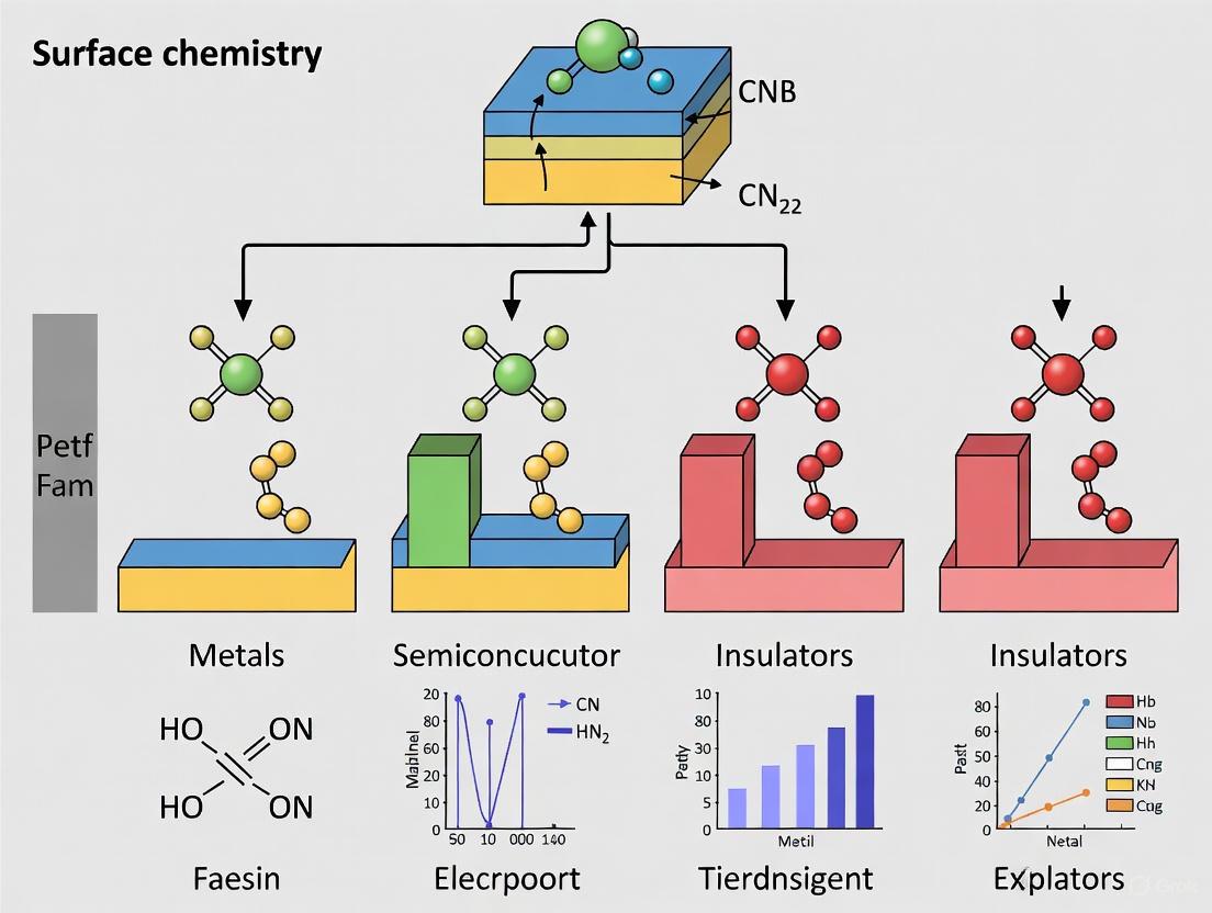
Surface Chemistry and Electronic Transport: Effects Across Material Classes for Next-Generation Devices
This article explores the critical role of surface chemistry in governing the electronic transport properties of diverse material classes, a fundamental consideration for advancing modern electronics and energy technologies.
Surface Chemistry and Electronic Transport: Effects Across Material Classes for Next-Generation Devices
Abstract
This article explores the critical role of surface chemistry in governing the electronic transport properties of diverse material classes, a fundamental consideration for advancing modern electronics and energy technologies. We examine foundational surface phenomena like electron accumulation and adsorption, detailing their material-specific impacts on semiconductors, layered 2D materials, metal oxides, and thermoelectrics. The scope extends to advanced characterization techniques, surface engineering strategies for performance optimization, and a comparative analysis of reliability and reproducibility across applications. Tailored for researchers and scientists, this review synthesizes key insights to guide the rational design of high-performance, stable electronic devices, from perovskite solar cells to sensors and catalytic systems.
Core Surface Phenomena and Their Fundamental Impact on Charge Transport
Adsorption, the adhesion of atoms, ions, or molecules from a gas, liquid, or dissolved solid to a surface, is a fundamental process in surface chemistry with profound implications across scientific and industrial domains. This process creates a film of the adsorbate on the surface of the adsorbent and is critically distinguished from absorption, where a substance diffuses into a liquid or solid to form a solution. The study of adsorption is pivotal for understanding and designing materials for applications ranging from environmental remediation and catalysis to energy harvesting and electronic devices. The mechanisms of adsorption are primarily categorized into two distinct types: physisorption (physical adsorption) and chemisorption (chemical adsorption), which differ fundamentally in their bonding nature, strength, and specificity.
The growing emphasis on nanotechnology and advanced materials has heightened the importance of surface chemistry, as the surface-to-volume ratio of materials increases dramatically at the nanoscale. Consequently, surface phenomena, including adsorption, begin to dominate the overall material behavior. As research by Iannicelli-Zubiani et al. highlights, characterizing the constituent particles' surface and interfaces is essential for understanding their influence on functional properties, significantly improving material design starting from the synthesis step [1]. This is particularly true in electronic transport research, where surface chemistry can drastically alter conductivity, as demonstrated in Bi₂Te₃ nanomaterials, where different synthetic routes led to vastly different electrical conductivity values due to variations in surface oxide content [1].
Comparative Analysis: Physisorption vs. Chemisorption
Understanding the distinctions between physisorption and chemisorption is crucial for selecting the appropriate process for specific applications. The table below summarizes the key differentiating characteristics.
Table 1: Fundamental Characteristics of Physisorption and Chemisorption
| Characteristic | Physisorption | Chemisorption |
|---|---|---|
| Bonding Type | Weak physical forces (van der Waals) | Strong chemical bonds (covalent, ionic) |
| Enthalpy Change (ΔH) | Low (≈ 20–40 kJ/mol) | High (≈ 200–400 kJ/mol) |
| Specificity | Non-specific | Highly specific |
| Reversibility | Readily reversible | Often irreversible or difficult to reverse |
| Temperature Dependence | Decreases with increasing temperature | May increase with temperature (activated process) |
| Surface Coverage | Multilayer formation possible | Typically limited to a monolayer |
| Electronic Impact | Minimal perturbation of electronic structure | Significant electron transfer/orbital rearrangement |
The mechanism of chemisorption often involves the formation of new hybrid orbitals between the adsorbate and atoms on the surface, with electron transfer occurring during the process [2]. For instance, in the adsorption of heavy metal ions like [Cu(OH)]+ onto kaolinite, density functional theory (DFT) calculations revealed an adsorption energy of -1.64 eV, indicating a strong chemical interaction [2]. In contrast, physisorption lacks such significant electron sharing or transfer and is dominated by nonspecific, weaker interactions. The choice between these mechanisms directly impacts material performance; for example, in thermoelectric materials, surface oxide layers formed via chemisorption can create a resistive barrier that drastically lowers electrical conductivity [1].
Adsorption Performance Across Material Classes
The efficacy of adsorption is highly dependent on the adsorbent material. The following table compares the performance of various materials in adsorbing different heavy metal ions, a key application in environmental remediation.
Table 2: Comparison of Adsorption Performance for Heavy Metal Ions on Different Adsorbents
| Adsorbent Material | Target Adsorbate | Max Adsorption Capacity (mg/g) | Optimal pH | Primary Adsorption Mechanism | Reference |
|---|---|---|---|---|---|
| Kaolinite Clay | Zn(II) | 15.52 | 5.0 | Surface complexation, Ion exchange | [2] |
| Kaolinite Clay | Pb(II) | 61.52 | 5.0 | Surface complexation, Ion exchange | [2] |
| Kaolinite Clay | Cu(II) | 44.66 | 5.0 | Surface complexation, Ion exchange | [2] |
| Lignin-derived Biochar (500°C) | Cd(II) | 635.44 | ~5-7 | Surface complexation, Ionic exchange, Co-precipitation | [3] |
| Amino-functionalized Fe₃O₄ | Cr(VI) | 232.51 | 3.0 | Electrostatic attraction, Chemical binding | [4] |
| EDA-MPMs | Cr(VI) | 236.90 | 2.0 | Electrostatic attraction, Chemical binding | [4] |
The data reveals significant variations in performance based on both the adsorbent and adsorbate. For example, kaolinite shows a strong affinity for Pb(II) and Cu(II) over Zn(II), which DFT simulations attribute to differences in adsorption energy ([Cu(OH)]+ at -1.64 eV vs. [Zn(OH)]+ at -0.49 eV) [2]. Functionalization with specific groups, such as thiols or amines, can dramatically enhance performance by providing strong binding sites. A review of mercury removal technologies noted that both adsorption and membranes can be enhanced by the addition of functional groups like thiols, where sulfur serves as a strong binding site for mercury ions [5]. Furthermore, synthesis conditions, such as the pyrolysis temperature for biochar, directly influence the material's properties and its dominant adsorption mechanisms [3].
Experimental Protocols for Adsorption Studies
Batch Adsorption Experimentation
A standard methodology for evaluating adsorption performance in aqueous systems involves batch experiments [2]. The following workflow outlines the key steps.
Diagram 1: Batch Adsorption Workflow
Step-by-Step Protocol:
- Stock Solution Preparation: Prepare a primary stock solution of the target adsorbate (e.g., heavy metal salt like
Pb(NO₃)₂) in deionized water at a high concentration (e.g., 1000 mg/L). Subsequent working solutions are prepared by dilution [2]. - pH Adjustment: The pH of the solution is adjusted using dilute acids (e.g.,
HNO₃) or bases (e.g.,NaOH) to the desired value. This is a critical step as pH profoundly affects the surface charge of the adsorbent and the chemical speciation of the adsorbate [2] [4]. - Adsorbent Addition: A precisely weighed quantity of the adsorbent is added to a known volume of the adsorbate solution in a sealed container like a conical flask [2].
- Agitation and Equilibration: The mixture is agitated at a constant speed and temperature in an orbital shaker for a predetermined time to reach equilibrium [2].
- Separation: After agitation, the solid adsorbent is separated from the liquid phase via filtration or centrifugation. Using a 0.45 μm pore size filter is a common practice [2].
- Analysis: The concentration of the residual adsorbate in the supernatant is quantified using analytical techniques such as Inductively Coupled Plasma Optical Emission Spectrometry (ICP-OES) [2].
- Calculation: The adsorption capacity at equilibrium,
qₑ(mg/g), is calculated using the mass balance equation:qₑ = (C₀ - Cₑ)V / m, whereC₀andCₑare the initial and equilibrium concentrations (mg/L),Vis the solution volume (L), andmis the mass of the adsorbent (g) [2].
Material Characterization and Computational Methods
A comprehensive adsorption study integrates advanced characterization and modeling.
- Material Characterization: Key techniques include:
- Scanning Electron Microscopy with Energy-Dispersive X-ray Spectroscopy (SEM-EDS): For analyzing surface morphology and elemental composition before and after adsorption [2].
- X-ray Diffraction (XRD): To determine crystal structure and any changes in layer spacing post-adsorption [2].
- Fourier-Transform Infrared (FT-IR) Spectroscopy: To identify functional groups on the adsorbent surface and observe shifts or changes after adsorption, indicating binding [2].
- X-ray Photoelectron Spectroscopy (XPS): Used to determine surface chemistry and elemental oxidation states, which can reveal the presence of surface oxides or other chemical states that impact performance [1].
- Computational Modeling: Density Functional Theory (DFT) calculations are employed to understand adsorption mechanisms at the atomic level. This involves calculating parameters like adsorption energy, electronic density of states, and charge transfer. For example, simulations can show how metal ions like
[Cu(OH)]+adsorb on the (001) surface of kaolinite, providing adsorption energy values and revealing the formation of new hybrid orbitals [2]. High-throughput databases of electronic transport properties, calculated using codes like BoltzTraP based on DFT, are also valuable resources for predicting material behavior [6].
The Scientist's Toolkit: Essential Research Reagents and Materials
Table 3: Key Reagents and Materials for Adsorption Research
| Item / Reagent | Function / Application | Representative Example |
|---|---|---|
| Kaolinite | A natural, low-cost clay mineral adsorbent with aluminosilicate layers. | Adsorption of Zn(II), Pb(II), and Cu(II) ions from aqueous solutions [2]. |
| Functionalized Biochar | Porous carbon material from pyrolyzed biomass; high adsorption capacity. | Lignin-derived biochar for Cd(II) removal; functionality enhances capacity [3]. |
| Magnetic Nanoparticles (e.g., Fe₃O₄) | Nano-adsorbents functionalized for targeted adsorption; easily separated via magnet. | Amino-functionalized Fe₃O₄ for Cr(VI) removal [4]. |
| Heavy Metal Salts (e.g., Pb(NO₃)₂) | Source of adsorbate ions (e.g., Pb²⁺) in batch adsorption experiments. |
Used to prepare stock solutions for testing adsorbent efficacy [2]. |
| ICP-OES | Analytical instrument for precise quantification of metal ion concentrations in solution. | Measuring residual metal concentration after adsorption to calculate qₑ [2]. |
Adsorption Mechanisms and Impact on Electronic Transport
The interplay between adsorption mechanisms and electronic properties is a critical frontier in materials science. Surface chemistry can profoundly influence electronic transport, a key consideration for devices like thermoelectrics, sensors, and transistors.
Surface Chemistry and Charge Transfer
Chemisorption often involves significant charge transfer between the adsorbate and the adsorbent surface. As demonstrated in kaolinite-heavy metal systems, new hybrid orbitals are formed between the metal ions and oxygen atoms on the surface, with clear electron transfer occurring during the adsorption process [2]. This charge transfer can dope the material, altering its carrier concentration and Fermi level. For instance, pristine surfaces of layered materials like MoS₂ exhibit a major n-doping source, with the surface electron concentration being nearly four orders of magnitude higher than that of its inner bulk [7]. This Surface Electron Accumulation (SEA) leads to two-dimensional electronic transport and substantial thickness-dependent conductivity, contradicting the expectation for a uniform conductor [7].
The Role of Resistive Surface Layers
The formation of surface layers through chemisorption can create resistive barriers that impede electronic transport. A comparative study of Bi₂Te₃ synthesized via hydrothermal and thermolysis routes found that the hydrothermal sample had a higher metal oxide content on its surface. This oxide layer acted as a resistive barrier, lowering the electrical conductivity by a factor of eight compared to the thermolysis sample [1]. This phenomenon was further confirmed by Arrhenius plots, which showed a higher activation energy for conduction in the sample with the higher surface oxide content [1]. The logical relationship between surface chemistry, adsorption, and electronic transport is summarized below.
Diagram 2: Surface Chemistry Impact on Electronics
Implications for Material Design
Understanding these mechanisms allows for intelligent material design. To mitigate unwanted surface doping effects, strategies like in-situ cleaving can be employed to create fresh, nearly intrinsic surfaces without electron accumulation [7]. Alternatively, synthesis routes can be selected to minimize the formation of resistive surface layers; for thermoelectric materials, the thermolysis route for Bi₂Te₃ is recommended over the hydrothermal route due to its superior electronic transport properties [1]. Furthermore, computational screening using DFT and Boltzmann transport theory, as implemented in high-throughput databases, enables the prediction and selection of materials with desired transport properties before synthesis [6].
Surface Electron Accumulation (SEA) is an intriguing quantum phenomenon in semiconductors where the electron concentration at the material's surface becomes significantly higher than in its inner bulk region. This effect is particularly pronounced in low-dimensional and layered materials due to their inherently high surface-to-volume ratio, making surface properties dominant in determining their overall electronic behavior. Van der Waals crystals, such as transition metal dichalcogenides (TMDs), were traditionally expected to possess inert surfaces because of the absence of dangling bonds. However, recent research has conclusively demonstrated that the pristine surface of these materials can be a major n-doping source, with the surface electron concentration in molybdenum disulfide (MoS₂) found to be nearly four orders of magnitude higher than that of its inner bulk [7] [8]. This discovery has fundamentally altered our understanding of electronic transport in layered materials and has profound implications for designing novel electronic and catalytic devices.
The emergence of SEA challenges conventional semiconductor physics, where surfaces typically exhibit electron depletion rather than accumulation. This anomalous behavior was initially identified in a limited class of bulk semiconductors, including InAs, InN, CdO, and In₂O₃, but has now been observed in several two-dimensional TMDs, revealing a common characteristic across different material systems [9]. Understanding SEA is crucial for practically controlling the intrinsic properties of layered semiconductors and fabricating both p-type and n-type devices from the same material system. The phenomenon is not merely a surface curiosity but a dominant factor that governs electronic transport, catalytic activity, and optical properties in nanostructured forms of these materials, necessitating a comprehensive investigation into its origins, manifestations, and applications.
Comparative Analysis of SEA Across Material Systems
Manifestations in Transition Metal Dichalcogenides
The SEA phenomenon exhibits both universal characteristics and material-specific variations across different TMDs. Experimental investigations have revealed that SEA is a prevalent feature in synthesized MoS₂ and MoSe₂ crystals, though the specific mechanisms and magnitudes differ. In MoS₂, the surface electron concentration reaches remarkably high values, creating a substantial conductivity gradient between the surface and bulk regions. This results in two-dimensional electronic transport behavior rather than conventional three-dimensional conduction, fundamentally altering the current transport mechanisms in these materials [7]. The thickness-dependent conductivity studies show an inverse power law relationship where conductivity (σ) decreases with increasing thickness (t), following σ ∝ t^(-β) with β ≈ 1.1 ± 0.16, unequivocally demonstrating the surface-dominated nature of electronic transport [7].
In MoSe₂, research has uncovered an anomalously high electron concentration at the surface reaching up to 10¹⁹ cm⁻³, several orders of magnitude higher than the bulk concentration of 3.6 × 10¹² cm⁻³ [9]. This pronounced accumulation effect has been directly linked to selenium vacancies formed through spontaneous deselenization at room temperature, which act as donor-like surface states. The spontaneous formation of these vacancies occurs not only during crystal growth but also through mechanical exfoliation processes, indicating the inherent instability of the pristine surface and its tendency toward SEA formation. Unlike conventional semiconductors where surface states typically pin the Fermi level and lead to depletion, these vacancy-induced states in TMDs create a robust accumulation layer that significantly enhances surface conductivity.
Table 1: Quantitative Comparison of SEA Properties in Different Materials
| Material | Surface Electron Concentration | Bulk Electron Concentration | Primary Origin of SEA | Key Characterization Techniques |
|---|---|---|---|---|
| MoS₂ | Nearly 10⁴ × higher than bulk | ~10¹⁰ cm⁻³ | Surface n-doping source, likely sulfur vacancies | STM/STS, ARPES, thickness-dependent conductivity [7] |
| MoSe₂ | Up to 10¹⁹ cm⁻³ | 3.6 × 10¹² cm⁻³ | Selenium vacancies from deselenization | STM/STS, Hall effect, plasma treatment [9] |
| BaSnO₃ (LBSO) | 2D metallic surface state | 3D bulk conduction band | Surface termination, polar interfaces | ARPES, ab initio calculations [10] |
Comparison with Transparent Conducting Oxides
Beyond TMDs, the SEA phenomenon manifests in transparent conducting oxides (TCOs) such as La-doped BaSnO₃ (LBSO), though through different physical mechanisms. ARPES studies of LBSO films have revealed the existence of a two-dimensional metallic state at the SnO₂-terminated surface, characterized by a distinct carrier density and significantly lower effective mass (approximately 0.12mₑ) compared to the bulk conduction band [10]. This 2D state exhibits cylindrical Fermi surfaces rather than the spherical Fermi surface expected for bulk states, confirming its confined nature at the surface. The emergence of this surface state in perovskite stannates underscores the role of polar interfaces and surface termination in driving electron accumulation, contrasting with the vacancy-driven mechanisms in TMDs.
The comparative analysis between these material classes reveals that while the macroscopic manifestation of SEA is similar—enhanced surface conductivity—the underlying physical origins differ substantially. TMDs primarily exhibit defect-mediated accumulation through chalcogen vacancies, whereas TCOs display termination-dependent electronic reconstruction at polar surfaces. This distinction has profound implications for device applications: vacancy-driven SEA can be controlled through environmental conditions and surface passivation, while termination-dependent SEA requires atomic-level surface engineering. Despite these different origins, both systems demonstrate the universal tendency of low-dimensional and layered materials to develop anomalous surface electronic states that dominate their transport properties.
Experimental Methodologies for SEA Investigation
Material Synthesis and Characterization Protocols
The investigation of SEA phenomena begins with the synthesis of high-quality single crystals employing standardized protocols. For TMDs such as MoS₂ and MoSe₂, the chemical vapor transport (CVT) method has proven particularly effective. In this approach, the source and crystallization ends are maintained at precisely controlled temperatures (1050°C and 960°C, respectively, for MoSe₂) using bromine as a transport agent [9]. This method yields single-crystals with excellent crystalline quality, as evidenced by sharp X-ray diffraction peaks corresponding to (00l) planes and narrow Raman peaks, confirming single-out-of-plane orientation and high crystallinity [7] [9].
Structural characterization forms the foundation for correlating morphological properties with electronic behavior. X-ray diffraction (XRD) measurements confirm phase purity and crystallographic orientation, while Raman spectroscopy provides information about phonon modes and layer-dependent characteristics. For MoS₂, the characteristic E₁₂g and A₁g modes at 383.1 and 408.2 cm⁻¹, respectively, with narrow peak widths of 3.1 and 3.7 cm⁻¹, indicate excellent crystalline quality [7]. Atomic force microscopy (AFM) is indispensable for determining the precise thickness of exfoliated nanoflakes, which is crucial for correlating thickness with electronic transport properties. These structural characterization techniques collectively ensure that the investigated materials possess the necessary quality for reliable SEA measurement and analysis.
Direct Surface-Sensitive Measurement Techniques
The direct experimental confirmation of SEA requires surface-sensitive probes that can distinguish between surface and bulk electronic properties. Scanning tunneling microscopy and spectroscopy (STM/STS) have been instrumental in this regard, enabling direct measurement of local density of states (LDOS) with atomic-scale resolution. STS measurements on MoSe₂ surfaces have revealed a pronounced increase in LDOS near the conduction band minimum at the surface compared to the bulk, providing direct evidence of electron accumulation [9]. This technique allows for the correlation of electronic properties with specific surface features, including vacancies and defects.
Angle-resolved photoemission spectroscopy (ARPES) provides complementary information by measuring the band dispersion and Fermi surface topology. ARPES studies on LBSO films have identified 2D metallic surface states with cylindrical Fermi surfaces, distinctly different from the 3D bulk states [10]. The k₂ independence of these states confirms their 2D character and surface confinement. For materials exhibiting SEA, ARPES shows the Fermi level positioned well above the conduction band minimum at the surface, in contrast to the bulk where it lies closer to the band edge. These surface-sensitive techniques collectively provide unambiguous evidence of SEA and enable quantitative analysis of its energy distribution and momentum space characteristics.
Table 2: Experimental Techniques for SEA Characterization
| Technique | Primary Function | Key Parameters Measured | Material Systems Applied |
|---|---|---|---|
| STM/STS | Surface electronic structure mapping | Local density of states, defect states | MoS₂, MoSe₂ [7] [9] |
| ARPES | Band structure determination | Band dispersion, Fermi surface topology | BaSnO₃, MoS₂ [7] [10] |
| Thickness-dependent conductivity | Transport dimensionality | Conductivity vs. thickness relationship | MoS₂, MoSe₂ [7] [9] |
| Transfer length method (TLM) | Current transport mode analysis | 2D vs. 3D transport behavior | MoS₂ [7] |
| Temperature-dependent conductivity | Carrier activation energy | Thermal activation energy (Eₐ) | MoS₂ [7] |
Electronic Transport Measurement Approaches
Electronic transport measurements provide indirect but crucial evidence for SEA through thickness-dependent and temperature-dependent conductivity studies. The transfer length method (TLM) has demonstrated that current transport in MoS₂ follows a two-dimensional behavior rather than the conventional three-dimensional mode, indicating surface-dominated conduction [7]. This represents a significant departure from bulk transport models and highlights the critical importance of surface effects in low-dimensional materials.
Temperature-dependent conductivity measurements reveal distinct thermal activation energies for nanoflakes versus bulk crystals. For MoS₂, nanoflakes exhibit a much smaller activation energy (6 meV) compared to bulk crystals (68 meV), indicating different origins of majority carriers despite being exfoliated from the same bulk crystal [7]. This substantial difference further corroborates the surface-dominated transport in thin flakes. Additionally, Hall effect measurements provide quantitative information about carrier concentration and mobility, clearly showing enhanced carrier density in surface-rich samples compared to bulk specimens. These transport measurements, when combined with direct surface-sensitive techniques, form a comprehensive experimental framework for identifying and characterizing SEA in diverse material systems.
The Scientist's Toolkit: Essential Research Reagents and Materials
The experimental investigation of SEA requires specialized materials and analytical tools that enable precise synthesis, processing, and characterization of low-dimensional materials. The following comprehensive toolkit outlines the essential components for research in this field:
Table 3: Essential Research Toolkit for SEA Investigations
| Category | Specific Items | Function & Application | Representative Examples |
|---|---|---|---|
| Synthesis Materials | High-purity Mo, S, Se powders; Br₂ transport agent | Single crystal growth via CVT method | MoS₂, MoSe₂ bulk crystals [9] |
| Characterization Tools | XRD spectrometer; Raman microscope; AFM | Structural characterization and thickness measurement | Phase identification, layer number determination [7] [9] |
| Surface Analysis Instruments | STM/STS system; ARPES facility | Direct measurement of surface electronic structure | LDOS mapping, band dispersion [7] [9] [10] |
| Electronic Measurement Systems | Probe station; Hall effect system; TLM structures | Electrical transport characterization | Conductivity, carrier concentration, mobility [7] |
| Surface Modification Tools | Plasma treatment systems; Environmental chambers | Controlled surface defect engineering | Nitrogen plasma treatment of MoSe₂ [9] |
The research toolkit highlights the multidisciplinary nature of SEA investigations, spanning materials synthesis, physical characterization, and device fabrication. The CVT growth technique using bromine transport agents enables the production of high-quality single crystals with minimal intrinsic defects, providing the foundational material for SEA studies [9]. Surface-sensitive tools like STM/STS and ARPES are indispensable for directly probing the electronic structure anomalies associated with SEA, while electronic transport measurements provide complementary evidence through thickness-dependent and temperature-dependent studies [7] [10]. The inclusion of surface modification tools such as plasma treatment systems enables controlled studies of defect engineering on SEA properties, particularly relevant for optimizing materials for specific applications like electrocatalysis [9].
Impact and Applications of SEA in Functional Devices
Enhanced Electrocatalytic Performance
The presence of SEA has demonstrated significant benefits in electrocatalytic applications, particularly for the hydrogen evolution reaction (HER). In MoSe₂, the conjugate formation of surface defects and conductive electrons associated with SEA substantially enhances HER activity on otherwise inert basal planes [9]. The optimized HER efficiency achieved through nitrogen plasma treatment of 2H-MoSe₂ demonstrates overpotentials as low as 0.17 V and Tafel slopes of 60 mV/dec, outperforming many nanostructured and hybrid counterparts [9]. This remarkable enhancement stems from the dual role of chalcogen vacancies, which not only generate the donor states responsible for SEA but also create active sites for electrochemical catalysis.
The connection between SEA and catalytic activity represents a paradigm shift in catalyst design principles. Rather than relying solely on edge sites or phase engineering, the deliberate creation and control of SEA through defect engineering offers a powerful strategy for activating the basal plane of layered materials. The high surface electron concentration facilitates charge transfer processes crucial for electrochemical reactions, while the vacancy sites lower the activation energy for reaction intermediates. This synergistic effect between electronic structure modification and catalytic activity optimization highlights the practical importance of understanding and controlling SEA phenomena for energy conversion technologies.
Implications for Electronic and Optoelectronic Devices
SEA has profound implications for electronic and optoelectronic devices based on layered materials. The anomalously high electron concentration at surfaces significantly impacts contact resistance, carrier injection, and overall device performance. In field-effect transistors based on MoS₂, the residual carrier concentration at zero gate voltage is much higher in monolayers (~5.6 × 10¹² cm⁻²) than in bulk counterparts (~1.6 × 10¹⁰ cm⁻²), posing challenges for achieving complete current saturation but enabling high on/off ratios in depletion-mode operation [7]. This intrinsic n-doping effect influences threshold voltage control and limits the fabrication of p-type devices, necessitating specialized approaches for carrier type control.
For transparent conducting oxides like BaSnO₃, the 2D metallic surface states associated with SEA offer opportunities for engineering highly conductive heterostructures without compromising optical transparency [10]. The significantly lower effective mass of surface electrons compared to bulk carriers (0.12mₑ vs. 0.17mₑ) enhances mobility and conductivity in ultrathin films, making these materials promising for transparent electrodes in displays, photovoltaics, and optoelectronic devices. The ability to control and manipulate SEA through surface treatments, environmental conditions, and thickness engineering provides an additional degree of freedom for optimizing device performance across various applications.
Surface Electron Accumulation has emerged as a predominant effect governing the electronic properties of low-dimensional and layered materials. This phenomenon, characterized by electron concentrations at surfaces that can be several orders of magnitude higher than in the bulk, directly impacts material behavior across multiple TMDs and transparent conducting oxides. The experimental evidence from surface-sensitive probes and transport measurements consistently reveals the fundamental role of surfaces in determining the electronic characteristics of these materials, necessitating a reevaluation of traditional bulk-dominated transport models.
The implications of SEA extend beyond fundamental scientific interest to practical applications in catalysis, electronics, and energy technologies. The deliberate engineering of SEA through defect control and surface treatments offers a powerful approach for optimizing material performance, as demonstrated by the enhanced HER activity in MoSe₂ basal planes. As research in low-dimensional materials continues to advance, a comprehensive understanding of SEA will be indispensable for harnessing the unique properties of these materials for next-generation technologies. Future investigations focusing on the dynamic control of SEA through external stimuli and the development of strategies for achieving p-type accumulation layers will further expand the technological landscape for these remarkable materials.
In the development of next-generation electronic and energy conversion devices, the performance of functional materials is often dominated not by their bulk properties, but by the behavior of their surfaces and interfaces. This review provides a comparative analysis of three distinct material classes—inorganic electron transport layers (ETLs) for photovoltaics, two-dimensional transition metal dichalcogenides (2D TMDs) for electronics, and advanced materials for thermoelectric applications—through the unifying lens of surface and interface effects on electronic transport. Each of these material systems exhibits unique surface-dominated phenomena that critically influence charge carrier extraction, transport efficiency, and overall device performance. By examining recent advances in surface engineering, interface modification, and characterization techniques across these diverse material systems, this review aims to provide researchers with a comprehensive understanding of how surface chemistry can be harnessed to optimize electronic transport properties for specific technological applications.
Inorganic Electron Transport Layers (ETLs) in Perovskite Solar Cells
Performance Comparison of Major Inorganic ETL Materials
Inorganic electron transport layers play a vital role in perovskite solar cells (PSCs) by facilitating charge extraction, transport, and recombination suppression. The search for alternatives to organic ETLs has intensified due to limitations in the latter's thermal, optical, and moisture stability [11]. Table 1 summarizes the key performance characteristics of the most widely studied inorganic ETL materials.
Table 1: Performance Comparison of Major Inorganic ETL Materials for Perovskite Solar Cells
| Material | Electron Mobility (cm²/V·s) | Band Gap (eV) | Processing Temperature | Key Advantages | Limitations | Best Reported PCE (%) |
|---|---|---|---|---|---|---|
| TiO₂ | Low (~1) | 3.2 | High (>450°C) | Historical benchmark, high thermal stability | Photocatalytic instability, low electron mobility, high defect density | ~25 [11] |
| SnO₂ | High (>200) | 3.5-4.0 | Low (<200°C) | Superior electron mobility, excellent optical transparency, low-temperature processability | Requires interface engineering | 26.61 [11] |
| ZnO | Medium (~30) | 3.3 | Low (<200°C) | High conductivity, facile synthesis | Chemical instability concerns, reacts with perovskites | ~20 [11] |
Surface Engineering Strategies for Enhanced ETL Performance
The performance disparities observed in Table 1 highlight the critical importance of surface and interface properties. While TiO₂ has historically been the benchmark ETL, challenges such as high-temperature processing requirements and photocatalytic instability under light exposure have driven research toward alternative materials [11]. SnO₂ has emerged as a particularly promising candidate due to its superior electron mobility, low-temperature processability, and excellent optical transparency.
Surface modification techniques have proven essential for optimizing ETL performance. For SnO₂-based ETLs, interface engineering through doping strategies and surface passivation has been crucial for minimizing interfacial recombination centers and improving charge extraction efficiency [11]. These approaches directly address surface defect states that would otherwise trap charge carriers and reduce device performance. Similarly, ZnO ETLs benefit from surface stabilization treatments that mitigate their tendency to react with perovskite layers, though stability concerns remain a significant challenge [11].
Table 2: Experimental Protocols for ETL Characterization and Performance Evaluation
| Experimental Technique | Key Measured Parameters | Experimental Details | Information Gained |
|---|---|---|---|
| Current-Voltage (I-V) Characterization | Power conversion efficiency (PCE), open-circuit voltage (VOC), short-circuit current density (JSC), fill factor (FF) | Standard AM 1.5G illumination conditions, scan rate of 10-100 mV/s, active area typically 0.05-0.2 cm² | Overall device performance, charge extraction efficiency, series/shunt resistance effects |
| Electrochemical Impedance Spectroscopy (EIS) | Charge transfer resistance, recombination resistance, chemical capacitance | Frequency range: 0.1 Hz to 1 MHz, AC amplitude: 10-20 mV, under illumination and dark conditions | Interface quality, charge recombination kinetics, defect state distribution |
| Ultraviolet Photoelectron Spectroscopy (UPS) | Work function, valence band maximum, ionization energy | He I radiation (21.22 eV), sample bias typically -5 to -10 V, energy resolution <0.1 eV | Energy level alignment at ETL/perovskite interface, band bending effects |
| Space-Charge-Limited Current (SCLC) | Trap density, charge carrier mobility | Dark I-V measurements on electron-only devices (e.g., FTO/ETL/PCBM/Ag), voltage range 0-6 V | Defect density in ETL materials, charge transport properties |
Diagram 1: Electronic transport processes and recombination pathways at the ETL/perovskite interface. Surface states significantly impact device performance by promoting recombination.
Two-Dimensional Transition Metal Dichalcogenides (TMDs)
Electronic Transport Properties and Surface Effects
Two-dimensional transition metal dichalcogenides (TMDs) such as MoS₂, MoSe₂, WS₂, and WSe₂ represent a promising class of semiconducting materials for next-generation electronic devices. Their electronic transport properties are exceptionally sensitive to surface conditions and interface quality due to their extremely high surface-to-volume ratio [7]. Table 3 compares the key properties of prominent 2D TMD materials relevant to electronic transport.
Table 3: Electronic and Mechanical Properties of 2D TMD Materials
| Material | Band Gap (eV) | Carrier Mobility (cm²/V·s) | Young's Modulus (GPa) | Fracture Strain (%) | Unique Features | Primary Applications |
|---|---|---|---|---|---|---|
| MoS₂ | ~1.3 (indirect bulk), ~1.9 (direct monolayer) | 10-200 | 170-330 | 6-11 | Most extensively studied, high on/off ratio | FETs, sensors, photodetectors |
| WS₂ | ~2.0 (direct monolayer) | 10-150 | 150-250 | 6-10 | Strong spin-orbit coupling, valley polarization | Optoelectronics, valleytronics |
| WSe₂ | ~1.7 (direct monolayer) | 50-200 | 150-250 | 6-10 | Ambipolar transport, high mobility | Complementary electronics, LEDs |
| MoSe₂ | ~1.6 (direct monolayer) | 50-150 | 120-200 | 6-10 | Tunable band structure | Photovoltaics, flexible electronics |
A remarkable surface phenomenon in 2D TMDs is surface electron accumulation (SEA). Studies on high-quality synthesized MoS₂ have revealed that the surface electron concentration can be nearly four orders of magnitude higher than that of its inner bulk [7]. This substantial thickness-dependent conductivity results in current transport following a two-dimensional behavior rather than the conventional three-dimensional mode [7]. The surface of MoS₂ acts as a major n-doping source, explaining the unusually high electron concentration in unintentionally doped layer semiconductors and the difficulty in fabricating intrinsic and p-type MoS₂ nanostructures [7].
Contact Engineering and Interface Optimization
The performance of 2D TMD-based devices is critically limited by contact resistance at the metal-semiconductor interface. The Fermi level pinning effect introduces uncontrollable Schottky barriers at metal-2D-TMD contacts, challenging prediction through the conventional Schottky-Mott rule [12]. These barriers lead to elevated contact resistance and limited current-delivery capability, impeding the enhancement of 2D-TMD transistor properties [12].
Advanced contact engineering strategies have emerged to address these challenges:
- Van der Waals contacts: This approach involves transferring pre-fabricated metal electrodes onto 2D TMDs, minimizing direct chemical bonding and disorder-induced gap states at the interface [12].
- Interface interaction and hybridization: Modifying the interface with ultrathin oxides or self-assembled monolayers can reduce the metal-induced gap states and depin the Fermi level [12].
- Charge-transfer doping: Using high-work function oxides like MoO₃ or molecular dopants can effectively tune the carrier concentration and reduce the Schottky barrier height [12].
- Phase engineering: Creating metallic phases (1T or 1T') in specific contact regions enables ohmic contact formation with lower resistance [12].
Diagram 2: Contact engineering strategies for overcoming Fermi level pinning (FLP) and high contact resistance in 2D TMD devices.
Experimental Protocols for 2D TMD Characterization
Table 4: Experimental Methods for Analyzing Surface and Transport Properties in 2D TMDs
| Technique | Measurement Principles | Key Parameters | Surface/Interface Information |
|---|---|---|---|
| Transfer Length Method (TLM) | Multiple electrode measurements with varying channel lengths | Contact resistance, transfer length, sheet resistance | 2D versus 3D current transport behavior, interface quality [7] |
| Scanning Tunneling Microscopy/Spectroscopy (STM/STS) | Quantum tunneling current between sharp tip and sample | Surface topography, local density of states, defect states | Direct evidence of surface electron accumulation, atomic-scale defects [7] |
| Angle-Resolved Photoemission Spectroscopy (ARPES) | Photoelectron emission momentum mapping | Band structure, band dispersion, Fermi surface | Electronic band structure, surface states, doping effects [7] |
| Raman Spectroscopy | Inelastic light scattering by phonons | Layer thickness, strain, doping, defect density | Crystal quality, layer number, strain effects, doping levels [7] |
Thermoelectric Materials
Performance Metrics and Surface Chemistry Considerations
Thermoelectric materials convert temperature gradients directly into electrical voltage and vice versa, offering promising applications in waste heat recovery and solid-state cooling. The performance of thermoelectric materials is quantified by the dimensionless figure of merit, zT = (S²σ/κ)T, where S is the Seebeck coefficient, σ is electrical conductivity, κ is thermal conductivity, and T is absolute temperature. Table 5 compares the performance characteristics of selected advanced thermoelectric materials.
Table 5: Performance Comparison of Advanced Thermoelectric Materials
| Material System | Optimal Temperature Range | Peak zT Value | Key Advantages | Surface/Interface Challenges |
|---|---|---|---|---|
| BaSe | 500-800 K | 1.51 (unstrained, 800K) [13] | High anharmonicity, low lattice thermal conductivity | Surface oxidation affecting carrier transport |
| Bi₂Te₃ | 300-400 K | ~1.0 (bulk) | Industry standard near room temperature | Surface oxide layers increase contact resistance [1] |
| Mg₃(Sb,Bi)₂ | 300-600 K | ~1.8 (reported) | Earth-abundant elements, high performance | Interface stability during processing |
| Hydrothermal Bi₂Te₃ | 300-500 K | Lower than thermolysis | Aqueous synthesis, greener process | Higher oxide content creates resistive barriers [1] |
| Thermolysis Bi₂Te₃ | 300-500 K | 8× higher conductivity than hydrothermal [1] | Better surface chemistry control, higher conductivity | Requires organic solvents, higher cost |
Surface chemistry plays a decisive role in thermoelectric performance, particularly in nanostructured materials where the surface-to-volume ratio is high. Comparative studies of Bi₂Te₃ synthesized through hydrothermal and thermolysis routes have revealed significant differences in transport properties connected to their surface chemistry [1]. XPS analysis has shown that hydrothermally synthesized Bi₂Te₃ contains a higher metal oxide content at the surface, contributing to the formation of a resistive layer that lowers electrical conductivity [1]. This surface oxide layer creates a potential barrier for charge carriers, effectively reducing the electrical conductivity by about eight times compared to thermolysis-synthesized Bi₂Te₃ with cleaner surfaces [1].
Strain Engineering and Advanced Design Approaches
Strain engineering has emerged as a powerful strategy for optimizing the thermoelectric performance of material systems. Applied compression and tensile strain can significantly alter electronic band structures and phonon dispersion relations, enabling independent optimization of electrical and thermal transport properties. Studies on alkaline earth metal selenide (AEMSe) compounds under various strain conditions (-5%, 0%, and +5%) have demonstrated that strain can effectively tune band degeneracy and carrier effective mass, leading to enhancements in the Seebeck coefficient and electrical conductivity [13].
Advanced computational and inverse design approaches are accelerating the development of high-performance thermoelectric materials. Recent work has introduced generative models combining diversity loss functions and residual network (ResNet) architecture to predict novel thermoelectric compositions with high zT values [14]. This approach has successfully identified 100 doped materials with zT values exceeding 1.0, with experimental validation of representative materials such as Mg₃.₁Sb₀.₅Bi₁.₄₉₇Te₀.₀₀₃ from the Mg₃(Sb, Bi)₂ family [14].
Table 6: Experimental Methods for Thermoelectric Material Characterization
| Characterization Technique | Measurement Parameters | Experimental Configuration | Surface-Related Information |
|---|---|---|---|
| Seebeck Coefficient & Electrical Conductivity | S, σ simultaneously | Two-probe or four-probe configuration, temperature gradient 1-10K, vacuum environment | Surface oxide effects on carrier transport, contact resistance |
| Thermal Conductivity | κ = κₑ + κₗ | Laser flash analysis (LFA) for thermal diffusivity, specific heat measurement | Surface scattering of phonons, interface contributions |
| X-ray Photoelectron Spectroscopy (XPS) | Surface elemental composition, oxidation states | Monochromatic Al Kα radiation, depth profiling with Ar⁺ sputtering | Surface chemistry, oxide layer thickness and composition [1] |
| Electrophoretic Deposition (EPD) | Film quality, interfacial contacts | Colloidal suspension in organic solvent, DC field 10-100 V/cm | Platform for studying surface chemistry effects on transport [1] |
Diagram 3: Competing surface effects in thermoelectric materials. Surface oxides can both reduce electrical conductivity (σ) through carrier scattering and reduce thermal conductivity (κ) through phonon scattering, creating complex optimization challenges.
The Scientist's Toolkit: Essential Research Reagents and Materials
Table 7: Key Research Reagents and Materials for Surface and Electronic Transport Studies
| Reagent/Material | Function/Application | Specific Examples | Relevance to Surface/Interface Effects |
|---|---|---|---|
| Diethylzinc (DEZ) | Precursor for ZnO ETL deposition via vapor-phase infiltration | Formation of ZnO electron transport layers [15] | Enables low-temperature processing with controlled interface properties |
| Trimethylaluminum (TMA) | Molecular precursor for Al₂O₃ interfacial layers | Surface passivation, interface modification [15] | Reduces interface defects and improves charge extraction |
| Titanium Isopropoxide | TiO₂ precursor for sol-gel and infiltration processes | TiO₂ ETL formation, hybrid organic-inorganic interfaces [15] | Controls crystallization and surface chemistry of oxide layers |
| PCBM ([60]PCBM) | Organic electron acceptor and transport material | ETL in perovskite solar cells, interface modifier [11] | Passivates interface defects, improves energy level alignment |
| Transition Metal Dichalcogenide Precursors | CVD growth of 2D TMD layers | MoO₃, WO₃, S, Se for TMD synthesis [16] | Determines crystal quality, defect density, and ultimate electronic properties |
| High-Work-Function Metal Oxides | Charge-transfer dopants for 2D TMDs | MoO₃, V₂O₅ for p-type doping [12] | Modulates Fermi level position, reduces Schottky barrier height |
| Bismuth Telluride Precursors | Thermoelectric material synthesis | BiCl₃, Te powder for hydrothermal/thermolysis routes [1] | Synthetic route determines surface chemistry and oxide content |
This comparative analysis of inorganic ETLs, 2D TMDs, and thermoelectric materials reveals the universal importance of surface and interface chemistry in governing electronic transport properties across diverse material classes. While each material system faces unique challenges—interface recombination in ETLs, Fermi level pinning in 2D TMD contacts, and surface oxide barriers in thermoelectrics—common strategies of surface engineering, interface modification, and advanced characterization emerge as critical enablers of performance optimization.
Future research directions will likely focus on increasingly sophisticated interface control at the atomic scale, including the development of multi-functional interfacial layers that simultaneously address electronic, chemical, and structural requirements. The integration of machine learning approaches with experimental materials design, as demonstrated in thermoelectric research [14], shows particular promise for accelerating the discovery of optimal surface treatments and interface configurations. As characterization techniques with nanoscale and atomic resolution become more accessible, our fundamental understanding of surface-dominated electronic transport phenomena will continue to deepen, enabling the rational design of next-generation electronic and energy conversion devices.
The Interplay of Surface States, Doping, and Energy-Level Alignment
The electronic transport properties of modern materials are not solely defined by their bulk characteristics but are profoundly influenced by their surfaces. Surface states, doping strategies, and energy-level alignment at interfaces collectively form a critical triad that governs charge injection, transport efficiency, and operational stability in electronic devices. Understanding the interplay between these factors is essential for advancing materials for applications ranging from quantum computing to flexible electronics and energy conversion. This guide provides a comparative analysis of how surface phenomena manifest across different material classes—colloidal quantum dots, two-dimensional transition metal dichalcogenides, topological insulators, and organic semiconductors—and evaluates experimental approaches for their characterization and control.
The significance of surface effects escalates as device dimensions shrink toward the nanoscale, where the surface-to-volume ratio increases dramatically. In low-dimensional systems, surface states can dominate overall transport properties, sometimes overwhelming the intrinsic bulk behavior [17]. For researchers and development professionals, navigating this complex landscape requires a nuanced understanding of how different material systems respond to surface modifications and doping protocols. This comparison guide synthesizes experimental data and methodologies to enable informed material selection and processing strategies for specific electronic applications, with a focus on quantitative performance metrics and reproducible experimental protocols.
Comparative Analysis of Surface Phenomena Across Material Classes
Table 1: Quantitative Comparison of Surface State Effects and Doping Responses Across Material Classes
| Material Class | Key Surface Phenomenon | Characteristic Energy Scale | Doping Strategy | Impact on Mobility | Experimental Validation Methods |
|---|---|---|---|---|---|
| Colloidal Quantum Dots (PbS) | Early Fermi level pinning within bandgap | Hole injection barrier: ~1.08 eV | Ligand-induced state passivation | Low trap-filled limit voltages | Ultraviolet photoelectron spectroscopy (UPS), Hole-only device (HOD) measurements [18] |
| 2D TMDs (MoS₂) | Surface electron accumulation (SEA) | Residual concentration: 5.6×10¹² cm⁻² (monolayer) vs 1.6×10¹⁰ cm⁻² (bulk) | Substrate-induced strain; Environmental doping | Thickness-dependent conductivity (11 to 360 Ω⁻¹ cm⁻¹ for 33-385 nm thickness) | Transfer length method (TLM), Scanning tunneling microscopy/spectroscopy (STM/STS) [7] |
| Topological Insulators (Bi₀.₁Pb₀.₉Te) | Topological surface states (TSS) protected by mirror symmetry | Rashba splitting observed | Bi doping inducing lattice distortion | Surface state-dominated transport below 20 K | Angle-resolved photoemission spectroscopy (ARPES), Magnetoconductivity measurements [19] |
| Organic Semiconductors (Ph-BTBT-C10) | Localized trap states within bandgap | Trap level reduction: 84 meV → 14 meV | Adaptive surface doping (ASD) with iodine | Mobility enhancement: 11.6 → 18.4 cm² V⁻¹ s⁻¹ (60% increase) | Deep-level transient spectroscopy (DLTS), Temperature-dependent FET measurements [20] |
Table 2: Doping Technique Efficacy Comparison
| Doping Approach | Material System | Mechanism of Action | Advantages | Limitations |
|---|---|---|---|---|
| Adaptive Surface Doping (ASD) | Organic semiconductors (Ph-BTBT-C10) | Preferential adsorption at surface trap sites; excess dopants desorb | High tolerance for dopant concentration; Does not alter lattice structure | Surface-specific effect diminishes with thicker crystals [20] |
| Ligand Engineering | PbS Colloidal Quantum Dots | Passivation of surface defects via coordinating organic molecules | Reduces trap density; Enables control over energy level alignment | Can introduce insulating barriers if ligands are too long [18] |
| Substrate-Induced Strain | Bi₀.₁Pb₀.₉Te thin films | Lattice distortion modifies band structure | Can induce topological phase transitions at 2% compressive strain | May reduce mobility due to enhanced scattering [19] |
| Environmental Doping | MoS₂ nanoflakes | Surface oxidation and adsorbates alter carrier concentration | Simple implementation; No specialized equipment needed | Uncontrolled process; Leads to device instability over time [7] [17] |
Experimental Protocols for Surface State Characterization
Ultraviolet Photoelectron Spectroscopy (UPS) for Energy Level Alignment
Purpose: To determine the energy level alignment at interfaces, specifically the ionization energy, work function, and hole injection barriers in quantum dot films and organic semiconductors [18].
Procedure:
- Sample Preparation: Deposit thin films (typically 20-50 nm) on clean conducting substrates (ITO, gold).
- Measurement Conditions: Use He I radiation (21.22 eV) with sample bias of -5 to -10 V to observe secondary electron cutoff.
- Energy Level Calculation:
- Determine work function: Φ = hν - (Ecutoff - EFermi)
- Calculate ionization energy: IE = Φ + (Eonset - EFermi)
- Evaluate hole injection barrier: φh = IE - HOMO position
Data Interpretation: Early Fermi level pinning in PbS CQDs is identified when the Fermi level stabilizes within the bandgap rather than near the conduction band, indicating high surface state density [18].
Transfer Length Method (TLM) for 2D Transport Characterization
Purpose: To distinguish between two-dimensional and three-dimensional transport behavior in layered materials like MoS₂ and differentiate surface from bulk conduction [7].
Procedure:
- Device Fabrication: Create a series of electrodes with varying spacing (1-100 μm) on exfoliated or grown flakes.
- Resistance Measurement: Measure two-terminal resistance for each electrode pair.
- Data Analysis: Plot total resistance (Rtotal) versus channel length (L).
- Extract transfer length (LT) from x-intercept of linear fit
- Calculate sheet resistance (Rsheet) from slope
- Determine specific contact resistivity (ρc)
Interpretation: A linear Rtotal vs. L relationship with non-zero y-intercept indicates 2D transport dominated by surface states, as observed in MoS₂ with surface electron accumulation [7].
Adaptive Surface Doping (ASD) Protocol for Organic Semiconductors
Purpose: To passivate trap states in organic semiconductors without inducing lattice disorder, thereby enhancing both mobility and stability [20].
Procedure:
- Material Preparation: Grow two-dimensional molecular crystals (2DMCs) of Ph-BTBT-C10 using interfacial crystallization.
- Doping Solution: Prepare saturated iodine aqueous solution (C₀ = 0.29 mg/mL at 25°C).
- Treatment Process:
- Apply iodine solution to 2DMC surface for 3 minutes
- Remove solution and dry surface gently
- Allow excess dopants to desorb naturally (adaptive mechanism)
- Validation: Characterize using DFT calculations, DLTS, and temperature-dependent mobility measurements.
Key Parameters: Successful ASD reduces trap level position from 84 meV to 14 meV above valence band edge, promoting band-like transport [20].
Visualization of Key Concepts and Workflows
Diagram 1: Interplay between surface states, doping, and energy-level alignment in electronic materials research. This workflow illustrates how input parameters and experimental characterization methods converge to determine device performance.
Diagram 2: Surface doping mechanisms and their electronic outcomes across material classes. Green connections represent beneficial effects, while red indicates potentially detrimental outcomes.
The Scientist's Toolkit: Essential Research Reagents and Materials
Table 3: Key Research Reagent Solutions for Surface State and Doping Studies
| Reagent/Material | Function | Application Examples | Critical Parameters |
|---|---|---|---|
| Iodine aqueous solution | p-type dopant for organic semiconductors | Adaptive surface doping of Ph-BTBT-C10 2DMCs | Saturation concentration (0.29 mg/mL at 25°C); Treatment time (3 min) [20] |
| Lead Sulfide (PbS) CQDs | Quantum dot platform for optoelectronics | Study of Fermi level pinning and hole injection barriers | Surface ligand identity; Dot size (tunable bandgap) [18] |
| Transition Metal Dichalcogenides (MoS₂) | 2D semiconductor with surface-dominated transport | Investigation of surface electron accumulation | Thickness (monolayer to bulk); Substrate interaction [7] [17] |
| Bi₂Te₃/SrTiO₃ substrates | Topological insulator heterostructure | Exploration of topological surface states | Lattice matching; Strain engineering capability [19] |
| Organic semiconductor (Ph-BTBT-C10) | High-mobility molecular crystal | Trap state passivation studies | Grain boundary density; Crystalline quality [20] |
The comparative analysis presented in this guide reveals that while surface states present fundamental challenges across material classes, their effects manifest differently and require tailored approaches. In colloidal quantum dots, early Fermi level pinning creates significant hole injection barriers that can be mitigated through ligand engineering [18]. For two-dimensional materials like MoS₂, surface electron accumulation leads to thickness-dependent conductivity that complicates device scaling [7]. Topological insulators exhibit protected surface states that offer novel functionality but require precise strain control [19], while organic semiconductors benefit from adaptive surface doping that simultaneously enhances mobility and stability [20].
For researchers and development professionals, the strategic selection of doping and surface passivation techniques must align with both the material system and the intended application. The experimental protocols and characterization methods detailed herein provide a framework for systematic investigation of surface phenomena. Future progress in electronic materials will likely emerge from hybrid approaches that combine insights across material classes, particularly in controlling energy-level alignment at interfaces and developing doping strategies that selectively modulate surface states without compromising bulk properties or operational stability.
How Surface Area, Defects, and Crystal Orientation Dictate Carrier Mobility and Concentration
In the pursuit of advanced electronic, photonic, and energy conversion devices, understanding the fundamental parameters that govern charge transport is paramount. This guide provides a comparative analysis of how surface area, crystallographic defects, and crystal orientation collectively dictate carrier mobility and concentration across diverse material classes. Within the broader thesis of surface chemistry effects on electronic transport, we examine the universal principles and material-specific behaviors that define performance limits, providing researchers with a structured framework for material selection and optimization.
Comparative Analysis of Electronic Transport Across Material Classes
The interplay between surface characteristics and bulk properties creates a complex landscape that determines the efficiency of charge carrier transport in semiconductors. The following table synthesizes quantitative data and key relationships from recent research across multiple material systems.
Table 1: Comparative Impact of Surface and Defect Properties on Carrier Transport
| Material System | Key Transport Parameter | Impact of Defects/Surface Area | Quantitative Effect | Experimental Method |
|---|---|---|---|---|
| High-Purity Germanium (HPGe) | Carrier Lifetime & Mobility | Dislocations & vacancy complexes reduce lifetime | Lifetime: 40-100 μs (RT) → 3x reduction at 83 K; Hole mobility: 46,000 cm²/V·s at 77 K [21] | Microwave-detected photoconductivity, Temperature-dependent Hall, DLTS [21] |
| Thallium Bromide (TlBr) | Carrier Mobility | Impurities dominate over crystal integrity | Mobility-lifetime product: ~10⁻³ cm²/V [22] | Neutron Bragg-dip imaging, Time-of-flight mobility mapping [22] |
| Cuprous Oxide (Cu₂O) | Hot Carrier Relaxation | Surface oxygen vacancies act as efficient traps | Ultrafast relaxation (110 fs) into defect bands [23] | Time-resolved two-photon photoemission (tr-2PPE), UPS, LEED [23] |
| Si/GaN Nanowires | Electron/Hole Mobility | Surface scattering dominates at small diameters | Mobility-diameter relation: μ₁D = μbulk[1-(d/d₀)⁻β] [24] | Spatially dependent Boltzmann transport equation (SD-BTE) [24] |
| Janus MoSSe Monolayer | Electron Mobility | Point defects (vacancies, substitutions) scatter carriers | Selenium vacancies most detrimental (Csat ≈ 3.65×10⁻⁵) [25] | First-principles e-defect calculations, PERTURBO code [25] |
| Ni-rich Layered Oxides (NMC) | Charge Distribution | Surface Li redistribution affects bulk charge homogeneity | Li₂CO³ layer: 3-5 nm (quenched) vs 1-2 nm (slow-cooled) [26] | XPS, soft XAS, STEM-EELS [26] |
Experimental Protocols for Characterizing Transport Properties
Defect Analysis in High-Purity Germanium Crystals
Objective: To correlate specific crystal defects with carrier lifetime and mobility limitations in detector-grade HPGe [21].
Methodology:
- Crystal Growth: Grow HPGe single crystals using the Czochralski method in a hydrogen atmosphere.
- Wafer Preparation: Cut crystals into wafers perpendicular to the growth direction.
- Defect Mapping:
- Perform etch pit density (EPD) analysis to map dislocation distributions.
- Use microwave-detected photoconductivity (MDP) at room temperature and 83 K to create minority carrier lifetime maps.
- Conduct temperature-dependent Hall (TDH) measurements (20-300 K) on p-type samples to identify defect activation energies.
- Employ deep-level transient spectroscopy (DLTS) on n-type samples to characterize minority carrier traps [21].
- Data Correlation: Overlay lifetime maps with EPD data to establish spatial correlation between dislocations and recombination centers.
Key Parameters: Carrier lifetime (μs), dislocation density (cm⁻²), hole/electron mobility (cm²/V·s), defect activation energies (eV).
Crystal Quality vs. Carrier Mobility in Thallium Bromide
Objective: To decouple the effects of crystal quality from impurities on carrier transport in TlBr semiconductors [22].
Methodology:
- Sample Preparation: Purify TlBr powder via multi-pass zone refining, grow crystal using the traveling zone method, and cut wafers from upstream and downstream positions in the ingot.
- Crystal Quality Assessment:
- Perform neutron Bragg-dip imaging at a pulsed neutron source (e.g., J-PARC RADEN beamline).
- Acquire energy-resolved neutron transmission spectra using a time-resolving 2D detector.
- Apply pattern matching with cosine similarity to determine crystal orientation distributions.
- Validate with electron backscatter diffraction (EBSD) [22].
- Mobility Mapping:
- Deposit gold electrodes on disk surfaces via vacuum evaporation.
- Employ time-of-flight measurements for pulsed-laser-induced carriers to obtain spatial mobility distribution.
- Comparative Analysis: Correlate orientation maps with mobility distributions to assess relative impact of crystal quality versus impurities.
Key Parameters: Crystal orientation uniformity, carrier mobility (cm²/V·s), spatial mobility variation.
Surface Defect Engineering in Cuprous Oxide
Objective: To quantify how surface defect density affects hot carrier relaxation and transport in Cu₂O photoelectrodes [23].
Methodology:
- Surface Preparation:
- Prepare pristine (1×1) surface: Soft Ar⁺ sputtering (0.65 keV) followed by annealing at ~970 K.
- Prepare reconstructed (√3×√3)R30° surface: High-energy sputtering (1.1 keV) with lower temperature annealing (900 K).
- Surface Characterization:
- Verify structure using low-energy electron diffraction (LEED).
- Determine valence band maximum and defect states using ultraviolet photoelectron spectroscopy (UPS).
- Carrier Dynamics:
- Perform time-resolved two-photon photoemission (tr-2PPE) with femtosecond laser pulses.
- Measure population dynamics in conduction bands and defect states with variable time delays.
- Compare relaxation timescales between pristine and defect-rich surfaces [23].
- Data Analysis: Extract carrier trapping times, defect state energies, and conduction band occupation lifetimes.
Key Parameters: Carrier relaxation time (fs-ps), defect state density, valence band maximum position (eV).
Visualization of Structure-Property Relationships
The following diagram illustrates the fundamental relationships between surface parameters, microscopic mechanisms, and electronic transport properties, integrating findings from multiple material systems.
Diagram Title: How Surface Parameters Govern Electronic Transport Properties
The Scientist's Toolkit: Essential Research Reagents and Materials
Table 2: Key Materials and Characterization Tools for Electronic Transport Research
| Material/Reagent | Function in Research | Application Examples |
|---|---|---|
| High-Purity Germanium (HPGe) | Reference semiconductor for radiation detection | Defect-carrier interaction studies [21] |
| Thallium Bromide (TlBr) | Room-temperature gamma-ray spectrometer | Crystal quality vs. mobility investigations [22] |
| Cuprous Oxide (Cu₂O) | Model p-type photoelectrode material | Surface defect-hot carrier dynamics studies [23] |
| Janus MoSSe Monolayer | Representative 2D asymmetric material | Point defect scattering analysis [25] |
| Ni-rich NMC (LiNi₀.₈Mn₀.₁Co₀.₁O₂) | High-capacity battery cathode material | Surface-bulk charge distribution studies [26] |
| Neutron Bragg-dip Imaging | Non-destructive crystal orientation mapping | TlBr crystal quality assessment [22] |
| Time-resolved 2PPE | Surface-sensitive carrier dynamics probing | Hot electron relaxation measurements in Cu₂O [23] |
| Temperature-dependent Hall System | Defect activation energy determination | HPGe defect characterization (0.019-0.34 eV) [21] |
| Spatially-dependent BTE | First-principles mobility calculation in nanostructures | Si/GaN nanowire surface scattering modeling [24] |
| PERTURBO Code | Electron-defect interaction computation | Point defect limited mobility in MoSSe [25] |
This comparison guide demonstrates that surface area, defects, and crystal orientation collectively create a complex parameter space that governs electronic transport across material classes. While specific quantitative effects vary—from the dramatic lifetime reduction around dislocations in HPGe to the diameter-dependent mobility in nanowires—universal patterns emerge. Surface effects dominate in nanostructured systems, point defects determine transport limits in 2D materials, and crystallographic orientation mediates both bulk and interfacial transport. The experimental methodologies and materials toolkit presented here provide researchers with a foundation for systematic investigation of these relationships, supporting the development of next-generation electronic, energy, and sensing technologies through precise control of surface and defect chemistry.
Analytical Techniques and Surface Engineering for Enhanced Electronic Performance
Surface characterization techniques provide critical insights into the electronic, chemical, and structural properties of materials, enabling advancements in catalysis, energy storage, and electronic device development. This guide compares four powerful surface analysis methods—Operando XPS, STM/STS, ARPES, and SERS—within the context of investigating surface chemistry effects on electronic transport across different material classes. Each technique offers unique capabilities for probing surface phenomena under various conditions, from ultra-high vacuum to near-ambient pressures. Understanding their complementary strengths and limitations allows researchers to select optimal characterization strategies for specific material systems and research questions in electronic transport studies.
Technique Comparison Tables
Table 1: Fundamental Characteristics and Applications of Advanced Surface Analysis Techniques
| Technique | Primary Probe/Detection | Information Obtained | Depth Resolution | Lateral Resolution | Key Applications in Electronic Transport |
|---|---|---|---|---|---|
| Operando XPS | X-rays/Photoelectrons | Elemental composition, chemical states, oxidation states | 5-10 nm [27] | ~10 μm [27] | Solid electrolyte interphase formation [28], catalytic reaction mechanisms [29] |
| STM/STS | Tunneling current/Topography | Surface topography, local density of states, electronic structure | Atomic layer | Atomic scale (sub-Å) | Nanographene spin chains [30], molecular semiconductor characterization [30] |
| ARPES | X-rays/Photoelectrons | Electronic band structure, momentum resolution, Fermi surface | 0.5-2 nm | 10-100 μm | 2D Weyl semimetals [30], twisted bilayer graphene [30] |
| SERS | Laser/Raman scattering | Molecular vibrations, chemical bonding, molecular identification | 2-3 nm [27] | Diffraction-limited (~500 nm) | Trace detection of explosives, pollutants [31], biomolecule sensing [31] |
Table 2: Technical Requirements and Performance Metrics
| Technique | Detection Limits | Vacuum Requirements | Quantitative Capability | Sample Requirements | Key Advantages |
|---|---|---|---|---|---|
| Operando XPS | 0.1 atomic % [27] | Near-ambient to UHV | Excellent with standards | UHV compatible, conductors/insulators [27] | Direct chemical state information under realistic conditions [29] |
| STM/STS | Single atom/defect | UHV (<10⁻¹⁰ Torr) | Semi-quantitative | Conductive surfaces | Atomic-scale resolution, direct spatial mapping of electronic states |
| ARPES | N/A | UHV (<10⁻¹⁰ Torr) | Semi-quantitative | Single crystals, clean surfaces | Direct visualization of band structure, Fermi surface mapping |
| SERS | Single molecule [31] | Ambient to UHV | Requires calibration | Plasmonic substrates or nanoparticles | Extreme sensitivity, molecular fingerprinting [31] |
Experimental Protocols and Methodologies
Operando XPS for Solid-State Battery Interfaces
Operando XPS enables real-time monitoring of solid electrolyte interphase (SEI) formation and evolution in battery materials. In a typical experiment with Li₂S-P₂S₅ solid-state electrolytes:
Sample Preparation: Sputter-deposit Li₂S-P₂S₅ films (~1 μm thick) onto current collectors with controlled oxygen contamination (<7 atomic%) [28].
Cell Configuration: Implement a "virtual electrode" setup where electron gun bias drives Li⁺ migration while XPS monitors surface changes.
Measurement Protocol:
- Acquire core-level spectra (Li 1s, S 2p, P 2p, O 1s) before applying bias
- Apply galvanostatic charging at 0.17 mA/cm² while continuously collecting spectra
- Monitor chemical state evolution during cycling with special attention to Li⁰ plating
Data Analysis: Decompose spectra using constrained curve fitting to quantify phase evolution (Li₂S, Li₃P, Li₃PO₄) and track overpotentials of individual SEI components [28].
This approach revealed that electrochemically driving Li⁺ to the surface causes phase decomposition into Li₂S and Li₃P, while oxygen contamination leads to Li₃PO₄ phase segregation, creating a spatially non-uniform SEI that affects ionic conductivity [28].
STM/STS for Nanoscale Electronic Structure
Scanning Tunneling Microscopy and Spectroscopy provides atomic-scale electronic structure mapping:
Sample Preparation: Prepare single-crystal surfaces through repeated sputter-anneal cycles in UHV. For organic semiconductors, deposit purified molecules via thermal evaporation.
Topography Imaging: Constant-current mode imaging with typical parameters: Vbias = 0.1-2 V, It = 0.1-1 nA, scan rate 1-10 Hz.
Spectroscopy Acquisition:
- Position tip at specific locations of interest
- Disable feedback loop
- Ramp bias voltage while recording tunneling current (I-V)
- Alternatively, use lock-in detection for dI/dV measurements
Data Interpretation: Convert dI/dV spectra to local density of states (LDOS). For spin-1/2 alternating-exchange Heisenberg chains built from Clar's goblet nanographenes, STS reveals gapped bulk excitations (triplons) and in-gap spin-1/2 edge states, enabling identification of topological phases [30].
ARPES for Band Structure Mapping
Angle-Resolved Photoemission Spectroscopy determines electronic energy-momentum relationships:
Sample Preparation: Clean single-crystal surfaces via cleaving in UHV or sputter-annealing cycles. For air-sensitive materials, use in situ cleavage.
Measurement Parameters:
- Photon energy: 20-150 eV (UV) for valence bands
- Energy resolution: <1 meV for high-resolution studies
- Angular resolution: <0.1°
- Temperature: 10-300 K
Data Collection: Acquire photoelectron intensity as a function of kinetic energy and emission angle. For 2D Weyl semimetals like bismuthene monolayers, use spin-resolved ARPES to identify spin-polarized Weyl cones and Fermi strings [30].
Analysis: Convert emission angle to crystal momentum using photoelectron wavevector calculation. Identify band dispersions, Fermi surface contours, and topological invariants.
SERS for Trace Molecular Detection
Surface-Enhanced Raman Spectroscopy amplifies weak Raman signals for ultra-sensitive detection:
Substrate Fabrication: Create PIERS (Photo-Induced Enhanced Raman Spectroscopy) substrates by depositing citrate-capped Au or Ag nanoparticles (27-58 nm diameter) on TiO₂ rutile surfaces (~500 nm thick) via atmospheric pressure chemical vapor deposition [31].
Substrate Activation: Pre-irradiate with UVC light (254 nm) to create oxygen vacancy defects that inject electrons into metal nanoparticles, enhancing signals.
Measurement Conditions:
- Excitation laser: 633 nm (1.9 mW)
- Acquisition time: 1-10 seconds
- Analyte deposition: Drop-cast or vapor-phase transport
Enhancement Mechanism: Combined electromagnetic enhancement (plasmonic nanoparticles) and chemical enhancement (charge transfer from activated TiO₂) provides order-of-magnitude signal improvement over conventional SERS [31].
Research Reagent Solutions
Table 3: Essential Materials for Advanced Surface Characterization Experiments
| Material/Reagent | Function | Application Examples |
|---|---|---|
| Li₂S-P₂S₅ solid electrolytes | Model solid-state electrolyte for interface studies | Operando XPS of SEI formation in batteries [28] |
| Clar's goblet nanographenes | Building blocks for spin chains | STM/STS of topological spin phases [30] |
| Bismuthene monolayers on SnS(Se) | 2D topological material platform | ARPES of Weyl semimetals and Fermi strings [30] |
| Au and Ag nanoparticles (27-58 nm) | Plasmonic enhancers for Raman signals | SERS substrates for trace molecular detection [31] |
| TiO₂ rutile films | Photo-activatable semiconductor substrate | PIERS substrates for enhanced Raman signals [31] |
| Pentacene single crystals | Organic semiconductor model system | HREELS of excitonic band dispersion [30] |
Technique Selection Workflows
Complementary Measurement Approaches
Advanced surface characterization often benefits from combining multiple techniques to overcome individual limitations. For buried interfaces critical in electronic devices, hard X-ray photoemission spectroscopy (HAXPES) increases probing depth to several nanometers, enabling non-destructive analysis of interface electronic states [32]. Thickness-dependent photoemission spectroscopy with in situ growth capabilities provides quantitative modeling of buried interface states [32]. For catalytic systems, combining ultrafast optical pumping with X-ray laser techniques enables observation of precursor states and transition-state species during surface reactions [29].
Correlative approaches also show promise, such as using glow discharge optical emission spectroscopy (GDOES) for rapid depth profiling followed by XPS for detailed chemical analysis of specific interfaces [33]. Similarly, Raman spectroscopy can be performed within GD-sputtered craters to obtain molecular information from embedded layers [33]. These multimodal strategies provide comprehensive understanding of surface chemistry effects on electronic transport across material classes.
Operando XPS, STM/STS, ARPES, and SERS each provide unique capabilities for investigating surface chemistry and its effects on electronic transport. Operando XPS excels in quantifying chemical state evolution under realistic conditions, STM/STS offers unparalleled spatial resolution of electronic structure, ARPES directly visualizes band structure and topological properties, while SERS provides extreme sensitivity for molecular identification. The choice of technique depends on specific research questions regarding depth resolution, chemical sensitivity, spatial resolution, and environmental requirements. Combining these methods in correlative studies often yields the most comprehensive understanding of complex interface phenomena in electronic materials research.
Surface modification has emerged as a critical discipline in materials science, enabling precise control over the physicochemical properties of nanomaterials for advanced applications. These strategies, primarily encompassing doping, ligand engineering, and functionalization, directly manipulate surface characteristics to tailor electronic transport, catalytic activity, and stability across diverse material classes. The fundamental importance of surface chemistry stems from the disproportionately high surface-area-to-volume ratio in nanostructured materials, where interfacial phenomena dominate overall behavior. This guide provides a comparative analysis of these strategies, examining their implementation, effectiveness, and underlying mechanisms through experimental data and standardized protocols, framed within the broader context of electronic transport research.
Table: Core Surface Modification Strategies and Their Impact on Electronic Properties
| Strategy | Key Mechanisms | Primary Effects on Electronic Transport | Material Classes Applied |
|---|---|---|---|
| Doping | Introduction of heteroatoms to create charge carriers or defects [34] | Increases charge carrier density; modifies band structure and electrical conductivity [34] | MXenes, Perovskites, Semiconductor Nanocrystals |
| Ligand Engineering | Exchanging/organizing surface-bound organic molecules [35] [36] | Modulates interparticle charge transport (hopping vs. band-like); passivates surface traps [35] | Quantum Dots, Metal-Organic Frameworks, Perovskites |
| Functionalization | Attaching functional groups or polymers to the surface [37] [34] | Alters surface dipoles and work function; enhances colloidal/electrochemical stability [34] [38] | MXenes, Perovskites, Exosomes, LiFePO₄ Cathodes |
Strategic Framework and Comparative Analysis
The rational selection of a surface modification strategy depends on the target material's inherent properties and the desired electronic outcome. The following diagram illustrates the decision-making workflow for choosing and implementing these strategies.
Doping
Doping introduces atomic impurities into a host material to manipulate its electronic structure. In energy storage materials like MXenes (e.g., Ti₃C₂Tₓ) and LiFePO₄ (LFP) cathodes, doping is a primary method to enhance intrinsic electronic and ionic conductivity.
Table: Doping Strategies and Performance Outcomes
| Material | Dopant | Synthesis Method | Key Performance Improvement | Reference |
|---|---|---|---|---|
| MXene (Ti₃C₂Tₓ) | Nitrogen (N) | Post-synthesis thermal treatment in N₂/NH₃ atmosphere | Improved electrical conductivity; induced structural defects for enhanced charge storage. | [34] |
| MXene (Ti₃C₂Tₓ) | Sulfur (S), Phosphorus (P) | Similar thermal treatment with S or P precursors | Modified charge distribution and surface chemistry, boosting electrochemical activity. | [34] |
| LiFePO₄ Cathode | Magnesium (Mg) | Hydrothermal synthesis | Debated mechanism; potentially improves intrinsic electronic conductivity. | [39] |
| LiFePO₄ Cathode | Nitrogen (in carbon coating) | Sol-gel synthesis with N-containing precursors | Creates more active sites in the carbon coating layer, facilitating electron transport. | [39] |
Ligand Engineering
Ligand engineering involves designing the organic molecules that passivate the surface of nanomaterials. This strategy is paramount for colloidal nanocrystals (NCs) and Metal-Organic Frameworks (MOFs), where it directly dictates charge transport and material stability. The organic ligand shell affects electronic properties by controlling the distance and potential energy barrier between inorganic cores, thus determining whether charge transport occurs via tunneling or hopping [35]. In perovskite solar cells (PSCs), surface-bound ligands play a crucial role in passivating surface defects to reduce non-radiative recombination [40].
Table: Ligand Engineering Strategies and Electronic Outcomes
| Material System | Ligand Strategy | Experimental Protocol Summary | Impact on Electronic Transport/Performance | Reference |
|---|---|---|---|---|
| CdSe/InP QDs | Exchange long insulating ligands (e.g., oleic acid) with short conjugated ligands | Post-synthesis ligand exchange in solution; purification; film casting | Transforms film from insulating to conductive; enables hopping transport; boosts performance in QD solar cells and LEDs. | [35] [36] |
| Zeolitic Imidazolate Framework-67 (ZIF-67) | Mixed-ligand engineering (e.g., with 2-aminobenzimidazole) | Microwave-assisted synthesis with mixed ligands; drop-casting on FTO for electrocatalysis | Enhanced electrocatalytic OER activity by 10x; improved electrochemical stability by preserving framework. | [41] |
| Perovskite Solar Cells | Surface passivation of perovskite layer with alkylammonium ligands | Spin-coating of ligand solution onto perovskite film | Reduces non-radiative recombination at interface; improves charge extraction and device voltage (V_OC). | [40] [38] |
Functionalization
Surface functionalization involves attaching molecules, polymers, or functional groups to a material's surface, often forming a protective coating or introducing new chemical properties. This is extensively applied to MXenes to prevent restacking and oxidation, and to LiFePO₄ cathodes to create conductive networks.
Table: Functionalization Strategies and Performance Outcomes
| Material | Functionalization Approach | Experimental Protocol Summary | Impact on Electronic Transport/Performance | Reference |
|---|---|---|---|---|
| MXene (Ti₃C₂Tₓ) | Polymer Functionalization (e.g., with conductive polymers) | In-situ polymerization or solution mixing with polymers like PEDOT:PSS | Acts as "molecular glue" and spacer; prevents restacking; maintains high electrical conductivity in films. | [34] |
| LiFePO₄ (LFP) Cathode | Carbon Coating | Sol-gel or hydrothermal synthesis with carbon sources (e.g., sucrose) followed by calcination | Forms a conductive network on insulating LFP particles; drastically improves rate capability and cycle life. | [39] |
| Halide Perovskites (CsPbBr₃) | Dipolar Ligand Functionalization (e.g., phosphonic acids, alkylammonium) | Solution-phase treatment or incorporation during synthesis | Modulates surface dipoles and work function; optimizes energy level alignment at interfaces for better charge injection. | [38] |
Experimental Protocols and Methodologies
To ensure reproducibility and enable direct comparison, this section outlines standardized protocols for key surface modification techniques.
Protocol: Ligand Exchange on Quantum Dots
This protocol describes replacing long-chain native ligands with shorter, conductive ligands on colloidal QDs like CdSe or InP for electronic device applications [35] [36].
- Starting Solution: Begin with a solution of purified QDs (e.g., CdSe/ZnS core/shell) capped with native oleic acid/oleylamine ligands in a non-polar solvent (e.g., toluene, hexane), at a concentration of ~10 mg/mL.
- Preparing Exchange Ligand: Dissolve the short conductive ligand (e.g., mercaptopropionic acid, butylamine) in a polar solvent (e.g., dimethylformamide - DMF, acetonitrile) at a 100-1000x molar excess relative to the estimated number of QDs.
- Mixing and Reaction: Add the QD solution to the ligand solution under vigorous stirring. The QDs will transfer from the non-polar to the polar phase as ligands exchange. Allow the reaction to proceed for 1-2 hours.
- Purification: Precipitate the ligand-exchanged QDs by adding a non-solvent (e.g., acetone, ethyl acetate) and centrifuging (e.g., 6000 rpm for 5 minutes). Decant the supernatant.
- Washing and Redispersion: Re-disperse the QD pellet in a polar solvent (e.g., DMF, ethanol) and repeat the precipitation/washing cycle at least twice to remove excess free ligands. The final product can be dispersed in an appropriate solvent for film deposition.
Protocol: Carbon Coating of LiFePO₄ Cathodes
This is a common method to enhance the poor electronic conductivity of LFP cathode materials [39].
- Precursor Preparation: Dissolve lithium, iron, and phosphate precursors (e.g., LiOH·H₂O, FeSO₄·7H₂O, H₃PO₄) in deionized water in a stoichiometric ratio of Li:Fe:P = 1:1:1. Simultaneously, dissolve a carbon source (e.g., glucose, sucrose, ascorbic acid) in the same solution, typically constituting 5-15 wt% of the expected LFP mass.
- Hydrothermal Synthesis: Transfer the solution to a Teflon-lined autoclave. Seal and heat the autoclave to 170-200°C for 6-12 hours. This results in the crystallization of LFP particles with an in-situ carbon source.
- Calcination (Annealing): After cooling, collect the precipitate, wash, and dry. The powder is then annealed in an inert atmosphere (Ar or N₂) at 600-700°C for 5-10 hours. This step carbonizes the organic carbon source into a continuous, conductive amorphous carbon layer on the LFP particle surfaces.
The Scientist's Toolkit: Essential Reagents and Materials
Successful surface modification requires specific chemical tools. The following table catalogs key reagents and their functions in the protocols discussed.
Table: Key Research Reagents for Surface Modification
| Reagent/Material | Function in Surface Modification | Commonly Used In |
|---|---|---|
| Short-chain Thiols (e.g., Mercaptopropionic acid) | Conductive ligand for QDs; forms strong metal-thiolate bonds, enabling electronic coupling between QDs. | Ligand Engineering [35] |
| Alkylammonium Salts (e.g., Dodecylammonium) | Passivating ligand for perovskites; binds to surface defects, reducing charge recombination. | Ligand Engineering [40] [38] |
| Silane Coupling Agents (e.g., (3-Aminopropyl)triethoxysilane) | Functionalization agent; forms covalent bonds with oxide surfaces, introducing amino groups for further chemistry. | Functionalization [37] |
| Conductive Polymers (e.g., PEDOT:PSS) | Functionalization agent/matrix; provides a conductive pathway and structural support between 2D sheets or particles. | Functionalization [34] |
| Nitrogen (N₂/NH₃) Gas | Dopant source; introduces N atoms into the lattice of materials like MXenes or carbon coatings. | Doping [39] [34] |
| Glucose / Sucrose | Carbon source; during calcination, forms a conformal, conductive carbon coating on cathode materials like LFP. | Functionalization / Doping [39] |
Data Visualization and Comparative Workflows
The interplay between different characterization techniques is vital for understanding the effects of surface modification. The following diagram maps the standard workflow from synthesis to electronic property evaluation.
The electron transport layer (ETL) is a critical component in planar perovskite solar cells (PSCs), responsible for extracting photogenerated electrons from the perovskite absorber and transporting them to the cathode while blocking holes to minimize charge recombination [42]. Interface engineering of ETLs has emerged as a pivotal strategy for enhancing the power conversion efficiency (PCE) and operational stability of PSCs. Titanium dioxide (TiO₂), tin dioxide (SnO₂), and zinc oxide (ZnO) represent the most extensively investigated metal oxide ETLs, each presenting a distinct set of advantages and limitations that influence overall device performance [43] [44] [45]. The strategic optimization of these interfaces, through the development of hybrid composites, bilayer architectures, and surface modifications, addresses fundamental challenges such as energy level alignment, charge recombination, and interfacial defects [43] [46] [44]. This guide provides a comparative analysis of SnO₂, TiO₂, and ZnO ETLs, focusing on their electronic properties, performance metrics, and the experimental methodologies driving advancements in this critical research domain.
Comparative Analysis of Electron Transport Layers
The performance of ETLs is governed by their intrinsic electronic and structural properties, which directly influence charge extraction efficiency, recombination losses, and ultimate device performance. The following table provides a systematic comparison of the key characteristics of TiO₂, SnO₂, and ZnO ETLs.
Table 1: Comparative analysis of key electron transport layer materials
| Property | TiO₂ | SnO₂ | ZnO |
|---|---|---|---|
| Electron Mobility (cm² V⁻¹ s⁻¹) | Low (10⁻⁴ – 10⁻⁶) [43] | High [43] [46] | High [44] |
| Typical Processing Temperature | High (>450°C) [46] [47] | Low (~140-200°C) [46] [47] | Low [44] |
| Conduction Band Minimum (CBM) | Deeper [45] | Lower [46] | Intermediate |
| Photocatalytic Activity | Strong [43] | Lower [43] | Not Specified |
| Key Advantages | Chemical stability, wide use [46] | High mobility, low-temperature processing, high transmittance [46] [44] | High electron mobility [44] |
| Primary Limitations | Low electron mobility, requires high-temperature sintering, charge accumulation [43] [46] | Lattice mismatch, oxygen vacancies at interface, surface trap states [43] [46] | Degradation of perovskite layer [44] |
The data indicates a clear performance-scalability trade-off between TiO₂ and SnO₂. While TiO₂ benefits from well-established protocols and chemical stability, its low electron mobility and mandatory high-temperature processing limit its application in flexible and tandem solar cells [43] [46]. SnO₂ addresses these limitations with higher electron mobility and low-temperature processability but introduces challenges related to interfacial lattice mismatch and oxygen vacancies that promote non-radiative recombination [43] [46] [47]. ZnO offers high electron mobility but can induce degradation of the adjacent perovskite layer, compromising device stability [44].
Performance Metrics of Engineered ETL Strategies
Interface engineering strategies have been developed to synergize the beneficial properties of different ETLs while mitigating their individual shortcomings. The most prominent approaches include the development of hybrid nanocrystals and the fabrication of bilayer ETL structures. The following table summarizes the performance outcomes of these advanced ETL configurations.
Table 2: Performance of engineered SnO₂ and TiO₂ ETL structures
| ETL Structure | Device Type | Key Improvement | Reported Power Conversion Efficiency (PCE) | Stability Retention |
|---|---|---|---|---|
| SnO₂:TiO₂ Hybrid Nanocrystals [43] | Planar n-i-p PSC | Enhanced crystallinity, reduced trap-state density | 23.19% [43] | >83% after 800 h of continuous illumination [43] |
| TiO₂/SnO₂ Bilayer [48] | Fiber-shaped PSC (fPSC) | Improved electron mobility, larger perovskite crystals | 3.81% (vs. 2.46% for single-layer) [48] | Not Specified |
| SnO₂/TiO₂ Bilayer (Low-Temp) [46] [47] | Planar all-inorganic PSC | Enhanced charge extraction, reduced hysteresis | 11.48% (vs. 8.09% for single-layer) [46] [47] | Improved long-term stability under illumination [47] |
| SnO₂/Phosphorene Composite [44] | Planar PSC | Augmented electron mobility, reduced recombination | 18.03% (vs. 16.38% for pure SnO₂) [44] | Not Specified |
The quantitative data demonstrates that both hybrid and bilayer architectures significantly outperform single-layer ETLs. The SnO₂:TiO₂ hybrid nanocrystals achieve a remarkable PCE of 23.19%, which is competitive with state-of-the-art PSCs, alongside exceptional operational stability [43]. Even in specialized architectures like fiber-shaped cells, the TiO₂/SnO₂ bilayer enables a 54.8% relative improvement in PCE [48]. Furthermore, composite strategies, such as incorporating two-dimensional phosphorene with SnO₂, provide an effective pathway for enhancing electron mobility and reducing series resistance, leading to a measurable increase in photocurrent density and overall efficiency [44].
Experimental Protocols for ETL Fabrication and Optimization
The enhanced performance of engineered ETLs is contingent upon precise synthetic and processing methodologies. Below are detailed experimental protocols for key ETL strategies cited in this guide.
- Method: A facile chemical synthesis method.
- Procedure:
- Dilute a commercial SnO₂ water suspension (15 wt%) to a 10% volume fraction.
- Add 4.5 mL of anhydrous TiCl₄ (>99.9%) to 200 mL of the diluted SnO₂ solution.
- Heat the mixture at 70°C for 30 minutes until a clear SnO₂:TiO₂ nanocrystal solution is obtained.
- Key Insight: This method produces a homogeneous hybrid solution, unlike simple physical mixing of separate TiO₂ and SnO₂ solutions, which results in instability [43]. The optimized ETL exhibits smoother surface morphology, higher direct current conductivity, and better energy-level alignment with the perovskite layer.
- Step 1: SnO₂ Layer Deposition
- Technique: Electron beam evaporation.
- Parameters: Deposit SnO₂ particles onto FTO glass at a substrate temperature of 140°C, a base pressure of 5×10⁻³ Pa, and a deposition rate of 0.3 Å/s to a thickness of 30 nm. Introduce oxygen gas to maintain a pressure of 3.3×10⁻² Pa during deposition.
- Step 2: TiO₂ Layer Formation
- Technique: Hydrothermal method.
- Procedure:
- Slowly add 4.5 mL of TiCl₄ to 200 mL of deionized ice water.
- Immerse the SnO₂-coated FTO substrate in this solution.
- Heat the solution at 70°C for 65 minutes in a drying oven.
- Rinse the substrate with deionized water, resulting in a ~50 nm thick TiO₂ layer.
- Step 3: Annealing
- Anneal the complete SnO₂/TiO₂ bilayer ETL in air at 200°C for 30 minutes.
- Advantage: This entire process avoids high-temperature sintering, making it compatible with flexible substrates and tandem cell applications [46] [47].
- Step 1: Exfoliation of Phosphorene
- Grind bulk black phosphorus into a powder in an N₂ glove box.
- Disperse 25 mg of the powder in 100 mL of N-Methyl-2-pyrrolidone (NMP).
- Subject the mixture to probe ultrasonication in pulsed mode (4 s on/4 s off) for 12 hours in an ice-water bath to prevent overheating.
- Step 2: Centrifugation
- Centrifuge the dispersion at 6000 rpm for 15 minutes to remove thick, unexfoliated particles.
- Centrifuge the resulting supernatant at 10,000 rpm for another 15 minutes to collect the precipitate of few-layer phosphorene nanosheets (approx. 2-3 nm thickness).
- Step 3: Composite Formation
- Redisperse the phosphorene precipitate into a commercial SnO₂ hydrocolloidal dispersion (15% in H₂O).
- Ultrasonicate the mixture in an ice bath for 30 minutes to form the homogeneous SnO₂/phosphorene composite.
- Note: Due to the solubility of perovskite in NMP, the phosphorene must be thoroughly washed with toluene before integration into the device to remove residual NMP [44].
The Scientist's Toolkit: Essential Research Reagents and Materials
The experimental protocols rely on a specific set of high-purity chemical reagents and materials, each serving a critical function in the synthesis and performance of the ETL.
Table 3: Key research reagents and their functions in ETL research
| Reagent/Material | Function | Examples from Experimental Protocols |
|---|---|---|
| Anhydrous TiCl₄ [43] | Titanium precursor for forming TiO₂ crystals. | Used in synthesis of SnO₂:TiO₂ hybrid nanocrystals [43] and in hydrothermal growth for bilayer ETLs [46] [47]. |
| SnO₂ Nanocolloid [43] [44] | A stable suspension of SnO₂ nanoparticles for forming the SnO₂ layer. | Base material for creating hybrid solutions [43] and for compositing with phosphorene [44]. |
| N-Methyl-2-pyrrolidone (NMP) [44] | Solvent for exfoliating and dispersing two-dimensional materials. | Used as the solvent for liquid-phase exfoliation of black phosphorus to produce phosphorene [44]. |
| Black Phosphorus Crystal [44] | Starting material for synthesizing phosphorene. | Ground and exfoliated to produce few-layer phosphorene nanosheets for composite ETLs [44]. |
| Dimethylformamide (DMF)/ Dimethyl Sulfoxide (DMSO) [43] | Polar aprotic solvents for processing perovskite precursor solutions. | Used in the preparation of perovskite films deposited on optimized ETLs [43]. |
Visualizing ETL Engineering Strategies and Workflows
The logical relationships between different ETL engineering strategies and their associated performance outcomes can be visualized through the following diagram.
Diagram 1: A logic map illustrating the three primary ETL engineering strategies, their resulting material and electronic improvements, and the final device performance outcomes.
The experimental workflow for fabricating a low-temperature SnO₂/TiO₂ bilayer ETL, as detailed in the protocols, is outlined below.
Diagram 2: A sequential workflow for fabricating a low-temperature SnO₂/TiO₂ bilayer electron transport layer for perovskite solar cells.
Interface engineering of SnO₂, TiO₂, and ZnO ETLs is a cornerstone for advancing perovskite photovoltaics. The comparative data and experimental protocols presented in this guide demonstrate that no single material offers a perfect solution. TiO₂ provides a stable foundation but suffers from low mobility and high processing temperatures. SnO₂ offers superior mobility and low-temperature processing but is plagued by interfacial defects. ZnO, while promising, requires stabilization to prevent perovskite degradation. The strategic combination of these materials into hybrid nanocrystals, bilayer stacks, or composites with 2D materials like phosphorene effectively mitigates their individual weaknesses. These engineered interfaces result in enhanced charge extraction, suppressed non-radiative recombination, improved perovskite crystallinity, and consequently, higher power conversion efficiencies and operational stability. Future research will likely focus on further refining these interfacial structures and developing novel composite materials to push the performance of perovskite solar cells closer to their theoretical limits.
Mitigating Unwanted Doping in 2D Semiconductors via Surface Passivation
The unique electronic properties of two-dimensional (2D) semiconductors, including their atomic-scale thickness and exceptional electrostatic control, make them promising candidates for advancing beyond-silicon electronics [49] [50]. However, their extremely high surface-to-volume ratio renders them particularly susceptible to surface effects that can dominate their electronic behavior. Research has demonstrated that the pristine surface of synthesized molybdenum disulfide (MoS₂) acts as a major n-doping source, with surface electron concentration nearly four orders of magnitude higher than its inner bulk [7]. This unintended surface doping creates significant challenges for practical control of carrier concentration and conduction type in 2D semiconductors, often limiting their implementation in complementary electronic applications [7] [49].
Surface passivation has emerged as a cornerstone technology for mitigating these unwanted doping effects by minimizing the influence of electrically active defects at semiconductor surfaces [51]. In bulk semiconductors, surface passivation has long been employed to reduce charge carrier recombination at surface sites where the crystal lattice is disrupted [51]. For 2D materials, this approach requires specialized adaptation to address their unique surface chemistry while preserving their exceptional electronic properties. This review comprehensively compares surface passivation strategies for controlling unwanted surface doping in 2D semiconductors, providing experimental methodologies and performance data to guide researchers in selecting appropriate passivation approaches for specific material systems and applications.
Surface-Induced Doping in 2D Semiconductors: Experimental Evidence
The phenomenon of surface electron accumulation in 2D semiconductors was definitively established through multiple complementary experimental techniques. In MoS₂, substantial thickness-dependent conductivity was observed, contradicting theoretical expectations for uniform conductors [7]. Conductance remained nearly constant despite thickness increases over an order of magnitude, implying a remarkable dependence of conductivity on thickness [7]. This反常行为 arises because surface electron accumulation creates a highly conductive surface layer that dominates overall transport in thin flakes.
Quantitative Analysis of Surface Dominated Transport
Table 1: Thickness-Dependent Electronic Transport in MoS₂ Nanoflakes
| Thickness (nm) | Conductivity (Ω⁻¹·cm⁻¹) | Normalized Conductance | Dominant Transport Mechanism |
|---|---|---|---|
| 33 | 360 | 1.00 | 2D surface transport |
| 52 | 92 | 0.95 | Mixed 2D/3D transport |
| 385 | 11 | 0.89 | Bulk-dominated transport |
| Bulk (≥10,000) | ≤0.1 | - | 3D bulk transport |
Data adapted from Nature Communications 9, 1442 (2018) [7]
The transfer length method analysis suggested that current transport in MoS₂ follows a two-dimensional behavior rather than the conventional three-dimensional mode, further supporting surface-dominated conduction [7]. Temperature-dependent conductivity measurements revealed significantly different thermal activation energies between nanoflakes (6 meV) and bulk crystals (68 meV), indicating different origins of majority carriers despite being exfoliated from the same bulk crystal [7].
Direct Surface Characterization
Scanning tunneling microscopy and angle-resolved photoemission spectroscopy measurements provided direct evidence of surface electron accumulation in MoS₂ layered materials [7]. Crucially, in situ-cleaved surfaces exhibited a nearly intrinsic state without electron accumulation, demonstrating that the accumulation phenomenon develops over time through surface reactions rather than representing an intrinsic material property [7]. This temporal evolution was attributed to gradual surface desulfurization occurring even at room temperature.
Surface Passivation Mechanisms and Approaches
Surface passivation functions through two primary mechanisms: chemical passivation that reduces interface defect density (Dₜₜ) by saturating dangling bonds, and field-effect passivation that uses fixed charges (Qբ) or band engineering to reduce the density of one carrier type near the surface [51]. For 2D semiconductors, both approaches must be adapted to account for their unique surface properties, particularly the absence of dangling bonds in pristine van der Waals crystals.
Passivation Material Systems
Table 2: Surface Passivation Approaches for 2D Semiconductors
| Passivation Material | Passivation Mechanism | Application Method | Compatible 2D Materials | Key Advantages | Reported Limitations |
|---|---|---|---|---|---|
| Al₂O₃ | Field-effect (high negative charge) | Atomic Layer Deposition (ALD) | MoS₂, WS₂, WSe₂ | Excellent conformality, high stability | Can require high-temperature processing |
| POₓ/Al₂O₃ stacks | Field-effect (high positive charge) | PE-ALD + Thermal ALD | InP, Si, Ge | Tunable fixed charge, excellent for n-type materials | Multi-step process increases complexity |
| Amorphous Silicon + Al₂O₃ | Chemical + Field-effect | PECVD + PE-ALD | Germanium-based structures | Prevents native oxide formation | Limited to specific material systems |
| Native oxide engineering | Chemical passivation | Controlled oxidation | Black Phosphorus | Material-specific compatibility | Stability concerns for some applications |
Data compiled from Nature Communications 9, 1442 (2018) and Journal of Vacuum Science and Technology A (2025) [7] [51]
Atomic layer deposition (ALD) has become particularly valuable for 2D semiconductor passivation due to its precise thickness control, excellent uniformity across large areas, and superior conformality on advanced 3D-structured surfaces [51]. The ability to deposit high-quality passivation layers at relatively low temperatures is especially important for temperature-sensitive 2D materials and devices.
Experimental Protocols for Passivation and Characterization
Atomic Layer Deposition of Al₂O₃ Passivation Layers
Materials Requirement:
- High-purity trimethylaluminum (TMA) precursor
- Deionized water or ozone as oxygen source
- Nitrogen or argon carrier gas (99.999% purity)
- Thermally stable substrate holder
Procedure:
- Pre-treatment: Native surface cleaning using oxygen plasma (100 W, 30 sec) followed by nitrogen drying
- Precursor exposure: Introduce TMA vapor into deposition chamber at 150-300°C for 0.1-1.0 second
- Purge step: Flow inert carrier gas for 5-20 seconds to remove unreacted precursor and byproducts
- Reactant exposure: Introduce water vapor or ozone for 0.1-1.0 second
- Purge step: Repeat inert gas purge for 5-20 seconds
- Cycle repetition: Typically 10-100 cycles to achieve 1-10 nm thickness
Quality Control:
- Monitor growth per cycle (GPC) should be approximately 0.1 nm/cycle for Al₂O₃
- Verify film uniformity using spectroscopic ellipsometry across multiple substrate positions
- Confirm stoichiometry using X-ray photoelectron spectroscopy (Al:O ratio ≈ 0.66)
Electrical Characterization of Passivation Efficacy
Device Fabrication:
- Prepare 2D semiconductor flakes using mechanical exfoliation or CVD growth
- Define electrode patterns using electron-beam lithography
- Deposit source/drain contacts (typically Ti/Au or Ni/Au for n-type MoS₂)
- Implement passivation layer using optimized ALD process
- Pattern gate dielectric and gate electrode if fabricating field-effect transistors
Measurement Protocol:
- Current-voltage (I-V) characteristics measurement from 300 K to 80 K
- Transfer characteristic measurement (ID-VG) at fixed drain bias
- Output characteristic measurement (ID-VD) at varying gate biases
- Capacitance-voltage (C-V) profiling to determine carrier concentration
- Low-frequency noise spectroscopy for interface quality assessment
Key Calculations:
- Carrier concentration: n = (1/qε)∫C(V)dV
- Field-effect mobility: μFE = (L/W)(1/Cox)(dID/dVG)(1/V_D)
- Surface recombination velocity: S = (πkBT/2h)Ntexp(-Et/kBT)
Performance Comparison of Passivated 2D Semiconductor Devices
Electronic Transport Enhancement
Table 3: Performance Metrics of Passivated vs. Unpassivated 2D Semiconductor Devices
| Material System | Passivation Approach | Carrier Mobility (cm²/V·s) | Off-State Current | On/Off Ratio | Subthreshold Swing (mV/dec) | Reference |
|---|---|---|---|---|---|---|
| MoS₂ (pristine) | Unpassivated | 1-50 | 10 pA/μm | 10⁶-10⁸ | 80-100 | [7] |
| MoS₂ | ALD Al₂O₃ (10 nm) | 50-150 | 0.1-1 pA/μm | 10⁸-10¹⁰ | 65-80 | [51] |
| WS₂ | ALD HfO₂ (8 nm) | 80-200 | <0.1 pA/μm | >10¹⁰ | 60-75 | [49] |
| Black Phosphorus | ALD Al₂O₃ (15 nm) | 300-600 | 1-10 pA/μm | 10⁵-10⁷ | 70-90 | [49] |
Passivation layers consistently improve key device metrics by reducing interface trap densities and suppressing unwanted surface conduction pathways. The specific improvement magnitude depends on the initial material quality, passivation layer properties, and interface preparation.
Environmental Stability and Reliability
Beyond electronic performance enhancement, surface passivation significantly improves environmental stability of 2D semiconductors, particularly for air-sensitive materials like black phosphorus. Unpassivated black phosphorus devices typically degrade within hours under ambient conditions, while ALD-passivated devices maintain performance for weeks or months [49]. This stability enhancement is crucial for practical applications and reproducible device characteristics.
Visualization of Passivation Mechanisms
Surface Electron Accumulation in Unpassivated 2D Semiconductors
Surface Passivation Working Mechanisms
The Scientist's Toolkit: Essential Research Reagents and Materials
Table 4: Essential Research Reagents for 2D Semiconductor Passivation Studies
| Reagent/Material | Function | Application Notes | Key Parameters |
|---|---|---|---|
| Trimethylaluminum (TMA) | Aluminum precursor for Al₂O₃ ALD | Standard for high-quality gate dielectrics and passivation | Purity >99.999%, moisture-free handling |
| Tetrakis(dimethylamido)hafnium (TDMAHf) | Hafnium precursor for HfO₂ ALD | Higher-k alternative to Al₂O₃ | Thermal stability to ~300°C |
| High-purity deionized water | Oxygen source for thermal ALD | Standard co-reactant for metal oxide deposition | Resistivity >18 MΩ·cm, dissolved O₂ <10 ppb |
| High-purity ozone | Oxygen source for oxidative ALD | Enhanced film density at lower temperatures | Concentration 100-300 g/m³ |
| Anhydrous hydrogen peroxide | Oxygen source for low-temperature ALD | Alternative to water for sensitive substrates | Stabilized solutions in non-aqueous solvents |
| High-purity nitrogen/argon | Carrier and purge gas | Maintain contamination-free environment | Oxygen content <1 ppm, moisture <1 ppm |
| PMMA or HSQ | Electron-beam lithography resists | Device patterning for electrical characterization | Molecular weight optimization for resolution |
| Ti/Au or Ni/Au evaporation targets | Contact metallization | Ohmic contact formation | Thickness optimization for specific materials |
Surface passivation represents an essential strategy for mitigating unwanted doping in 2D semiconductors, enabling researchers to control intrinsic electronic properties rather than being limited by surface-dominated transport phenomena. The experimental data comprehensively demonstrate that appropriate passivation approaches can suppress surface electron accumulation by nearly four orders of magnitude, recovering intrinsic semiconductor behavior [7] [51]. As 2D semiconductor research progresses toward practical applications, understanding and implementing optimized surface passivation protocols will become increasingly critical for achieving predictable device performance and long-term operational stability.
Future research directions include developing 2D-material-specific passivation approaches that account for their unique van der Waals surfaces, exploring mixed-dimensional heterostructures for enhanced passivation, and establishing standardized protocols for interface quality assessment across material systems. The continued advancement of atomic-scale processing techniques, particularly atomic layer deposition and atomic layer etching, will provide increasingly sophisticated tools for surface engineering at the nanoscale [51]. By addressing the fundamental challenge of unwanted surface doping through tailored passivation strategies, researchers can unlock the full potential of 2D semiconductors for next-generation electronic, optoelectronic, and quantum devices.
Leveraging Surface Chemistry in SERS and Heterogeneous Catalysis
Surface chemistry serves as a critical bridge between material structure and function in both Surface-Enhanced Raman Spectroscopy (SERS) and heterogeneous catalysis. These two fields, while distinct in application, share fundamental reliance on molecular-level interactions at material interfaces. In SERS, surface chemistry dictates the adsorption of analyte molecules and the resultant signal enhancement through electromagnetic and chemical mechanisms [52] [53]. In heterogeneous catalysis, surface properties determine reactant adsorption, activation, and product desorption efficiencies [54] [55]. The convergence of these fields has accelerated with advancements in nanoscience, enabling precise control over material architectures at nanoscale dimensions and revealing profound interconnections between electronic structure and interfacial reactivity [56] [57].
Recent theoretical and experimental breakthroughs have demonstrated that surface chemistry effects transcend traditional material classifications, influencing electronic transport and reactivity across metallic, semiconductor, and ionic material classes [58] [55]. This review systematically compares performance metrics, experimental methodologies, and research tools across SERS and heterogeneous catalysis, highlighting how surface chemistry principles unify these seemingly disparate domains and offering a framework for cross-disciplinary innovation.
Performance Comparison: Quantitative Metrics Across Applications
SERS Performance Metrics and Material Comparisons
Table 1: Performance Comparison of SERS Substrates with Different Morphologies
| Substrate Type | Enhancement Factor (EF) | Detection Limit | Reproducibility (RSD) | Key Characteristics |
|---|---|---|---|---|
| Fractal Au/Ag structures (Substrate A) | 10^7-10^8 for Rhodamine B at 1358 cm⁻¹ | 10⁻¹² M Rhodamine B | Moderate (15-20% point variations) | Chaotic arrangement, 100-300 nm features, small interstructural distances |
| Ordered Au nanostructures (Substrate B) | Lower than Substrate A | 10⁻¹⁰ M range | Better than chaotic structures | 97 nm average particle size, larger inter-structural distance |
| Even Ag nanoparticle film (Substrate C) | Lowest of three | 10⁻⁸ M range | Highest | 18 nm average particle size, very even distribution |
The performance variation stems directly from surface structural characteristics. Substrate A's fractal structure creates numerous electromagnetic "hot spots" where plasmonic coupling significantly enhances local electromagnetic fields [52]. Experimental data confirms that smaller interstructural distances correlate strongly with higher enhancement factors, while larger nanoparticles demonstrate improved scattering efficiency [52]. Recent research indicates that introducing a degree of controlled fractality can optimize Raman signal amplification across diverse analyte types [52].
Heterogeneous Catalysis Performance Benchmarks
Table 2: Heterogeneous Catalysis Performance Benchmarks Across Material Classes
| Catalyst Type | Reaction | Turnover Frequency (TOF) | Adsorption Enthalpy (Hads) | Stability | Key Characteristics |
|---|---|---|---|---|---|
| Metal catalysts (Pt/SiO₂) | Methanol decomposition | Varies by metal | - | Commercial availability | Trend analysis possible across metal types |
| Solid acid catalysts | Hofmann elimination of alkylamines | Varies by system | - | - | Standardized benchmarking available |
| Ionic materials (MgO, TiO₂) | Small molecule adsorption | - | -0.2 to -1.3 eV for various adsorbates | High thermal stability | CCSD(T)-level accuracy for Hads prediction |
The CatTestHub database provides standardized benchmarking across catalytic systems, enabling direct comparison of newly developed materials against established references [54]. For ionic materials, the autoSKZCAM framework now enables correlated wavefunction theory (cWFT) quality predictions for adsorption enthalpies across diverse adsorbate-surface systems, resolving longstanding debates regarding stable adsorption configurations [55]. For instance, this framework correctly identified the covalently bonded dimer cis-(NO)₂ configuration as the most stable form for NO on MgO(001), reconciling theoretical predictions with experimental observations from Fourier-transform infrared spectroscopy and electron paramagnetic resonance [55].
Experimental Protocols: Methodological Framework for Surface Analysis
SERS Substrate Characterization and Enhancement quantification
Sample Preparation Protocol: Rhodamine B solutions are prepared across concentrations ranging from 10⁻² M down to 10⁻¹² M through sequential tenfold dilution [52]. SERS substrates are immersed in each concentration for 1 hour, followed by 15 minutes of drying time to increase analyte molecule proximity to active surfaces and quench fluorescence [52].
SERS Measurement Parameters:
- Instrumentation: Princeton Instruments TriVista CRS (777) spectrometer with optical microscope (20× objective)
- Excitation: Cobolt Samba 150 532 nm YAG diode-pumped laser (2.55 mW power at sample)
- Gratings: 1800 mm⁻¹ and 600 mm⁻¹
- Acquisition: Multiple points (15-20) with varying exposure times and accumulations
- Calibration: Crystalline silicon plate (520 cm⁻¹ peak) before each measurement [52]
Enhancement Factor Calculation: The analytical enhancement factor (AEF) is calculated using the formula:
where ISERS and IRaman represent the Raman peak intensities for SERS and normal Raman measurements, respectively, while CRaman and CSERS represent the corresponding analyte concentrations [52].
SEM Characterization: High-resolution imaging using Phenom Pro SEM (160-350,000× magnification) and Thermo Fisher Scientific Helios 5 UX SEM (0.7 nm resolution) reveals morphological differences between substrate types, enabling correlation between nanostructural features and enhancement performance [52].
Computational Framework for Surface Chemistry Prediction
FEM Modeling for SERS Substrates: Finite Element Method (FEM) modeling in COMSOL Multiphysics employs a novel approach using cross-sectional electron microscope images of real substrates as geometry references [52]. The methodology involves:
- Importing SEM images and drawing contours using edge threshold detection
- Applying the electromagnetic waves frequency domain physics package
- Setting scattering boundary conditions with perfectly matched layers
- Calculating full field solutions for incoming electromagnetic waves of different frequencies
- Defining materials representative of real substrates (gold, silicon) [52]
cWFT Framework for Ionic Material Surfaces: The autoSKZCAM framework enables CCSD(T)-quality predictions for adsorption processes through a multilevel embedding approach:
- Partitioning adsorption enthalpy (Hads) into separate contributions addressed with appropriate techniques
- Applying correlated wavefunction theory to surfaces of ionic materials with computational costs approaching DFT
- Studying multiple adsorption configurations to identify the most stable configuration
- Validating predictions against experimental adsorption enthalpies for diverse systems [55]
This approach has resolved debates regarding adsorption configurations of NO, CO₂, and N₂O on MgO(001), demonstrating that inaccuracies in density functional approximations can lead to misidentification of stable configurations when metastable configurations fortuitously match experimental Hads values [55].
Visualization of Surface Chemistry Relationships
Diagram 1: Interplay of surface chemistry mechanisms in SERS and catalysis, showing how material properties influence performance through shared pathways.
The Scientist's Toolkit: Essential Research Reagents and Materials
Table 3: Essential Research Materials for Surface Chemistry Studies
| Material/Reagent | Function/Application | Key Characteristics | Representative Examples |
|---|---|---|---|
| Gold nanostructures | SERS substrates, catalytic surfaces | Tunable plasmon resonance, high stability | Nanospheres, nanorods, nanostars on glass/silicon [52] |
| Silver nanoparticles | High-enhancement SERS substrates | Strong plasmonic response, may oxidize | 18 nm particles in even films [52] |
| Rhodamine B | SERS analyte model compound | Well-characterized Raman peaks, 479.02 g/mol molar mass | Concentration range from 10⁻² to 10⁻¹² M [52] |
| Commercial reference catalysts | Catalytic benchmarking | Standardized performance baselines | EuroPt-1, EUROCAT materials [54] |
| Probe molecules (CO, NO, NH₃) | Surface site characterization | Specific interactions with acid/base/redox sites | Methanol, formic acid for decomposition studies [54] |
| Functional materials (graphene, MOFs) | Composite SERS substrates | Additional chemical enhancement, improved adsorption | Noble metal-functional material hybrids [53] |
Emerging Trends and Future Directions
AI and Machine Learning Integration
The integration of artificial intelligence and machine learning with SERS has demonstrated remarkable capabilities in automating spectrum interpretation and enhancing identification accuracy. SERS-AI/ML models can distinguish analytes including bacteria, viruses, cancer cells, and chemical substances with exceeding 95% accuracy, with some studies reporting perfect classification [59]. In catalysis, machine learning force fields (MLFFs) are emerging as powerful tools for constructing potential energy surfaces (PES) that balance quantum mechanical accuracy with computational efficiency, enabling previously intractable simulations of complex catalytic systems [58].
Portable and Point-of-Analysis Devices
Miniaturization and portability represent significant trends in both SERS and catalytic applications. Handheld SERS devices enable on-site analysis for environmental monitoring, food safety, and point-of-care diagnostics [60] [53]. Similarly, microreactor systems with integrated catalytic surfaces offer opportunities for distributed chemical manufacturing and real-time reaction optimization [54].
Advanced Computational Frameworks
The development of automated computational frameworks like autoSKZCAM is democratizing access to high-accuracy electronic structure methods for surface chemistry problems [55]. These approaches are overcoming traditional trade-offs between computational cost and accuracy, making correlated wavefunction theory practical for complex surface systems and providing reliable benchmarks for assessing density functional approximations [55].
Surface chemistry principles provide a unifying framework connecting SERS and heterogeneous catalysis, with nanoscale material morphology and electronic structure dictating performance in both domains. Quantitative comparisons reveal that controlled structural disorder enhances SERS signals through electromagnetic hotspot formation, while precise adsorption configuration determines catalytic efficiency. Experimental methodologies spanning spectroscopic characterization, computational modeling, and standardized benchmarking enable systematic evaluation of surface properties across material classes. The integration of AI/ML methodologies, portable devices, and advanced computational frameworks represents the next frontier in surface chemistry research, promising accelerated discovery and application across diverse fields including energy storage, environmental monitoring, and biomedical diagnostics. As these tools continue to evolve, they will further illuminate the fundamental connections between atomic-scale surface phenomena and macroscopic analytical and catalytic performance.
Addressing Reproducibility, Stability, and Performance Challenges
Identifying and Controlling Surface Contaminants and Degradation Pathways
Surface chemistry plays a defining role in the performance and reliability of materials, especially in research domains where electronic transport properties are critical. Contaminants and surface degradation can significantly alter electronic band structures, charge transfer efficiency, and catalytic activity, leading to diminished device performance or unreliable scientific data. Within the context of electronic transport research, understanding and controlling these surface interactions is paramount for advancing materials science, catalysis, and drug development. This guide provides a comparative analysis of contemporary strategies for identifying and controlling surface contaminants and degradation pathways, with a specific focus on their implications for electronic properties. It synthesizes experimental data and protocols to equip researchers with the tools for safeguarding material integrity in complex applications.
Comparative Analysis of Surface Contamination Control Strategies
The table below compares three advanced material systems and their respective capabilities for managing surface-related degradation, a critical factor in maintaining optimal electronic transport.
Table 1: Performance Comparison of Advanced Materials in Surface Contamination Control and Degradation
| Material / System | Primary Application Context | Key Performance Metrics | Impact on Electronic Transport & Stability | Experimental Evidence |
|---|---|---|---|---|
| MnN3–Fe1@FeN4 Catalyst [61] | Heterogeneous catalytic ozonation for water purification | • Achieved over 3 times higher reactivity than Fe/Mn single-atom catalysts (SACs)• 2–4 orders of magnitude higher reactivity than conventional metal oxides• Sustained catalytic activity in a fixed-bed reactor for over 260 hours, treating 3125 times the bed volume of wastewater | Bidirectional electron transfer tunnels prevent electron loss at single-atom sites, stabilizing electronic states and maintaining high charge transfer efficiency for sustained catalytic function. | In-situ spectroscopic methods and theoretical calculations confirmed the structure-function relationship and electron transfer mechanisms. |
| Co0.5Fe0.5Fe2O4 Nanozyme [62] | Advanced oxidation processes for antibiotic degradation | • Near-complete removal of six common antibiotics (e.g., Ciprofloxacin) in 15 minutes at room temperature and neutral pH• Michaelis-Menten constant (Km) of 0.0366 mM, indicating high substrate affinity• Maximum reaction velocity (Vmax) of 1.10 × 10⁻⁴ µM·min−1 | Efficient generation of hydroxyl radicals via peroxidase-like activity facilitates electron transfer processes that break down contaminants, preventing surface fouling and preserving catalytic activity. | Mass spectrometry (MS) and Total Organic Carbon (TOC) analysis identified degradation pathways and confirmed mineralization into CO2 and H2O. |
| XNA Spray Cleaner [63] | Surface decontamination in molecular biology laboratories | • Removes detectable DNA and enzymatic activity within one minute of surface contact• Shelf life of two years at room temperature• Targets nucleic acids, nucleases, and enzymes simultaneously | Prevents introduction of contaminant biomolecules that can interfere with electron transfer in biosensors and sequencing platforms, ensuring data accuracy and signal fidelity. | Studies showed rigorous decontamination protocols were critical for obtaining consistent sequencing results and preventing false positives. |
Experimental Protocols for Assessing Surface Degradation
Protocol for Evaluating Catalytic Ozone Activity and Electron Transfer
This protocol is designed to assess the activity and stability of catalysts, with direct implications for understanding electron transfer efficiency at surfaces [61].
- Catalyst Synthesis: Synthesize the MnN3–Fe1@FeN4 catalyst using a method that integrates nanocage encapsulation with a heterogeneous site deposition strategy. Confirm the atomic structure using High-Resolution Transmission Electron Microscopy (HR-TEM), High-Angle Annular Dark-Field STEM (HAADF-STEM), and elemental mapping via Energy-Dispersive X-ray spectroscopy (EDX).
- Atomic-Level Characterization: Perform X-ray Absorption Fine Structure (XAFS) analysis, including both Near-Edge (XANES) and Extended (EXAFS) regions, to determine the fine coordination structure (e.g., Mn–N3 moieties) and oxidation states of the metal sites.
- Reactor Setup and Activity Testing: Employ a fixed-bed reactor system for continuous flow testing. Dissolve ozone into the target contaminant solution (e.g., organic pollutants in water) and pass it through the catalyst bed.
- Performance Monitoring: Quantify the degradation rate of the contaminants using techniques like High-Performance Liquid Chromatography (HPLC) or by measuring Total Organic Carbon (TOC). The high activity is evidenced by a reactivity three times greater than single-atom catalysts and stability demonstrated over 260 hours of continuous operation.
- In-situ Mechanistic Analysis: Use a combination of in-situ spectroscopic methods (e.g., absorption spectroscopy, operando X-ray Photoelectron Spectroscopy) and theoretical modeling to elucidate the bidirectional electron transfer interaction tunnels responsible for the sustained activity and stability.
Protocol for Antibiotic Degradation Pathway Analysis via Nanozymes
This protocol outlines the steps to validate the degradation efficiency of a nanozyme and map its catalytic pathways [62].
- Nanozyme Preparation: Synthesize Co0.5Fe0.5Fe2O4 nanoparticles and characterize their size, morphology, and peroxidase-like activity.
- Degradation Experiment Setup: Prepare aqueous solutions of the target antibiotics (e.g., Ciprofloxacin, Azithromycin). To the solution, add the nanozyme and initiate the reaction by adding H2O2 (e.g., 0.5 mM). Maintain optimal conditions such as pH 7 and room temperature.
- Kinetic Studies: Sample the reaction mixture at regular intervals (e.g., over a 15-minute period). Analyze the antibiotic concentration using Ultraviolet-Visible (UV-Vis) Spectrophotometry at their maximum absorption wavelength (λmax). Calculate kinetic parameters (Km and Vmax) by applying the Michaelis-Menten model.
- Intermediate Identification and Mineralization Assessment:
- Use Liquid Chromatography-Mass Spectrometry (LC-MS) to identify intermediate compounds formed during degradation, thereby elucidating the stepwise transformation pathways.
- Perform TOC analysis on the solution before and after the reaction to confirm the complete mineralization of the antibiotics into CO2 and H2O.
Workflow Visualization for Contaminant Identification and Control
The diagram below illustrates a generalized, high-level workflow for identifying surface contaminants and mitigating their impact, integrating principles from the discussed experimental approaches.
The Scientist's Toolkit: Essential Research Reagents and Materials
The following table details key reagents and materials essential for experiments focused on surface chemistry and degradation pathway analysis.
Table 2: Essential Research Reagents and Materials for Surface Contamination Studies
| Item Name | Function / Application | Key Characteristics |
|---|---|---|
| Single-Atom Catalysts (SACs) [61] | Model systems for studying structure-function relationships in catalysis and electron transfer at the atomic level. | High exposure of active sites; tunable coordination geometry (e.g., MnN4, FeN4). |
| Nanozymes (e.g., Co0.5Fe0.5Fe2O4) [62] | Mimicking enzyme-like activity for advanced oxidation processes; degrading persistent organic contaminants. | Magnetic properties for easy separation; high catalytic activity under ambient conditions. |
| XAFS Spectroscopy Standards [61] | Reference materials for calibrating X-ray absorption measurements to determine atomic coordination and oxidation state. | High-purity foils of known structure (e.g., Mn, Fe metal foils). |
| Stabilized Hydrogen Peroxide (H2O2) [62] | Oxidant used in Fenton-like reactions and advanced oxidation processes to generate reactive oxygen species. | Defined molarity; free of stabilizers that may interfere with reactions. |
| Surface Decontamination Spray [63] | Removing nucleic acid, nuclease, and enzyme contamination from laboratory surfaces and equipment. | Rapid action (e.g., <1 minute); broad-spectrum efficacy; room-temperature stable. |
| LC-MS Grade Solvents [62] | Mobile phases for Liquid Chromatography-Mass Spectrometry analysis of degradation intermediates and contaminants. | Ultra-high purity to minimize background noise and ion suppression. |
The strategic control of surface contaminants and degradation pathways is a cornerstone of modern electronic transport research and material science. As demonstrated, innovations such as bidirectional electron tunnels in atomic catalysts, enzyme-mimicking nanoparticles, and advanced decontamination reagents provide powerful, data-driven solutions to mitigate surface-driven performance loss. The continued refinement of these strategies, guided by robust experimental protocols and high-precision analytical techniques, is essential for developing next-generation materials and devices with enhanced stability and functionality. For researchers, adopting a holistic control strategy—from atomic-scale design to end-product testing—is critical for ensuring data integrity and achieving scientific reproducibility.
Overcoming Fermi-Level Pinning and Anomalous Schottky Barrier Heights
Fermi-level pinning (FLP) is a pervasive challenge in semiconductor devices, where electronic states at a metal-semiconductor interface prevent the Schottky barrier height (SBH) from varying with the metal's work function. This effect severely limits the ability to engineer low-resistance Ohmic contacts, which is a critical bottleneck for advancing high-performance electronics, particularly in next-generation memory and power devices. The phenomenon is intrinsically linked to surface and interface chemistry, as the density and nature of gap states—whether from metal-induced gap states (MIGS) or defect states—dictate the strength of the pinning. This guide objectively compares recent experimental strategies developed to overcome FLP and control SBH across different material systems, providing a structured comparison of their performance data and underlying methodologies.
Comparative Analysis of FLP Mitigation Strategies
The following table summarizes three advanced strategies for mitigating Fermi-level pinning, highlighting their key materials, operational mechanisms, and resultant electronic performance.
Table 1: Performance Comparison of FLP Mitigation Strategies
| Strategy & Material System | Key Material/Structure | Primary Mechanism of Action | Schottky Barrier Height (SBH) Outcome | Contact Resistivity (ρc) | Key Metric Improvement |
|---|---|---|---|---|---|
| Post-Interlayer Deposition Anneal (PIDA) [64] | Aluminum-doped Zinc Oxide (AZO) interlayer on amorphous Indium Gallium Zinc Oxide (a-IGZO) | Oxygen scavenging by AZO and interface dipole formation; reduces interface state density. | Reduced from 216 meV (MS) to 104 meV (PIDA MIS) [64] | Reduced from 5.37×10⁻⁴ Ω·cm² to 6.92×10⁻⁶ Ω·cm² [64] | Record-low SBH and ρc for a-IGZO devices; 279.6% on-current enhancement [64]. |
| Surface Chemistry Control in Nanoparticles [1] | Bi₂Te₃ synthesized via thermolysis (oil) vs. hydrothermal (water) routes. | Reduction of native metal oxide surface layer (e.g., Bi₂O₃) that acts as a resistive barrier. | N/A (Focused on conductivity) | N/A | ~8x higher electrical conductivity in thermolysis-synthesized samples compared to hydrothermal [1]. |
| Metal-Induced Gap States (MIGS) Model [65] | Epitaxial ZnO on ferromagnetic Co₀.₃₀Pt₀.₇₀. | Fundamental characterization of strong FLP; pinning factor S = 0.08 indicates severe pinning [65]. | 590-690 meV (for Cu, Pt, CoPt contacts), pinned ~640 meV below ZnO conduction band [65]. | N/A | Establishes a charge neutrality level (CNL) at 4.94 eV for the CoPt/ZnO interface [65]. |
Experimental Protocols and Methodologies
AZO PIDA MIS Contact Fabrication for a-IGZO FETs
The following protocol details the method used to achieve record-low contact resistance in amorphous oxide semiconductors [64].
- Substrate Preparation: Clean a thermally grown silicon oxide (SiO₂) layer (90 nm thick) on a phosphorus-doped Si substrate sequentially with acetone, isopropyl alcohol, and deionized water.
- Channel Patterning: Pattern the channel region using standard photolithography.
- a-IGZO Deposition: Deposit a 5 nm thick a-IGZO channel layer using RF magnetron sputtering.
- AZO Interlayer Deposition: Deposit an Aluminum-doped Zinc Oxide (AZO) interlayer onto the a-IGZO channel via RF sputtering.
- Post-Interlayer Deposition Anneal (PIDA): Perform a simultaneous annealing step for the a-IGZO channel and the AZO interlayer. This critical step promotes oxygen scavenging from the a-IGZO channel by the Al dopants in the AZO, reducing the interfacial oxide layer and forming a favorable interface dipole.
- Metal Contact Formation: Deposit TaN metal contact pads via sputtering to complete the Metal-Interlayer-Semiconductor (MIS) structure.
- Device Characterization: Use cross-sectional Transmission Electron Microscopy (TEM) to examine the interface morphology. Perform X-ray Photoelectron Spectroscopy (XPS) to analyze interfacial chemistry and confirm oxygen scavenging. Extract Schottky Barrier Height (SBH) and contact resistivity (ρc) from current-voltage-temperature (I-V-T) measurements.
Diagram 1: AZO PIDA MIS fabrication workflow. The PIDA annealing is the critical step for interface engineering.
Comparative Synthesis of Bi₂Te₃ for Surface Chemistry Study
This protocol outlines the synthesis methods used to investigate how surface chemistry affects electronic transport in thermoelectric materials [1].
- Wet-Chemical Synthesis: Synthesize Bi₂Te₃ nanoparticles via two distinct routes:
- Hydrothermal Route (Hydro-Bi₂Te₃): Use water as the solvent.
- Thermolysis Route (Thermo-Bi₂Te₃): Use oil as the solvent.
- Material Purification and Characterization: Purify the synthesized materials. Confirm high phase purity using X-ray Diffraction (XRD) analysis. Analyze the hexagonal platelet morphology using Scanning Electron Microscopy (SEM).
- Film Fabrication via EPD: Create thick films from the synthesized nanoparticles using Electrophoretic Deposition (EPD). This technique uses colloidally stabilized suspensions to form films suitable for transport property measurement.
- Surface and Electronic Analysis:
- Perform X-ray Photoelectron Spectroscopy (XPS) to determine the surface chemistry and quantify the concentration of native metal oxides (e.g., Bi₂O₃).
- Measure the electrical conductivity and Seebeck coefficient of the EPD films.
- Use Arrhenius plots of electrical conductivity versus inverse temperature to estimate the activation energy for conduction.
The Scientist's Toolkit: Essential Research Reagents & Materials
Table 2: Key Materials and Reagents for Interface Engineering Studies
| Item | Function/Description | Exemplary Use Case |
|---|---|---|
| Amorphous Oxide Semiconductors (e.g., a-IGZO) | High-mobility channel material with low off-current; susceptible to FLP. | Channel layer in FETs for memory and display applications [64]. |
| Doped Metal Oxide Interlayers (e.g., AZO) | A thin, wide-bandgap layer inserted between metal and semiconductor to modify interface chemistry. | Serves as an oxygen-scavenging interlayer in MIS contacts to reduce FLP [64]. |
| Inorganic Ligands (e.g., Chalcogenidometallates) | Small inorganic molecules used to stabilize nanocrystals and enhance electronic coupling. | Replaces bulky organic ligands on nanoparticle surfaces to improve inter-particle charge transport [66]. |
| Electrophoretic Deposition (EPD) | A technique to form dense, thick films from colloidal suspensions of pre-synthesized nanoparticles. | Enables the study of electronic transport properties in connection to nanoparticle surface chemistry [1]. |
| X-ray Photoelectron Spectroscopy (XPS) | A surface-sensitive quantitative spectroscopic technique that measures elemental composition and chemical state. | Used to identify and quantify the presence of resistive surface oxides (e.g., Bi₂O₃, In-O) at interfaces [1] [64]. |
Visualizing the Mechanism of Fermi-Level Pinning
The diagram below illustrates the fundamental mechanism of Fermi-level pinning and a primary strategy to overcome it.
Diagram 2: FLP mechanism and interlayer mitigation strategy. An engineered interlayer suppresses gap states and modifies interface chemistry.
The comparative data unequivocally demonstrates that intentional engineering of surface and interface chemistry is a powerful lever for overcoming Fermi-level pinning. The AZO PIDA MIS contact strategy stands out for its dramatic improvement in a-IGZO FET performance, achieving record-low Schottky barrier heights and contact resistivity through a synergistic mechanism of oxygen scavenging and dipole formation [64]. Furthermore, studies on Bi₂Te³ highlight that the synthesis route itself—a fundamental determinant of surface chemistry—can profoundly influence electronic transport, independent of bulk composition [1]. These findings underscore a critical paradigm: as device dimensions continue to shrink, and interfaces dominate overall behavior, the strategic design of interfacial chemistry will be paramount for realizing the full potential of next-generation electronic materials.
Strategies for Reproducible Surface-Enhanced Raman Spectroscopy (SERS)
Surface-Enhanced Raman Spectroscopy (SERS) has emerged as a powerful vibrational spectroscopic technique that amplifies Raman signals by factors of 10⁴ to 10¹¹, enabling single-molecule detection in some applications [67]. Despite its exceptional sensitivity and molecular fingerprinting capability, SERS faces a significant limitation that has hampered its widespread adoption: poor signal reproducibility [68] [67]. This challenge stems from difficulties in precisely controlling nanoscale morphologies and the distribution of SERS "hotspots" - nanoscale regions with amplified electromagnetic fields where Raman enhancement primarily occurs [68] [69]. The inconsistency in substrate fabrication and experimental conditions leads to irregular enhancement factors, making quantitative analysis and inter-laboratory comparisons challenging [67] [70]. Within the broader context of surface chemistry effects on electronic transport research, understanding and controlling these nanoscale surfaces becomes paramount, as surface chemistry substantially influences electron transport properties in low-dimensional solids [71]. This guide systematically compares contemporary strategies for achieving reproducible SERS, providing researchers with experimental methodologies and performance data to inform substrate selection and protocol design.
Fundamental Mechanisms: Why Reproducibility Matters
SERS enhancement arises primarily through two mechanisms: the electromagnetic enhancement (EM) and the chemical enhancement (CM) [67]. The EM mechanism, responsible for the majority of signal enhancement (up to 10¹¹), occurs when incident laser light excites localized surface plasmon resonances on metal nanostructures, generating intensified electromagnetic fields at their surfaces and particularly at nanoscale gaps between particles (hotspots) [68] [67]. The CM mechanism, typically contributing enhancement factors of 10-10³, involves charge transfer between the analyte molecules and the metal substrate, increasing molecular polarizability [67].
The reproducibility challenge in SERS is intrinsically linked to the nanoscale precision required to consistently generate these enhancement mechanisms. Even minor variations in nanoparticle size (±2 nm), shape, arrangement, or interparticle spacing (nanogaps) can dramatically alter plasmon resonance properties and resulting SERS intensities [68] [67]. Furthermore, analyte-substrate affinity must be carefully controlled, as molecules must be positioned within hotspots (typically within 10 nm) to experience significant enhancement [68] [72]. In complex biological matrices like serum, interference compounds can further complicate reproducible detection, emphasizing the need for standardized protocols [73].
Table 1: Fundamental Factors Affecting SERS Reproducibility
| Factor Category | Specific Parameters | Impact on Reproducibility |
|---|---|---|
| Substrate Properties | Nanostructure size, shape, composition, arrangement | Controls electromagnetic field enhancement and hotspot distribution |
| Chemical Environment | pH, ionic strength, aggregating agent concentration | Affects nanoparticle stability, aggregation state, and analyte adsorption |
| Experimental Conditions | Laser wavelength/power, integration time, substrate-analyte incubation | Influences signal intensity, signal-to-noise ratio, and measurement consistency |
| Analyte-Substrate Interaction | Affinity chemistry, molecular orientation, surface coverage | Determines placement of molecules within enhancement zones |
Comparative Analysis of SERS Substrate Strategies
Plasmonic Nanostructure Morphology Control
Tailoring the morphology of gold and silver nanostructures represents a primary strategy for regulating SERS hotspots. Silver nanoparticles (AgNPs) generally exhibit stronger and more sensitive surface plasmon resonance than gold nanoparticles (AuNPs), making them highly competitive for plasmonic sensing applications [68]. Researchers have successfully shaped Ag nanostructures into triangles, flowers, wires, rods, cubes, plates, stars, bowls, and pillars to achieve differential enhancement [68]. The synthesis approach significantly influences the resulting morphology and performance; for instance, Ag nanocubes synthesized via a sulfide-mediated polyol method enable precise tuning of localized surface plasmon resonance (LSPR) properties [68].
Gold nanostructures offer superior chemical stability and biocompatibility compared to silver, with common morphologies including nanospheres, nanorods, nanostars, and nanocages [68]. The LSPR properties of these structures can be systematically tuned from visible to near-infrared regions by adjusting their aspect ratios, which is particularly beneficial for biomedical applications where deeper tissue penetration is desirable [68]. Core-satellite assemblies that create precisely controlled nanogaps have demonstrated exceptional enhancement factors by creating intense electromagnetic fields between adjacent nanostructures [68].
Surface Chemistry and Interface Engineering
Surface chemistry modulation plays a critical role in improving SERS reproducibility by controlling both the chemical enhancement mechanism and the analyte-substrate affinity. Strategic surface functionalization can enhance analyte adsorption, promote specific binding, and reduce interference from complex matrices [68] [1]. For instance, surface oxide content has been identified as a significant factor influencing electronic transport properties, with higher oxide layers creating resistive barriers that affect performance [1].
Chemical modification strategies including surface molecular adsorption, atomic incorporation, and defect engineering have proven effective for engineering electron transport in low-dimensional systems [71]. These approaches align with the Drude's transport model framework, emphasizing the core role of micro degrees of freedom (charge, lattice, and spin) in optimizing regulation effects [71]. In food safety applications, surface chemistry optimization has enabled precise detection of diverse contaminants including pesticide residues, illegal additives, biotoxins, and pathogens at ultralow concentrations [68] [69].
Hybrid and Alternative Materials
The integration of synergistic materials with plasmonic nanostructures has emerged as a promising approach for creating superior Raman hotspots with improved stability and functionality. Metal-organic frameworks (MOFs) and semiconductors have been explored as alternative or complementary materials to conventional noble metals [68]. These materials can provide additional enhancement mechanisms while improving selectivity through molecular sieving effects and increased surface area [68].
Magnetic nanocomposites such as Fe₃O₄@Au core-shell structures enable efficient signal enrichment and simultaneous detection of multiple analytes through magnetic separation capabilities [68]. Similarly, CS-Fe₃O4 nanocomposites have been employed for ultrasensitive aflatoxin B1 detection using SERS aptasensors, demonstrating the utility of hybrid materials in complex analytical scenarios [68].
Table 2: Performance Comparison of SERS Substrate Strategies
| Strategy | Enhancement Factor Range | Reproducibility (RSD) | Key Advantages | Limitations |
|---|---|---|---|---|
| Ag Nanostructures (spheres, cubes, rods) | 10⁶-10⁹ [68] | Moderate (15-25%) [67] | Highest enhancement potential, versatile morphologies | Susceptible to oxidation, limited biocompatibility |
| Au Nanostructures (spheres, rods, stars) | 10⁵-10⁸ [68] | Good (10-20%) [67] | Excellent stability, biocompatible, tunable NIR response | Lower enhancement vs. Ag, higher cost |
| Core-Satellite Assemblies | 10⁸-10¹⁰ [68] | Moderate to Good (12-18%) [68] | Precisely controlled nanogaps, ultrahigh enhancement | Complex fabrication, batch-to-batch variability |
| Magnetic Composites (Fe₃O₄@Au) | 10⁶-10⁸ [68] | Good (10-15%) [68] | Sample pre-concentration, multiplex detection | Additional synthesis steps, potential interference |
| MOF-Based Hybrids | 10⁵-10⁷ [68] | Excellent (5-12%) [68] | Molecular sieving, high selectivity, large surface area | Limited conductivity, complex optimization |
Experimental Optimization and Protocol Standardization
Design of Experiments (DoE) Approaches
Multivariate optimization using Design of Experiments (DoE) represents a powerful alternative to inefficient one-factor-at-a-time approaches for achieving reproducible SERS responses [67] [70]. In a comprehensive study optimizing SERS conditions for norepinephrine detection, researchers employed complete 3-factor 3-level experiment designs to systematically evaluate synthesis parameters (quantity of gold and citrate), HCl concentration (0.3-0.7 M), and volume ratios of nanoparticles to analyte (0.5-3.5) [70]. This approach enabled identification of optimal conditions that maximized the characteristic norepinephrine band intensity at 1280 cm⁻¹ while accounting for factor interactions that would be missed in univariate optimization [70].
The experimental data revealed that optimal conditions were concentration-dependent, with different volume ratios required for 20 µg/mL versus 100 µg/mL norepinephrine solutions, though the optimal nanoparticle synthesis (SA) and HCl concentration (0.7 M) remained consistent across concentrations [70]. This concentration dependence highlights the importance of tailored optimization for specific analytical scenarios rather than universal application of standardized conditions.
Standardized Protocol Comparisons
Direct comparison of SERS protocols for human serum analysis has revealed significant variability in performance metrics even when similar overall spectral patterns are obtained [73]. In a systematic assessment of five different protocols (two literature methods and three in-house approaches) applied to the same human serum sample, all methods yielded spectra conveying similar biochemical information (primarily about uric acid and hypoxanthine) but differed substantially in spectral intensity, repeatability, and preparation steps [73].
Principal Component Analysis (PCA) of the resulting datasets identified protocols 1 and 3 as exhibiting the least variability, while protocols 2 and 4 showed poor repeatability [73]. This benchmarking study highlights the critical need for standardized reporting of experimental parameters including laser power, nanoparticle concentration, incubation time, and deproteinization steps to enable meaningful cross-comparison of SERS results between research groups [73].
Critical Experimental Parameters
Several experimental parameters require careful optimization to achieve reproducible SERS signals:
- Laser Excitation Wavelength: Selection depends on the substrate's plasmon resonance properties and the need to minimize sample fluorescence, with common wavelengths spanning from UV (325 nm) to near-IR (1064 nm) [67].
- Aggregation Control: The use of aggregating agents (NaCl, KNO₃, HCl) must be carefully optimized to promote nanoparticle assembly without causing precipitation [67] [70]. The study on norepinephrine detection demonstrated that HCl concentration significantly influenced SERS intensity, with 0.7 M providing optimal enhancement [70].
- Temporal Stability: The time allowed for optimal aggregation and analyte-substrate interaction must be determined for each system, as SERS signals can evolve significantly over time [67] [70].
- Surface Charge Management: The zeta potential of nanoparticles should be maintained below -30 mV or above +30 mV for colloidal stability, with modifications through pH adjustment or surface functionalization to promote analyte adsorption [67].
Advanced Substrate Architectures and Characterization
Integrated Micro-Optical Systems
Innovative substrate designs that integrate micro-optical systems (MOS) have demonstrated remarkable improvements in SERS sensitivity and reproducibility. One advanced platform incorporated a micro-reflecting cavity and micro-lens to optimize optical matching between the SERS substrate and Raman detection system, improving collection efficiency of Raman scattering signals [74]. This integrated approach achieved an enhancement factor of 1.46×10⁸ - approximately 22.4 times higher than conventional Si-based SERS substrates - enabling detection of creatinine in serum at 5 µM concentrations [74].
The fabrication process for these advanced chips involves creating inverted pyramid through-hole structures in silicon wafers via anisotropic wet etching, followed by gold sputtering to form micro-reflecting cavities [74]. The integration of polydimethylsiloxane (PDMS) and SU-8 photoresist micro-lenses completes the micro-optical system, which effectively redirects otherwise lost Raman photons toward the detection optics [74]. This approach addresses both enhancement and collection efficiency, two critical factors for reproducible bioanalytical applications.
Nanogap Engineering Strategies
Precise control of interparticle distances represents one of the most effective approaches for creating uniform SERS hotspots. For gaps larger than a few nanometers, classical electromagnetic theory adequately explains plasmon resonance shifts and field enhancement, while sub-nanometer gaps require non-classical approaches due to electron nonlocality and tunneling effects [68]. Nanoscale spacers including DNA oligonucleotides, molecular thiols, and functional polymers have been successfully implemented to maintain optimal interparticle distances (typically 1-5 nm) for maximum electromagnetic enhancement [68].
Core-satellite assemblies that incorporate precisely defined "biological-silent regions" have enabled ultrasensitive detection of histamine with minimal background interference [68]. Similarly, DNA-directed assembly of plasmonic nanostructures allows for programmable nanogap formation with single-base precision, offering unprecedented control over hotspot uniformity and distribution [68]. These approaches represent significant advances toward addressing the reproducibility challenge in SERS substrates.
Table 3: Characterization Techniques for SERS Substrate Quality Control
| Characterization Method | Parameters Measured | Target Values for Reproducibility | Application in Optimization | |
|---|---|---|---|---|
| UV-Vis Spectroscopy | Surface plasmon resonance λmax, FWHM | Narrow FWHM (<50 nm) indicates monodisperse nanoparticles [67] | Batch selection, stability assessment | |
| Dynamic Light Scattering | Hydrodynamic size, polydispersity index | PDI < 0.3 indicates monodisperse population [70] | Size distribution analysis | |
| Electron Microscopy | Nanoparticle size, morphology, arrangement | Uniform shape/size, controlled interparticle spacing | Structural validation at nanoscale | |
| Zeta Potential | Surface charge, colloidal stability | < -30 mV or > +30 mV for stable colloids [67] | Prediction of aggregation behavior | |
| SERS Mapping | Enhancement uniformity across substrate | Low RSD (<15%) across multiple points | Direct assessment of performance reproducibility |
The Scientist's Toolkit: Essential Research Reagents and Materials
Table 4: Essential Research Reagents for Reproducible SERS
| Category | Specific Examples | Function/Purpose | Considerations for Reproducibility |
|---|---|---|---|
| Plasmonic Materials | Gold tetrachloroaurate (KAuCl₄), silver nitrate (AgNO₃) | Precursors for nanoparticle synthesis | Purity, freshness, concentration accuracy affect nucleation/growth [70] |
| Reducing Agents | Sodium citrate, hydrochloride hydroxylamine, sodium borohydride | Control metal ion reduction, influence nanoparticle size/morphology | Concentration, addition rate, temperature affect size distribution [67] |
| Stabilizing Agents | Trisodium citrate, polyvinylpyrrolidone (PVP), cetrimonium bromide (CTAB) | Prevent nanoparticle aggregation, control surface chemistry | Affect surface charge, analyte adsorption, and colloidal stability [67] |
| Aggregating Agents | NaCl, HCl, KNO₃, poly-L-lysine | Promote controlled nanoparticle assembly for hotspot creation | Concentration critically impacts enhancement and reproducibility [67] [70] |
| Surface Modifiers | Thiolated molecules, silanes, DNA oligonucleotides | Enhance analyte affinity, create precise nanogaps, improve selectivity | Coverage density, orientation, and binding specificity affect performance [68] |
| Reference Analytes | Rhodamine 6G, 1,2-di(4-pyridyl)ethylene, adenine | Substrate quality control, enhancement factor calculation | Consistent use enables cross-experiment comparison [72] |
The pursuit of reproducible SERS continues to drive innovation in substrate design, fabrication methodologies, and experimental protocols. While significant progress has been made through morphological tuning of plasmonic nanostructures, surface chemistry optimization, and integration of hybrid materials, challenges remain in scalable manufacturing, cost-effective materials development, and real-world matrix compatibility [68]. The implementation of multivariate optimization approaches and standardized characterization protocols will accelerate progress toward robust quantitative SERS applications.
Future directions include the development of multifunctional substrates that combine plasmonic enhancement with chromatographic separation, molecular imprinting, or immunochemical recognition to improve specificity in complex matrices [68]. Advances in micro-optical integration and data analysis algorithms will further enhance sensitivity and reproducibility, particularly for point-of-care diagnostic applications [74]. Additionally, the exploration of alternative plasmonic materials beyond gold and silver may offer improved stability and cost-effectiveness for specific applications [68]. As these strategies mature, SERS is poised to transition from a specialized research tool to a routine analytical technique capable of delivering both qualitative identification and quantitative analysis with the reproducibility required for critical decision-making in pharmaceutical development, clinical diagnostics, and food safety monitoring.
Optimizing Surface Chemistry for Operational Stability in Perovskite Photovoltaics
The operational stability of perovskite photovoltaics (PVs) remains a critical bottleneck for their commercialization, despite their power conversion efficiencies (PCEs) now competing with crystalline silicon [75]. Unlike traditional inorganic semiconductors with robust covalent bonding, perovskite lattices are stabilized by ionic and hydrogen bonding, making them susceptible to ion migration and surface degradation under operational stresses like light, heat, and electrical bias [75]. The surface of perovskite films is particularly vulnerable, characterized by abundant defects such as unsaturated lead (Pb²⁺) ions and halide vacancies. These defects act as non-radiative recombination centers, reducing efficiency, and serve as initiation points for structural degradation, accelerating device failure [76] [77].
This review explores the pivotal role of surface chemistry in stabilizing these interfaces. By comparing recent advanced surface-modification strategies, we delineate how targeted chemical interactions can suppress ion migration, passivate defects, and optimize energy level alignment. The insights gained are not only crucial for perovskite photovoltaics but also enrich the broader field of electronic transport research, demonstrating how surface chemistry can fundamentally control charge carrier dynamics across diverse material classes.
Comparative Analysis of Surface Modification Strategies
The following section objectively compares three prominent surface-modification strategies, summarizing their performance data, mechanisms, and experimental protocols to provide a clear overview of the current state-of-the-art.
Table 1: Performance Comparison of Surface Modification Strategies in Perovskite Solar Cells
| Modification Strategy | Device Architecture | Power Conversion Efficiency (PCE) | Operational Stability (PCE Retention) | Key Metric |
|---|---|---|---|---|
| Benzyl Chloromethyl Sulfide (BCMS) [76] | Inverted inorganic PSC | 20.82% (certified 20.20%) | > 90% after 3,000 h at MPP | T90 > 3,000 h |
| Sodium Heptafluorobutyrate (SHF) [77] | p-i-n PSC | 27.02% (certified 26.96%) | 100% after 1,200 h at MPP | T100 = 1,200 h |
| EDTA-complexed SnO₂ (E-SnO₂) [78] | n-i-p PSC | 15.51% (stabilized) | ~92% after 1,800 h at 85°C | - |
Table 2: Mechanism and Functional Comparison of Surface Modifiers
| Modification Strategy | Primary Chemical Mechanism | Key Functions | Impact on Surface & Interface |
|---|---|---|---|
| BCMS [76] | Surface Finkelstein reaction | In-situ new phase formation; Cl⁻ incorporation | Robust surface structure; suppressed ion migration |
| SHF [77] | Dipole formation & defect passivation | Increases defect formation energy; tunes work function | Enhanced built-in potential; compact ETL layer |
| E-SnO₂ [78] | Fermi level alignment & defect passivation | Improves ETL/perovskite interface; passivates defects | Better charge extraction; reduced interfacial recombination |
Strategic Deep Dive: Mechanisms and Workflows
Benzyl Chloromethyl Sulfide (BCMS) - Inducing a Surface Chemical Reaction BCMS is innovatively designed to undergo a surface Finkelstein reaction—a halogen exchange process—with the inorganic perovskite lattice [76]. This reaction has two critical consequences: firstly, the chloride ion from BCMS incorporates into the perovskite surface, coordinating with undercoordinated Pb²⁺ ions to fill halide vacancies. Secondly, the reaction in-situ forms a new, robust phase on the perovskite surface. This dual action fundamentally reconstructs the interface, leading to a dramatic suppression of ion migration and a reduction in surface defect density [76]. The resulting devices achieved a certified efficiency of 20.20% for inorganic PSCs, but more impressively, they demonstrated exceptional operational stability, retaining over 90% of their initial PCE for more than 3,000 hours under continuous maximum power point (MPP) tracking [76].
Sodium Heptafluorobutyrate (SHF) - Strategic Interfacial Dipole Engineering SHF functionalization employs a different approach, leveraging its molecular structure to create a robust interfacial dipole. The molecule consists of a carboxylate head group (COO⁻) that binds to the perovskite surface and a long, fluorinated tail that is highly hydrophobic [77]. Density functional theory (DFT) calculations show that SHF adsorption significantly increases the formation energy of surface vacancies (both VPb and VI), thereby enhancing intrinsic surface stability [77]. Furthermore, the molecule's large dipole moment (~8.97 D) induces a positive surface dipole, which tunes the work function of the perovskite and increases the built-in potential of the solar cell. This enhances electron extraction and boosts the open-circuit voltage (VOC) [77]. Notably, the SHF-treated surface also promotes the subsequent deposition of a uniform, compact C60 electron transport layer, which acts as an effective ion diffusion barrier, contributing to unprecedented stability with 0% efficiency loss over 1,200 hours of operation.
EDTA-Complexed SnO₂ (E-SnO₂) - Electron Transport Layer Optimization This strategy focuses on modifying the electron transport layer (ETL) itself. Complexing SnO₂ with ethylenediaminetetraacetic acid (EDTA) improves the surface properties of the subsequently deposited perovskite layer [78]. The E-SnO₂ ETL leads to better energy level alignment, as evidenced by a shift in the Fermi level closer to the conduction band of the perovskite. This reduces energy barriers for electron extraction, resulting in a significant increase in VOC from 0.82 V to 1.015 V [78]. The modified interface also favors the presence of a small amount of PbI₂ at the perovskite grain boundaries, which helps passivate surface and grain boundary defects.
Experimental Protocols for Surface Modification
- Solution Preparation: BCMS is typically dissolved in a non-polar solvent like chlorobenzene or toluene at a specific concentration.
- Processing: The BCMS solution is spin-coated directly onto the pre-formed inorganic perovskite film (e.g., CsPbI₃). The spin-coating process is usually performed in a nitrogen-filled glovebox.
- Post-treatment: After spin-coating, the film is annealed at a mild temperature (e.g., 70-100°C) for 10-20 minutes to facilitate the surface Finkelstein reaction and the formation of the new phase.
- Key Characterization: X-ray photoelectron spectroscopy (XPS) is used to confirm the incorporation of Chlorine (Cl). Scanning electron microscopy (SEM) and Kelvin probe force microscopy (KPFM) are employed to analyze morphology and surface potential changes, respectively.
- Solution Preparation: Sodium heptafluorobutyrate (SHF) is dissolved in an alcohol solvent such as isopropanol to form a dilute solution.
- Processing: The SHF solution is dynamically spin-coated onto the perovskite film immediately after its fabrication, without any prior annealing.
- Post-treatment: The film is annealed at ~100°C for 5-10 minutes to remove the solvent and ensure proper attachment of the SHF molecule to the perovskite surface.
- Key Characterization: Fourier-transform infrared (FTIR) spectroscopy and XPS confirm chemical binding. KPFM measures the work function shift. Grazing-incidence wide-angle X-ray scattering (GIWAXS) identifies the elimination of non-photoactive phases.
- Solution Preparation: A colloidal SnO₂ solution is mixed with an aqueous solution of EDTA at varying weight percentages (the study found 7.5% to be optimal).
- Processing: The E-SnO₂ solution is spin-coated onto the transparent conductive oxide substrate (e.g., ITO).
- Post-treatment: The E-SnO₂ layer is annealed at a low temperature (e.g., 150°C) to form a compact film.
- Key Characterization: Ultraviolet photoelectron spectroscopy (UPS) determines the Fermi level alignment. Scanning electron microscopy (SEM) analyzes the perovskite film morphology atop the ETL.
The Scientist's Toolkit: Essential Research Reagents
Table 3: Key Reagents and Materials for Surface Optimization Research
| Reagent/Material | Function in Research | Application Context |
|---|---|---|
| Benzyl Chloromethyl Sulfide (BCMS) | Induces surface Finkelstein reaction; incorporates Cl⁻ | Surface reconstruction of inorganic perovskites (e.g., CsPbI₃) [76] |
| Sodium Heptafluorobutyrate (SHF) | Creates interfacial dipole; passivates defects; increases defect formation energy | Surface functionalization for p-i-n structured high-efficiency devices [77] |
| EDTA (Ethylenediaminetetraacetic acid) | Complexes with metal oxides; improves ETL/perovskite interface energy alignment | Modifying SnO₂ electron transport layers [78] |
| C60 Fullerene | Acts as an electron transport material; forms compact layer to block ion diffusion | Standard ETL in inverted (p-i-n) device stacks [79] [77] |
| SnO₂ Colloid | Acts as a high-performance, low-temperature processable electron transport layer | Standard ETL in n-i-p structured devices [78] |
Visualizing Surface Modification Mechanisms and Workflows
The following diagrams illustrate the core mechanisms and experimental workflows for the surface modification strategies discussed, providing a clear visual summary of the logical relationships and processes.
Diagram 1: BCMS Surface Reaction Mechanism
Diagram 2: SHF Treatment Workflow
The pursuit of operational stability in perovskite photovoltaics is fundamentally a challenge of surface and interface control. As demonstrated by the comparative analysis of BCMS, SHF, and E-SnO₂ strategies, harnessing specific chemical reactions and interactions—from Finkelstein reactions to dipole engineering—provides a powerful pathway to robust device performance. These approaches directly address the intrinsic ionic character and defect-prone nature of perovskite surfaces, mitigating ion migration and non-radiative recombination. The progress in surface chemistry not only pushes perovskite PVs closer to commercialization but also offers valuable insights into interfacial design principles applicable to other electronic and energy storage devices, solidifying its role as a critical discipline in modern materials science.
The Role of Surface Chemistry in the Reliability of Nanoelectronic Devices
Surface chemistry has emerged as a critical determining factor for the performance and reliability of nanoelectronic devices. As device dimensions shrink to the nanoscale, the surface-to-volume ratio increases dramatically, making interfacial properties dominant over bulk material characteristics [80] [81]. This review comprehensively examines how surface-mediated phenomena control device functionality across multiple material systems, including quantum dots, two-dimensional electron gases, and advanced thin-film transistors. We analyze experimental data from recent studies to establish quantitative relationships between surface chemistry engineering and key electronic performance metrics, providing researchers with validated protocols for interface optimization.
The semiconductor industry's progression toward atomic-scale fabrication has intensified challenges related to interface stability, charge trapping, and electronic degradation [80]. Nanoelectronics bridges the gap between traditional electronics and quantum mechanics, where quantum confinement effects and surface states dictate electron behavior [80] [81]. Understanding and controlling surface chemistry is therefore not merely beneficial but essential for achieving reliable operation in next-generation electronic devices.
Surface Chemistry Fundamentals in Nanoelectronics
At the nanoscale, surface chemistry governs fundamental electronic processes through several mechanisms. Surface ligands and termination groups determine charge transport characteristics by modifying interface dipoles, band alignment, and trap state distributions [82] [83]. The quantum size effect causes nanomaterials to exhibit novel properties distinct from their bulk counterparts, with electron behavior strongly mediated by surface chemistry [80].
The surface landscape of nanomaterials is characterized by complex thermodynamic equilibria that influence device reproducibility and performance [84]. For ionic materials, accurate prediction of molecular adsorption behavior requires sophisticated modeling approaches that account for surface-specific interactions [55]. Correlated wavefunction theory (cWFT) has emerged as a powerful tool for predicting adsorption enthalpies with the accuracy needed for reliable device design, surpassing the limitations of traditional density functional theory (DFT) [55].
Table 1: Fundamental Surface-Mediated Phenomena in Nanoelectronic Devices
| Phenomenon | Impact on Device Properties | Material Systems |
|---|---|---|
| Surface Dipole Formation | Modifies work function and band alignment | Quantum dots, 2D materials |
| Interface Trap States | Increases charge recombination, reduces mobility | Metal oxides, semiconductors |
| Ligand Exchange | Tunes electronic coupling between components | Colloidal nanocrystals |
| Surface Adsorption | Alters carrier concentration and transport | Ionic materials, metal oxides |
| Phase Boundary Effects | Enhances electrostrain and piezoelectric response | Perovskite materials, ferroelectrics |
Quantitative Analysis of Surface Chemistry Effects
Band Edge Tuning in Quantum Dot Systems
Colloidal quantum dots (QDs) represent a compelling platform for studying surface chemistry effects due to their highly tunable surface ligand chemistry. Research has demonstrated that band edge positions of lead sulfide (PbS) quantum dots can be shifted by over 2.0 electronvolts (eV) through systematic surface chemistry modification [83]. This remarkable tuning range exceeds typical quantum confinement effects and highlights the dominant influence of surface interactions.
The relationship between surface chemistry and electronic properties was quantified using solution-phase ligand exchange methods with functionalized cinnamate ligands. This approach created well-defined chemical systems that enabled precise correlation between ligand properties and QD band energetics. Measurements via X-ray photoelectron spectroscopy (XPS) revealed that the ionization energy of QD thin films could be shifted by 2.1 eV across the ligand library, accompanied by a work function shift of 2.4 eV [83]. These substantial modifications demonstrate that surface chemistry provides an powerful tool for engineering nanoelectronic device interfaces.
Table 2: Band Edge Shifts in PbS Quantum Dots via Surface Chemistry Modification
| Ligand Type | Ionization Energy Shift (eV) | Work Function Shift (eV) | Dipole Moment (Debye) |
|---|---|---|---|
| 4-H-CA⁻ | Reference | Reference | 2.4 |
| 4-CH₃-CA⁻ | -0.3 | -0.4 | 2.0 |
| 4-OCH₃-CA⁻ | -0.5 | -0.6 | 2.1 |
| 4-F-CA⁻ | +0.4 | +0.5 | 3.0 |
| 4-CF₃-CA⁻ | +0.8 | +1.0 | 4.5 |
| 4-CN-CA⁻ | +1.2 | +1.4 | 6.0 |
Interface Optimization in Thin-Film Transistors
Surface chemistry engineering plays an equally critical role in thin-film transistor (TFT) performance and reliability. Studies have demonstrated that atomic layer deposition (ALD) of Al₂O₃ passivation layers on Er₂O₃ high-k gate dielectrics significantly improves interface quality [80]. This surface treatment reduces leakage current density to 4.57 × 10⁻⁹ A/cm² and lowers interfacial density of states to 2.38 × 10¹² cm⁻² eV⁻¹ [80].
Advanced interface engineering approaches have enabled the development of high-performance oxide TFTs fabricated using environmentally friendly, water-driven processes. The In₂O₃/HfO₂ TFT system demonstrates that optimized surface chemistry during deposition and annealing achieves excellent electrical performance while offering potential for low-cost, large-scale manufacturing [80]. Similarly, ZnO TFT memory devices utilizing self-assembled Au nanocrystals exhibit remarkable memory characteristics, including a program/erase window of 9.8 V and only 29% charge loss extrapolated to 10 years [80].
The following diagram illustrates key surface chemistry effects in quantum dot and thin-film transistor systems:
Experimental Protocols for Surface Characterization
Solution-Phase Ligand Exchange for Quantum Dots
Objective: Complete replacement of native ligands with functionalized cinnamate ligands to modulate QD electronic properties.
Procedure:
- Synthesize 3.2 nm diameter PbS QDs with oleate (OA⁻) termination using established methods [83]
- Prepare functionalized cinnamic acid (R-CAH) ligand solutions in polar solvents (e.g., methanol, acetonitrile)
- Combine QD and ligand solutions at optimized ratios for complete surface coverage
- Purify via multiple cycles of precipitation-redissolution (PCR) using hexane as anti-solvent
- Characterize exchange efficiency through Fourier transform infrared (FTIR) spectroscopy and ¹H nuclear magnetic resonance (NMR) spectroscopy
- Validate complete OA⁻ removal by disappearance of alkane/alkene C-H stretches at ~3000 cm⁻¹ in FTIR
- Confirm ligand binding through observation of bidentate carboxylate stretches at 1530 and 1408 cm⁻¹
Critical Parameters:
- Ligand:QD molar ratio must exceed theoretical surface site count
- Reaction time and temperature control aggregation during exchange
- Solvent polarity determines ligand binding affinity and colloidal stability
Accurate Adsorption Enthalpy Measurement Framework
Objective: Determine molecular adsorption configurations and energies on ionic surfaces with correlated wavefunction theory (cWFT) accuracy.
Procedure:
- Employ the automated autoSKZCAM framework for multilevel embedding approaches [55]
- Partition adsorption enthalpy (Hads) into separate contributions addressed with appropriate techniques
- Apply coupled cluster theory with single, double, and perturbative triple excitations (CCSD(T))
- Represent long-range surface interactions using point charge embedding for ionic materials
- Calculate Hads for diverse adsorbate-surface systems (CO, NO, N₂O, NH₃, H₂O, CO₂, etc.)
- Compare multiple adsorption configurations to identify most stable geometry
- Validate predictions against experimental temperature-programmed desorption measurements
Validation Metrics:
- Reproduce experimental Hads values within error bars for 19 diverse adsorbate-surface systems
- Correctly identify stable adsorption configurations disputed in prior DFT studies
- Achieve computational costs approaching density functional theory while maintaining cWFT accuracy
The experimental workflow for surface characterization and optimization involves multiple coordinated techniques:
The Scientist's Toolkit: Essential Research Reagents
Table 3: Key Research Reagents for Nanoelectronic Surface Chemistry Studies
| Reagent/Material | Function | Application Examples |
|---|---|---|
| Functionalized Cinnamate Ligands | Band edge tuning through dipole moment modification | PbS quantum dot surface engineering [83] |
| Atomic Layer Deposition (ALD) Precursors | Ultra-thin, conformal passivation layers | Al₂O₃ on Er₂O₃ gate dielectrics [80] |
| Cinnamic Acid Derivatives | Solution-phase ligand exchange | Systematic QD surface chemistry studies [83] |
| High-k Dielectric Materials | Interface control in transistor structures | HfO₂ in In₂O₃/HfO₂ TFTs [80] |
| Metal Nanocrystals | Charge storage elements for memory devices | Au nanocrystals in ZnO TFT memory [80] |
| Multilevel Embedding Software | Accurate surface adsorption modeling | autoSKZCAM framework for ionic materials [55] |
Surface chemistry represents a powerful dimension for optimizing the performance and reliability of nanoelectronic devices. The experimental data and protocols presented herein demonstrate that strategic interface engineering can tune electronic properties over ranges exceeding 2 eV, reduce leakage currents to below 10⁻⁹ A/cm², and enhance device longevity through controlled surface passivation. The development of accurate computational frameworks like autoSKZCAM enables predictive design of surface interactions with accuracy rivaling experimental measurements.
For researchers pursuing nanoelectronic device development, these findings underscore that surface chemistry optimization should be prioritized alongside traditional material selection and device architecture. The protocols and reagents detailed in this review provide a foundation for systematic investigation of surface-mediated phenomena across diverse material systems. As device dimensions continue to shrink toward atomic scales, mastery of surface chemistry will become increasingly essential for realizing the full potential of nanoelectronics across computing, memory, and emerging quantum technologies.
Benchmarking Performance: A Cross-Material Analysis of Surface-Modified Devices
Perovskite solar cells (PSCs) have emerged as a revolutionary photovoltaic technology, with certified power conversion efficiencies (PCEs) now exceeding 26.61% [85] [11]. This remarkable performance stems from exceptional optoelectronic properties of perovskite materials, including high carrier mobility, long carrier diffusion lengths, and strong optical absorption coefficients [46]. In the standard n-i-p device architecture, the electron transport layer (ETL) plays a critical role in extracting and transporting photogenerated electrons from the perovskite layer to the electrode while suppressing charge recombination [86] [85]. The effectiveness of this process fundamentally depends on the surface chemistry and electronic properties of the ETL material, which governs interfacial interactions and charge transfer dynamics [87] [88].
Inorganic metal oxides have become the dominant ETL materials for high-performance PSCs due to their superior stability, tunable electronic properties, and potential for scalable fabrication [11]. Among these, tin dioxide (SnO₂), titanium dioxide (TiO₂), and zinc oxide (ZnO) have received the most extensive research attention. Each material presents a distinct combination of electronic structure, surface chemistry, and processing requirements that directly influence device performance and operational stability [85] [11]. This review provides a comprehensive comparative analysis of these three prominent inorganic ETLs, examining their material properties, device performance, and the surface chemistry mechanisms that underpin their functionality in PSCs.
Performance Comparison of Inorganic ETLs
The performance of ETLs in PSCs is governed by multiple interconnected parameters including electron mobility, energy level alignment, optical transparency, and processing requirements. Table 1 summarizes the key properties and typical performance metrics of SnO₂, TiO₂, and ZnO ETLs.
Table 1: Comparative Analysis of SnO₂, TiO₂, and ZnO Electron Transport Layers
| Parameter | SnO₂ | TiO₂ | ZnO |
|---|---|---|---|
| Electron Mobility (cm²/V·s) | High (>20) [85] | Low (10⁻⁴–10⁻⁶) [43] | High [85] |
| Bandgap (eV) | Wide (~3.6) [85] | Wide (~3.2) [43] | Wide (~3.3) [85] |
| Processing Temperature | Low (~140-200°C) [46] [85] | High (>450°C) [46] | Low [85] |
| Optical Transparency | Excellent [85] | High [46] | High [85] |
| Photocatalytic Activity | Low [43] | High [43] [11] | Moderate [11] |
| Stability Concerns | Low; surface defects & oxygen vacancies [46] | Moderate; photocatalytic degradation [43] [11] | High; reaction with perovskite [85] [11] |
| Champion PCE Reported | >26.61% [85] [11] | ~23% [43] | ~20% [11] |
| Key Advantages | High mobility, low-temperature processing, excellent stability [85] [11] | Well-established protocol, suitable band alignment [43] [11] | High conductivity, facile synthesis [85] [11] |
SnO₂ ETLs
SnO₂ has gained significant prominence as an ETL material due to its superior electron mobility, well-matched band alignment with perovskite absorbers, and excellent optical transparency [85]. These properties enable efficient electron extraction and transport while minimizing parasitic optical absorption. A crucial advantage of SnO₂ is its compatibility with low-temperature processing (typically 140-200°C), making it suitable for flexible substrates and tandem solar cell applications [46] [85].
The surface chemistry of SnO₂ ETLs plays a pivotal role in device performance. Lattice mismatch and oxygen vacancies at the SnO₂/perovskite interface can lead to undesirable non-radiative recombination, highlighting the importance of surface passivation strategies [46]. Recent advances in interface engineering have demonstrated that SnO₂-based PSCs can achieve exceptional efficiencies exceeding 26.61% with enhanced operational stability [85] [11]. The low photocatalytic activity of SnO₂ compared to TiO₂ further contributes to improved device stability under continuous illumination [43].
TiO₂ ETLs
TiO₂ has historically been the benchmark ETL material in PSCs, with an extensive history in dye-sensitized solar cells [11]. Its widespread adoption stems from favorable energy level alignment with common perovskite formulations, high optical transparency, and good chemical stability [46]. The compact TiO₂/mesoporous TiO₂ bilayer structure has been particularly effective in achieving high-efficiency devices [11].
However, TiO₂ suffers from several inherent limitations that have prompted research into alternative ETL materials. The low electron mobility (10⁻⁴–10⁻⁶ cm²/V·s) can lead to charge accumulation and increased recombination losses [43]. Furthermore, TiO₂ requires high-temperature processing (>450°C) to achieve adequate crystallinity and electronic properties, complicating integration with flexible substrates and increasing manufacturing costs [46]. Perhaps most significantly, the strong photocatalytic activity of TiO₂ under UV illumination can accelerate perovskite decomposition, adversely affecting long-term device stability [43] [11].
ZnO ETLs
ZnO offers attractive electronic properties for ETL applications, including high electron mobility and excellent conductivity [85] [11]. Its facile synthesis through various solution-based methods and compatibility with low-temperature processing make it potentially suitable for scalable manufacturing [85].
Despite these advantages, ZnO ETLs face significant stability challenges that have limited their widespread adoption. The material exhibits a tendency to react with perovskite layers, particularly those containing organic cations, leading to rapid device degradation [85] [11]. This chemical instability at the ZnO/perovskite interface represents a fundamental challenge that has prompted research into various interfacial modification strategies, though it remains a significant barrier to practical implementation [11].
Advanced ETL Architectures and Surface Engineering
Hybrid and Bilayer ETL Structures
To overcome the limitations of single-material ETLs, researchers have developed sophisticated hybrid and bilayer architectures that combine the advantageous properties of different materials. SnO₂:TiO₂ hybrid nanocrystals have demonstrated exceptional performance, achieving PCEs of 23.19% with >83% retention after 800 hours of continuous illumination [43]. These hybrid ETLs exhibit improved surface morphology, well-matched band alignment, higher direct current conductivity, and enhanced electron extraction compared to their single-component counterparts [43].
Similarly, SnO₂/TiO₂ bilayer structures have shown remarkable improvements in device performance. As illustrated in Figure 1, this architecture leverages the high electron mobility of SnO₂ while benefiting from the favorable interfacial properties of TiO₂. The bilayer approach significantly enhances charge extraction capability, suppresses carrier recombination at the ETL/perovskite interface, and facilitates efficient photogenerated carrier separation and transport [46].
Figure 1: Fabrication workflow for SnO₂/TiO₂ bilayer ETL in perovskite solar cells. The process begins with FTO substrate preparation, followed by sequential deposition of TiO₂ and SnO₂ layers using chemical bath deposition and spin-coating techniques, respectively. The perovskite absorber, hole transport layer, and metal electrode are then deposited to complete the device structure [46] [89].
Bilayer ETL devices exhibit significant performance advantages over single-layer architectures, with reported efficiency improvements from 16.16% to 17.64% in direct comparisons [89]. This enhancement stems from several factors: the bilayer structure produces larger perovskite grain sizes, provides higher current density, reduces hysteresis, and improves charge extraction while suppressing carrier recombination [46] [89].
Surface Passivation Strategies
Surface chemistry plays a decisive role in determining ETL performance through its influence on defect states, energy level alignment, and interfacial recombination. Organic molecular passivation has emerged as a powerful strategy for mitigating surface defects in ETLs. Recent research has demonstrated that passivation molecules with extended π-conjugation lengths exhibit reduced desorption from perovskite surfaces during overlayer spin-coating and improved energy-level alignment at interfaces [90].
The strategic application of organic passivation molecules, such as 2-(3-ethylamine)benzothieno[3,2-b]benzothiophene hydroiodide (BTBTAI), has enabled significant improvements in both efficiency and stability. In formamidinium lead iodide-based PSCs, this approach increased the initial efficiency from 22.7% to 24.6% while improving efficiency retention from 61% to 85% after 1000 hours of continuous light illumination [90]. The enhanced performance originates from improved defect passivation, hole extraction, and radical-cation stability provided by the extended π-conjugation systems [90].
Experimental Protocols for ETL Fabrication and Characterization
SnO₂:TiO₂ Hybrid Nanocrystal Synthesis
The synthesis of SnO₂:TiO₂ hybrid nanocrystals follows a carefully optimized protocol [43]:
- Solution Preparation: Dilute a commercial SnO₂ water suspension (15 wt%) to 10% volume fraction in deionized water.
- Hybrid Formation: Add 4.5 mL of anhydrous TiCl₄ (>99.9%) to 200 mL of the diluted SnO₂ solution.
- Reaction: Heat the mixture at 70°C for 30 minutes with continuous stirring until a clear SnO₂:TiO₂ nanocrystal solution forms.
- Deposition: Spin-coat the hybrid solution onto cleaned FTO substrates at optimized parameters.
- Annealing: Thermally treat the deposited films at appropriate temperatures to form compact ETLs.
This facile method produces hybrid nanocrystals that exhibit the advantageous properties of both constituent materials, including smooth surface morphology, high direct current conductivity, and enhanced electron extraction/transport capabilities [43].
SnO₂/TiO₂ Bilayer ETL Fabrication
The fabrication of SnO₂/TiO₂ bilayer ETLs involves sequential deposition processes [46] [89]:
- Substrate Preparation: Clean FTO/glass substrates thoroughly and treat with UV-ozone for 60 minutes.
- SnO₂ Layer Deposition:
- Deposit SnO₂ thin films using electron beam evaporation with a base pressure of 5×10⁻³ Pa.
- Maintain substrate temperature at 140°C during deposition.
- Use SnO₂ particles as evaporation source with deposition rate of 0.3 Å·s⁻¹ to achieve ~30 nm thickness.
- Introduce oxygen during deposition while maintaining pressure of 3.3×10⁻² Pa.
- TiO₂ Layer Formation:
- Slowly add 4.5 mL of TiCl₄ to 200 mL of refrigerated deionized water.
- Immerse SnO₂-coated FTO substrates in the TiCl₄ solution.
- Heat at 70°C for 65 minutes in an electric blast drying oven.
- Rinse thoroughly with deionized water to obtain ~50 nm TiO₂ layer.
- Annealing: Anneal the complete SnO₂/TiO₂ bilayer structure in air at 200°C for 30 minutes.
This low-temperature process (≤200°C) enables compatibility with flexible substrates and tandem solar cell applications while providing high-quality ETLs with excellent electronic properties [46].
Key Characterization Techniques
Comprehensive characterization of ETLs employs multiple complementary techniques:
- Structural Analysis: High-resolution transmission electron microscopy (HRTEM) and X-ray diffraction (XRD) to confirm nanocrystal structure and phase composition [43].
- Morphological Assessment: Atomic force microscopy (AFM) and scanning electron microscopy (SEM) to evaluate surface morphology, film uniformity, and perovskite grain size [43] [89].
- Electronic Properties: Ultraviolet photoelectron spectroscopy (UPS) for energy level alignment determination, and electrical measurements for conductivity and mobility assessment [43].
- Device Performance: Current-voltage (J-V) measurements under AM1.5G illumination, external quantum efficiency (EQE) spectra, and steady-state power output for photovoltaic parameters [89].
- Time-Resolved Spectroscopy: Photoluminescence (PL) and time-resolved photoluminescence (TRPL) to quantify charge carrier dynamics and recombination losses [89].
The Scientist's Toolkit: Essential Research Reagents
Table 2: Key Research Reagents for Inorganic ETL Fabrication
| Material/Reagent | Function | Application Example |
|---|---|---|
| SnO₂ water suspension (15 wt%) | Precursor for SnO₂ ETL formation | Commercial colloidal solution diluted for spin-coating [43] [89] |
| Anhydrous TiCl₄ (>99.9%) | Titanium source for TiO₂ and hybrid ETLs | Reacted with SnO₂ to form hybrid nanocrystals; used in chemical bath deposition [43] [46] |
| DMF/DMSO solvents | Processing solvents for precursor solutions | Dissolving perovskite precursors; solvent engineering for film quality [43] [89] |
| Organic passivation molecules (e.g., BTBTAI) | Surface defect passivation | Improving interface quality and energy level alignment [90] |
| FTO-coated glass | Transparent conductive substrate | Providing electrical contact while allowing light transmission [46] [89] |
The comparative analysis of inorganic ETLs reveals distinct advantages and limitations for each material. SnO₂ has emerged as the most promising candidate for high-performance PSCs, combining high electron mobility, suitable energy level alignment, low-temperature processability, and excellent stability. TiO₂ remains relevant due to its well-established fabrication protocols and favorable interfacial properties, though its high processing temperature and photocatalytic activity present significant limitations. ZnO, while offering attractive electronic properties, requires fundamental solutions to its instability issues with perovskite materials.
The future development of ETL technology is increasingly focused on hybrid approaches and advanced interface engineering rather than single-material systems. SnO₂:TiO₂ hybrid nanocrystals and SnO₂/TiO₂ bilayer architectures represent significant advances that combine the benefits of both materials while mitigating their individual limitations. Furthermore, molecular surface passivation strategies with extended π-conjugation systems have demonstrated remarkable improvements in both efficiency and operational stability.
As PSC technology progresses toward commercialization, the optimization of ETL materials and interfaces will continue to play a crucial role in achieving the trifecta of high efficiency, long-term stability, and scalable manufacturability. The insights from surface chemistry and interface engineering discussed in this review provide valuable guidance for the development of next-generation ETLs that will enable the full commercial realization of perovskite photovoltaics.
The pursuit of advanced materials with tailored properties for applications in energy conversion, catalysis, and electronics has intensified the focus on nanoscale synthesis. Among the various fabrication approaches, wet-chemical synthesis routes—particularly hydrothermal and thermolysis methods—have emerged as powerful techniques for producing functional nanomaterials with precise control over size, morphology, and composition. Central to the performance of these nanomaterials is their surface chemistry, which governs interfacial interactions, charge transfer dynamics, and ultimately, functional properties such as electronic transport and catalytic activity.
This comparison guide objectively evaluates how hydrothermal and thermolysis synthesis routes differentially influence surface chemistry and resultant material performance. We synthesize experimental data from recent studies on prominent material systems, including thermoelectric chalcogenides and metal oxides, to provide researchers with a clear understanding of the mechanistic relationships between synthesis conditions, surface state, and functional properties. The insights presented herein aim to inform rational synthesis protocol selection for specific application requirements within the broader context of electronic materials research.
Comparative Analysis: Fundamental Principles and Surface Chemistry
Hydrothermal synthesis occurs in aqueous solutions at elevated temperatures and pressures, facilitating the crystallization of materials from high-temperature water. This aqueous environment often leads to the formation of surface hydroxyl groups and oxygen-containing species, which can passivate surface states but may also create insulating barriers that impede charge transport. The polarity of water and the presence of dissolved ions further influence nucleation kinetics and growth mechanisms, ultimately defining the surface energy and termination of crystallites.
In contrast, thermolysis (or solvothermal) synthesis utilizes non-aqueous, often organic solvents (e.g., 1-octadecene, oleic acid) under controlled temperature profiles. This approach typically employs organic capping ligands that coordinate to nanoparticle surfaces, providing colloidal stability and preventing aggregation. These surface-bound organic molecules can be strategically exchanged or removed to modulate electronic coupling between nanoparticles, offering a versatile route to tune surface chemistry for specific electronic transport requirements.
Table 1: Fundamental Characteristics of Synthesis Routes
| Feature | Hydrothermal Synthesis | Thermolysis Synthesis |
|---|---|---|
| Primary Solvent | Water (aqueous) | Organic solvents (non-aqueous) |
| Typical Surface Terminations | Oxide/hydroxide layers, hydroxyl groups | Organic ligands (e.g., oleic acid), surfactant complexes |
| Key Surface Chemistry Influence | High oxygen content leading to potential resistive layers | Tunable ligand chemistry for surface engineering |
| Common Morphological Outcomes | Hexagonal platelets, anisotropic structures | Nanoparticles, nanorods, controlled isotropic shapes |
Experimental Data and Performance Comparison
Case Study: Bismuth Telluride (Bi₂Te₃) Thermoelectrics
Direct comparative research on Bi₂Te₃ synthesis reveals profound impacts of synthesis route on electronic transport properties. A systematic investigation fabricated Bi₂Te₃ through both hydrothermal ("Hydro-Bi₂Te₃") and thermolysis ("Thermo-Bi₂Te₃") routes, followed by electrophoretic deposition (EPD) to form thick films for property evaluation [1] [91].
X-ray photoelectron spectroscopy (XPS) analysis demonstrated significantly higher metal oxide content on Hydro-Bi₂Te₃ surfaces compared to the thermolysis analogue. This native oxide layer formed in the aqueous environment acts as a resistive barrier to charge transport, substantially degrading electrical conductivity [1]. Consequently, Thermo-Bi₂Te₃ exhibited approximately 8 times higher electrical conductivity than its hydrothermal counterpart, highlighting the critical influence of surface chemistry on electronic transport [1] [91].
Further analysis via Arrhenius plots of electrical conductivity revealed a higher activation energy for conduction in Hydro-Bi₂Te₃ films, consistent with the presence of a surface oxide barrier that charge carriers must overcome [1]. While both sample types showed comparable Seebeck coefficients (approximately -160 to -170 µV/K), effective medium theory modeling confirmed a linear correlation between the magnitude of the Seebeck coefficient and surface oxide content, providing a quantitative relationship between surface chemistry and thermoelectric performance [1].
Table 2: Experimental Performance Data for Bi₂Te₃ Synthesized via Different Routes
| Parameter | Hydrothermal Bi₂Te₃ | Thermolysis Bi₂Te₃ |
|---|---|---|
| Electrical Conductivity | Low (base value) | ~8x higher than hydrothermal [1] |
| Surface Oxide Content | High [1] | Low [1] |
| Activation Energy for Conduction | Higher [1] | Lower [1] |
| Seebeck Coefficient | ~ -160 to -170 µV/K [1] | ~ -160 to -170 µV/K [1] |
| Proposed Conduction Barrier | Resistive oxide layer [1] | Minimal oxide, organic ligands [1] |
Case Study: Zinc Germanate (Zn₂GeO₄) Photocatalysts
Beyond thermoelectrics, similar surface chemistry effects manifest in photocatalytic materials. Research on Zn₂GeO₄ (ZGO) nanorods synthesized hydrothermally with varying water/ethylene glycol (EG) ratios demonstrated that residual solvent molecules can persistently adsorb to nanoparticle surfaces, significantly influencing photocatalytic activity [92].
Characterization via Fourier-transform infrared (FTIR) and Raman spectroscopy confirmed the presence of residual EG on ZGO surfaces, which progressively increased with higher EG fractions in the solvent mixture. This surface-adsorbed EG suppressed photocatalytic dye degradation efficiency, with ZGO-0 (pure water) achieving >99% methylene blue degradation compared to significantly lower activity for EG-containing samples when normalized by surface area [92].
Density functional theory (DFT) calculations complemented these experimental findings, revealing that EG adsorption is energetically favorable on specific ZGO crystal facets ((001) and (2−21)), thereby providing a mechanistic understanding of the surface chemistry-property relationship [92].
Detailed Experimental Protocols
Representative Hydrothermal Synthesis of Bi₂Te₃
Objective: To synthesize crystalline Bi₂Te₃ nanoparticles with controlled morphology in an aqueous medium.
Materials Precursors: Bismuth chloride (BiCl₃), tellurium dioxide (TeO₂) or elemental tellurium, reducing agents (e.g., sodium borohydride - NaBH₄), and structure-directing agents (e.g., polyvinylpyrrolidone - PVP).
Protocol:
- Precursor Preparation: Dissolve bismuth salt (e.g., BiCl₃) and tellurium source in deionized water under vigorous stirring.
- Reducing Agent Addition: Introduce a strong reducing agent (NaBH₄) to reduce tellurium species to Te²⁻.
- Structure Direction: Add appropriate concentrations of surfactant or polymer (e.g., PVP) to control morphology.
- Reaction Vessel Transfer: Transfer the solution to a Teflon-lined stainless-steel autoclave, filling to 70-80% capacity.
- Thermal Treatment: Seal the autoclave and heat to temperatures between 160-200°C for 6-24 hours.
- Product Recovery: After natural cooling to room temperature, collect the precipitate via centrifugation.
- Washing and Drying: Wash sequentially with deionized water and ethanol to remove impurities, then dry under vacuum at 50-60°C.
Key Characterization: XRD for phase purity, SEM for hexagonal platelet morphology, XPS for surface oxide analysis [1] [91].
Representative Thermolysis Synthesis of Sb₂Te₃ and Bi₂Te₃
Objective: To synthesize surface-tailored Sb₂Te₃ or Bi₂Te₃ nanoparticles in a non-aqueous, organic medium.
Materials Precursors: Metal chlorides (SbCl₃, BiCl₃), tellurium powder, 1-octadecene (ODE) as solvent, oleic acid as surfactant, and tri-butyl phosphine (TBP) for tellurium complexation.
Protocol:
- Tellurium Complexation: Complex Te powder with TBP by heating to ~220°C until fully dissolved [93].
- Metal Precursor Preparation: Dissolve the metal chloride (SbCl₃ or BiCl₃) in oleic acid under stirring [93] [94].
- Solution Mixing: Combine the metal-oleate solution with ODE in a reaction flask, then add the TBP-Te complex.
- Reaction Under Inert Atmosphere: Perform synthesis under nitrogen or argon flow with constant stirring.
- Microwave-Assisted Heating: Utilize microwave irradiation (e.g., 1800 W) to rapidly heat the solution to 220-250°C with short dwell times (2-5 minutes) [93].
- Purification: Precipitate nanoparticles by adding ethanol or acetone, followed by centrifugation.
- Ligand Engineering: Optionally perform ligand exchange using alkanethiols (e.g., hexanedithiol) to improve interparticle electronic transport [94].
Key Characterization: TEM for size/morphology, XPS for surface chemistry and ligand binding analysis [93] [94].
Visualization of Synthesis Pathways and Surface Chemistry Effects
The Scientist's Toolkit: Essential Research Reagents and Materials
Table 3: Key Reagents and Their Functions in Synthesis Protocols
| Reagent/Material | Function in Synthesis | Application in Routes |
|---|---|---|
| Tri-butyl phosphine (TBP) | Complexation and dissolution of tellurium powder | Thermolysis [93] [94] |
| Oleic Acid | Surfactant and capping ligand for nanoparticle stabilization | Thermolysis [93] [94] |
| 1-Octadecene (ODE) | High-boiling-point non-polar solvent for thermolysis | Thermolysis [93] |
| Sodium Borohydride (NaBH₄) | Strong reducing agent for chalcogen precursors | Hydrothermal |
| Polyvinylpyrrolidone (PVP) | Structure-directing agent and stabilizer | Hydrothermal |
| Alkanethiols (e.g., Hexanedithiol) | Ligand exchange agents to improve electronic coupling | Post-synthesis modification [94] |
| Ethylene Glycol (EG) | Solvent and structure-influencing agent | Hydrothermal [92] |
The synthesis route selection between hydrothermal and thermolysis methods presents a critical determinant of surface chemistry and electronic transport properties in functional nanomaterials. Thermolysis synthesis generally offers superior control over surface states, enabling the fabrication of materials with higher electrical conductivity—up to 8x greater for Bi₂Te₃—by minimizing the formation of resistive oxide layers. Conversely, hydrothermal synthesis, while more environmentally benign and simpler to implement, often introduces surface oxides and hydroxyl groups that can impede charge transport, though it remains valuable for specific morphological outcomes.
These findings underscore the imperative for researchers to prioritize surface chemistry considerations in material design, particularly for electronic and energy applications where interfacial charge transfer governs device performance. Future research directions should explore hybrid approaches that combine the advantages of both methods, along with advanced post-synthesis surface modification techniques, to further optimize material performance across diverse applications.
The performance of electronic and energy storage devices is fundamentally governed by the core metrics of conductivity, carrier mobility, and stability of their constituent materials. These properties are not intrinsic but are profoundly influenced by the material's composition, structure, and surface chemistry. Understanding the interplay between these factors is crucial for advancing technology in areas ranging from high-power electronics to next-generation batteries.
This guide provides a comparative analysis of these critical performance metrics across major material classes, including traditional silicon, wide-bandgap semiconductors, and emerging polymeric systems. It is framed within the broader thesis that surface and interface effects are pivotal in determining electronic transport behavior. The following sections present structured quantitative data, detail key experimental methodologies for measuring these properties, and visualize the logical workflows that connect material structure to device performance.
Performance Metrics Comparison
The quantitative evaluation of conductivity, mobility, and thermal stability reveals distinct advantages and trade-offs for different material classes, guiding their application in specific technologies.
Table 1: Electronic and Thermal Performance Metrics of Semiconductor Material Classes
| Material Class | Example Materials | Band Gap (eV) | Electron Mobility (cm²/Vs) | Thermal Conductivity (W/mK) |
|---|---|---|---|---|
| Elemental | Silicon (Si) | 1.1 [95] | ~1,400 [96] | ~150 [96] |
| III-V Compounds | Gallium Arsenide (GaAs) | ~1.4 [95] | >8,000 [96] | < 100 [96] |
| Wide Band Gap (WBG) | Silicon Carbide (SiC) | > 3 [95] [96] | ~900 [96] | ~370 [96] |
| Wide Band Gap (WBG) | Gallium Nitride (GaN) | > 3 [95] [96] | > 1,200 [96] | ~130 [96] |
| Ultra-Wide Band Gap | Boron Arsenide (BAs) | ~2 [97] | High (Both electrons & holes) [97] | > 2,100 [97] |
| Ultra-Wide Band Gap | Boron Nitride (BN) | > 4 [96] | Data via HT Calc. [96] | High [96] |
Table 2: Stability and Application Landscape of Material Classes
| Material Class | Thermal/Electrochemical Stability | Key Advantages | Primary Applications |
|---|---|---|---|
| Elemental | Good, but limited at high T [96] | Low cost, high availability [95] | Integrated circuits, microprocessors [95] |
| III-V Compounds | Moderate thermal conductivity [96] | High electron mobility, direct bandgap [95] | High-frequency analog electronics, optoelectronics [95] |
| Wide Band Gap (WBG) | High temp. operation (>300 °C) [96] | High breakdown field, high thermal stability [95] [96] | Power electronics, electric vehicles [95] |
| Ultra-Wide Band Gap | High thermal stability [97] | Exceptional thermal conductivity, high mobility [97] | Next-generation heat management, high-power electronics [97] |
| Solid Polymer Electrolytes | Mechanical stability a key challenge [98] | Flexibility, lightweight, safety [98] | Solid-state lithium batteries [98] |
Experimental Protocols for Key Metrics
Accurate measurement of performance metrics requires standardized and rigorous methodologies. The following protocols are central to characterizing electronic and ionic materials.
High-ThroughputAb InitioScreening for Electronic Materials
This computational protocol identifies promising semiconductor candidates by calculating key properties from first principles [96].
- Database Curation: Begin with a massive materials database (e.g., the Materials Project with over 150,000 structures) [96].
- Preliminary Screening:
- Filter 1: Select materials with a reported band gap greater than 0 (semiconductors and insulators).
- Filter 2: Exclude complex ternary+ compounds and materials with heavy elements (atomic number >54) to reduce computational complexity.
- Filter 3: Evaluate thermodynamic stability using hull energy and cohesive energy to identify synthesizable materials [96].
- High-Throughput Property Calculation:
- Band Gap (E𝑔): Calculate using the HSE06 hybrid functional within Density Functional Theory (DFT) for improved accuracy [96].
- Dielectric Constant (ε): Compute the static and high-frequency dielectric constants using Density Functional Perturbation Theory (DFPT).
- Electron Mobility (μ): Determine by calculating electron effective mass from band structure and using deformation potential theory.
- Thermal Conductivity (κ): Compute the lattice thermal conductivity by solving the Boltzmann Transport Equation (BTE) [96].
- Figure of Merit (FOM) Calculation: Calculate application-specific FOMs, such as the Baliga FOM (for power devices), which depends on electron mobility, band gap, and dielectric constant [96].
- Experimental Validation: Compare computational results with known experimental data for benchmark materials (e.g., Si, GaN) to verify methodological accuracy [96].
Heat Flow Meter Method for Thermal Conductivity
This experimental method is critical for evaluating the thermal performance of both insulating and conducting materials.
- Sample Preparation: Prepare samples with parallel surfaces to ensure uniform contact with the meter plates. For polymers or composites, control thickness and density precisely [99].
- Apparatus Calibration: Calibrate the Heat Flow Meter using a reference material with a known thermal conductivity. This step must be performed with care, as improper calibration can lead to significant measurement errors [99].
- Mitigating Edge Effects:
- Edge Loss Minimization: Implement guard rings or adjusted temperature gradients to account for heat losses from the sample edges, which are a significant source of error for low-conductivity materials [99].
- Anisotropy Consideration: For fibrous or non-isotropic materials, account for the direction of heat flow relative to the material's structure, as anisotropy can significantly enhance edge effects [99].
- Measurement: Place the sample between two plates held at different temperatures (ΔT). Measure the heat flux passing through the sample once steady-state conditions are achieved.
- Data Analysis: Calculate the thermal conductivity (κ) using Fourier's law of heat conduction: κ = (Q * L) / (A * ΔT), where Q is the heat flow, L is the sample thickness, and A is the cross-sectional area [99].
Electrochemical Impedance Spectroscopy (EIS) for Ionic Conductivity
This protocol is standard for characterizing ionic transport in solid polymer electrolytes (SPEs) for batteries.
- Cell Assembly: Sandwich the SPE material between two ion-blocking electrodes (e.g., stainless steel) to form a symmetric cell (SS | SPE | SS) [98].
- Frequency Sweep: Apply a small AC voltage signal (e.g., 10 mV) across the cell over a wide range of frequencies (e.g., 1 MHz to 0.1 Hz) at a controlled temperature.
- Data Collection: Measure the impedance (Z) and phase shift at each frequency.
- Data Fitting: Plot the results in a Nyquist plot (-Im(Z) vs. Re(Z)). The high-frequency intercept with the real axis gives the bulk resistance (Rₑ) of the electrolyte.
- Conductivity Calculation: Calculate the ionic conductivity (σ) using the formula: σ = L / (Rₑ * A), where L is the thickness of the SPE film and A is its contact area with the electrode [98].
Visualizing Research Workflows
The logical progression from material design and synthesis to performance evaluation can be visualized through the following workflow diagrams.
Semiconductor Discovery and Evaluation
Diagram 1: Semiconductor Discovery Workflow
Solid Polymer Electrolyte Development
Diagram 2: Polymer Electrolyte Development Workflow
The Scientist's Toolkit: Essential Research Materials
Advancing research in electronic and energy materials relies on a suite of specialized reagents, materials, and instrumentation.
Table 3: Essential Research Reagent Solutions and Materials
| Item Name | Function / Application | Relevance to Performance Metrics |
|---|---|---|
| High-Purity Elemental Sources (e.g., Si, Ge, Boron, Arsenic) [97] | Synthesis of high-quality elemental and compound semiconductor crystals. | Purity is critical for achieving high electron mobility and thermal conductivity by minimizing defect scattering [97]. |
| Lithium Salts (e.g., LiTFSI) [98] | Source of lithium ions in solid polymer electrolyte (SPE) research. | The anion size and dissociation energy influence ionic conductivity and transference number in SPEs [98]. |
| Inorganic Fillers (e.g., Al₂O₃, SiO₂ nanoparticles) [98] | Additives in composite polymer electrolytes to modify mechanical and electrochemical properties. | Improve mechanical stability to suppress dendrites; active fillers can provide new ionic conduction pathways [98]. |
| Electrospinning Setup [98] | Fabrication of 3D fibrous frameworks (e.g., polymer nanofibers) for physical interlocking in SPEs. | Provides mechanical support without sacrificing ionic conductivity, enhancing overall mechanical stability [98]. |
| Cross-linking Agents [98] | Chemically interlock polymer chains to create network structures in SPEs. | Reduces polymer crystallinity to enhance ionic conductivity while improving dimensional and thermal stability [98]. |
Two-dimensional molybdenum disulfide (MoS2) has emerged as a prototypical semiconducting material within the broader class of transition Metal Dichalcogenides (TMDCs), distinguished by its unique electronic properties that are highly dependent on layer thickness. This case study explores the fundamental relationship between the number of MoS2 layers and its resultant electrical conductivity, a critical consideration for applications in next-generation nanoelectronics and optoelectronics. Unlike conventional silicon-based semiconductors, 2D MoS2 exhibits a remarkable transition from an indirect bandgap in bulk form (∼1.2 eV) to a direct bandgap in monolayer form (∼1.8 eV), leading to profound changes in its charge transport characteristics [100] [101]. The investigation of thickness-dependent conductivity in MoS2 nanoflakes is not merely an academic exercise but an essential endeavor for optimizing device performance in field-effect transistors (FETs), photodetectors, and flexible electronics. Within the broader context of surface chemistry effects on electronic transport, MoS2 serves as an excellent model system for understanding how dimensional confinement, interface interactions, and surface phenomena govern charge carrier behavior in layered materials. This analysis synthesizes recent experimental findings to provide a comprehensive comparison of conductive properties across different MoS2 thicknesses, examines the underlying quantum mechanisms, and details the experimental protocols essential for reliable characterization.
Thickness-Dependent Electronic Properties of MoS2
The electronic structure of MoS2 undergoes significant transformation as material thickness is reduced to the atomic scale. Bulk MoS2 possesses an indirect bandgap, whereas monolayer MoS2 exhibits a direct bandgap, resulting in enhanced photoluminescence quantum yield and substantial modifications to charge carrier mobility and conductivity [100]. This transition occurs because dimensional confinement in the out-of-plane direction alters the energy band alignment, progressively increasing the bandgap energy as the number of layers decreases. The manifestation of these thickness-dependent electronic properties is critically governed by surface chemistry effects, including substrate interactions, surface oxidation, and crystal defects, which can dominate overall transport properties, particularly in single-layer chalcogenide devices [101].
Research indicates that quantum confinement effects become increasingly pronounced in thinner MoS2 nanoflakes. In dual-gated field-effect transistor (DG-FET) configurations, quantum confinement repulses charge carriers away from dielectric-MoS2 interfaces and confines them within the channel center. This carrier redistribution suppresses phonon and Coulomb scattering at interfaces, thereby enhancing carrier mobility [102]. Computational simulations using the van Dort model and self-consistent solving of the Schrödinger-Poisson equations reveal that this quantum confinement effect attenuates with increasing thickness but remains significant even in 5-nm-thick channels (approximately 7-8 layers) [102].
Table 1: Thickness-Dependent Electronic Properties of MoS2
| Number of Layers | Bandgap Type | Bandgap Energy (eV) | Key Transport Characteristics |
|---|---|---|---|
| Monolayer (1L) | Direct | ∼1.8-1.9 | Strong quantum confinement, CI-limited scattering, lower current capacity |
| Bilayer (2L) | Indirect | ∼1.6-1.7 | Transitional behavior, mixed transport mechanisms |
| Few-Layer (3-5L) | Indirect | ∼1.4-1.6 | Optimal balance of gate control and current carrying capacity |
| Bulk (>6L) | Indirect | ∼1.2-1.3 | Weakened gate coupling, significant interlayer resistance |
Furthermore, the dominant charge carrier scattering mechanism exhibits thickness dependence. Temperature-dependent electrical measurements reveal that multilayer MoS2 (e.g., ~5 nm thick) DG-FETs operate in the phonon-limited transport regime, where mobility increases as temperature decreases (μ ∝ T^−γ, with γ ≈ 2.5). In contrast, monolayer MoS2 devices typically display characteristics of the Coulomb impurity (CI) limited regime, where scattering from charged impurities dominates and mobility shows weaker temperature dependence [102]. This distinction highlights the critical influence of thickness on charge transport dynamics and must be considered for device optimization.
Experimental Data on Thickness-Dependent Conductivity
Electrical Conductivity and Carrier Mobility
Systematic investigation of MoS2 FETs with varying channel thicknesses reveals a complex, non-monotonic relationship between thickness and key electrical performance metrics. Studies employing four-probe electrical measurements, which exclude contact resistance influences, provide intrinsic channel conductivity data. The carrier mobility, a crucial factor characterizing FET performance, demonstrates strong thickness dependence due to the interplay between quantum confinement, interlayer resistance, and gate electrostatic control [102].
For dual-gated MoS2 FETs, the four-terminal conductivity (σ₄prob) under symmetric back-gate (BG) and top-gate (TG) operation shows that DG configuration provides improved channel electrostatic control compared to single-gate (SG) operation. This enhancement is particularly beneficial for thinner MoS2 channels where quantum confinement effects are more pronounced. The optimal thickness range for MoS2 FETs, considering balanced parameters including mobility (μ), subthreshold swing (SS), and current on/off ratio, falls between 2–6 nm (approximately 3-9 layers) [102].
Table 2: Experimental Thickness-Dependent Transport Parameters in MoS2 DG-FETs
| Thickness | Mobility (cm²/V·s) | Dominant Scattering Mechanism | Electrostatic Control | Interlayer Resistance |
|---|---|---|---|---|
| Monolayer | ~50-100 (SG), Improved in DG | Coulomb Impurity (CI) | Strong | Not Applicable |
| ~2 nm | ~150-200 | Phonon and Interface | Strong with DG | Low |
| ~5 nm | Up to 763 at 125 K | Phonon-limited | Moderate with DG | Moderate |
| >10 nm | Declining with thickness | Phonon-limited | Weakened | Significant |
The exceptional mobility value of 763 cm²/V·s measured at 125 K in a ~5 nm thick multilayer MoS2 DG-FET demonstrates the significant performance enhancement achievable through optimal thickness selection and device architecture [102]. This high mobility, obtained at low temperature where phonon scattering is suppressed, confirms the phonon-limited nature of transport in multilayer MoS2.
Thermal Conductivity Considerations
While electrical conductivity is paramount for electronic applications, thermal conductivity (κ) plays a critical role in device performance, reliability, and thermal management. For 2D MoS2, reported thermal conductivity values exhibit substantial variation due to methodological differences in both measurement and computation. Recent studies utilizing machine learning force fields (MLFFs) to address discrepancies in theoretical predictions provide refined insights into the intrinsic thermal transport limits of MoS2 [103].
Table 3: Reported Thermal Conductivity (κ) of Monolayer MoS2
| Methodology | Reported κ (W/m·K) | Notes |
|---|---|---|
| Experimental Range | 13 - 100 [103] | Variation due to measurement techniques, substrate effects |
| Raman Thermometry | ~13 - 84 [103] | Early studies vs. refined optical calibration |
| DFT-BTE Calculations | ~25 - >150 [103] | Depends on computational parameters, functional choice |
| Molecular Dynamics | 1.35 - 531 [103] | Large variation due to interatomic potentials, system size |
| MLFF-refined | Converged range | Negligible four-phonon contribution established |
This substantial spread in reported thermal conductivity values, spanning more than an order of magnitude, underscores the critical importance of standardized measurement protocols and computational parameters when comparing thickness-dependent thermal properties. Similar thickness-dependent trends are observed for MoSe2, though with consistently lower absolute values attributable to heavier chalcogen atoms and reduced phonon group velocities [103].
Experimental Protocols and Methodologies
Sample Fabrication and Preparation
Reliable investigation of thickness-dependent conductivity in MoS2 nanoflakes requires meticulous sample preparation. The foremost methods include:
Mechanical Exfoliation: Utilizing adhesive tape to peel thin layers from bulk MoS2 crystals onto substrate surfaces, typically 200-nm-thick Al₂O₃ deposited via atomic layer deposition (ALD) on heavily doped silicon substrates. This method produces high-quality flakes ideal for fundamental transport studies, though with limited size control and yield [102].
Characterization Techniques: Raman spectroscopy with laser excitation (e.g., 514 nm wavelength) confirms layer number and crystalline quality through characteristic frequency shifts (E¹₂g and A¹g peaks) [102]. Atomic Force Microscopy (AFM) provides precise thickness measurements crucial for correlating structural and electrical properties.
Contact Fabrication: To minimize extrinsic effects, electron-beam lithography or stencil mask techniques pattern metal electrodes (e.g., 5 nm Ti/30 nm Au) without lithography residues that could alter transport measurements [102].
The following diagram illustrates a typical fabrication workflow for MoS2 electronic devices:
Electrical Measurement Configurations
Accurate assessment of thickness-dependent conductivity necessitates proper measurement configurations to isolate intrinsic material properties from extrinsic factors:
Four-Probe Measurements: This approach separates channel resistance from contact resistance by using separate pairs of current-injecting and voltage-sensing electrodes, providing intrinsic four-terminal conductivity (σ₄prob) values [102].
Dual-Gate Field-Effect Transistor Architecture: Incorporating both back-gate (BG, through substrate dielectric) and top-gate (TG, through deposited dielectric) enables symmetric gating capability and enhanced electrostatic control over the MoS2 channel. This configuration permits investigation of quantum confinement effects under uniform vertical electric fields [102].
Temperature-Dependent Transport Studies: Conducting electrical measurements across a temperature range (e.g., 125-300 K) reveals dominant scattering mechanisms through mobility-temperature relationships (μ ∝ T^−γ), distinguishing between phonon-limited (γ ≈ 2.5) and Coulomb impurity-limited transport regimes [102].
The diagram below illustrates the dual-gate measurement configuration critical for probing thickness-dependent conductivity:
Underlying Mechanisms and Theoretical Framework
The thickness-dependent conductivity in MoS2 nanoflakes arises from several interconnected physical mechanisms:
Quantum Confinement Effects: As MoS2 thickness decreases, spatial confinement of charge carriers in the out-of-plane direction leads to discrete energy levels and modified electronic band structures. In DG-FET configurations, quantum confinement repels carriers from dielectric interfaces toward the channel center, reducing interface scattering and potentially enhancing mobility in ultra-thin channels [102]. Computational simulations using density gradient models and modified local-density approximation (MLDA) confirm carrier redistribution in DG structures, with confinement effects persisting up to approximately 5 nm thickness [102].
Interlayer Coupling and Charge Transport: In multilayer MoS2, interlayer charge transport introduces additional resistance components not present in monolayers. The van der Waals gaps between layers create potential barriers for interlayer carrier movement, contributing to the overall resistance in thicker flakes. This interlayer resistance increases with thickness, eventually offsetting the benefits of increased current-carrying capacity in bulkier materials [102].
Surface and Interface Scattering: Surface chemistry effects profoundly influence charge transport, particularly in thin MoS2 layers where surface-to-volume ratios are high. Surface oxidation, substrate interactions, and crystal defects create charge traps and scattering centers that degrade mobility [101]. For instance, substrate-induced strain from lattice mismatch can significantly reduce carrier mean free paths, while surface adsorbates alter local charge distributions and scattering probabilities.
Phonon Scattering Mechanisms: Electron-phonon interactions dictate the temperature dependence of mobility. Multilayer MoS2 exhibits phonon-limited transport where mobility increases at lower temperatures as phonon populations decrease. In contrast, monolayer MoS2 often shows Coulomb impurity-limited behavior where charged defect scattering dominates over phonon scattering [102]. Higher-order phonon processes (four-phonon scattering), once thought significant, have been shown through machine learning force field studies to contribute negligibly to intrinsic thermal resistance in both MoS2 and MoSe2 [103].
The Scientist's Toolkit: Essential Research Reagents and Materials
Table 4: Essential Materials and Reagents for MoS2 Conductivity Research
| Material/Reagent | Specification | Function/Application |
|---|---|---|
| Bulk MoS2 Crystals | High-purity (≥99.99%), synthetic | Source material for exfoliated nanoflakes |
| SiO₂/Si Substrates | 90-300 nm thermal oxide | Standard substrate for optical identification |
| Al₂O₃ Target | 99.99% purity | Dielectric layer deposition via ALD |
| Ti/Au Evaporation Pellets | 99.995% purity (Ti), 99.999% (Au) | Source/drain electrode fabrication |
| Poly(methyl methacrylate) | PMMA A4 or A6 grade | Electron-beam lithography resist |
| HSQ Resist | Hydrogen silsesquioxane | Negative tone e-beam resist for nanofabrication |
| Acetone & Isopropanol | Semiconductor grade (≥99.9%) | Sample cleaning and resist removal |
| AFM Calibration Grid | TGZ1-TGZ3 series | Atomic force microscope calibration |
| Raman Calibration Standard | Silicon wafer (520.7 cm⁻¹ peak) | Raman spectrometer calibration |
This case study systematically demonstrates that the electrical conductivity of 2D MoS2 nanoflakes exhibits profound thickness dependence governed by quantum confinement, interfacial effects, and scattering mechanisms. The transition from direct bandgap in monolayers to indirect bandgap in multilayers, coupled with thickness-modulated carrier mobility, establishes MoS2 as a versatile material whose electronic properties can be tuned through layer number control. Experimental evidence confirms that optimal thickness ranges for electronic applications typically fall between 2-6 nm, balancing superior electrostatic control in thinner layers with enhanced current capacity in thicker layers. The pronounced influence of surface chemistry effects—including substrate interactions, dielectric environment, and surface defects—underscores the importance of interface engineering in MoS2-based devices. Furthermore, resolving discrepancies in reported thermal conductivity values through advanced computational approaches like machine learning force fields provides more reliable predictions for device thermal management. As research progresses, addressing challenges related to scalable synthesis, defect control, and heterostructure integration will be crucial for harnessing the full potential of thickness-engineered MoS2 in advanced semiconductor technologies. These findings not only refine our understanding of charge transport in 2D TMDCs but also establish design principles for developing next-generation electronic and optoelectronic devices with tailored performance characteristics.
Cost-Benefit Analysis of Surface Engineering Techniques for Commercial Application
Surface engineering represents a pivotal discipline in materials science, focused on modifying the surface properties of a material to enhance its performance and longevity while preserving the desirable attributes of the bulk material [104] [105]. For researchers and scientists, particularly those investigating the surface chemistry effects on electronic transport in various material classes, selecting an appropriate surface engineering technique is a critical decision with significant technical and economic implications [1] [106]. This guide provides an objective comparison of prominent surface engineering techniques, evaluating their performance characteristics, experimental protocols, and cost-benefit profiles for applications where electronic transport properties are paramount. The analysis synthesizes current research to deliver a structured framework for selecting techniques based on specific research and development objectives, with a particular emphasis on how surface modifications influence electronic conduction mechanisms at material interfaces [106] [107].
Comparative Analysis of Surface Engineering Techniques
The following table provides a quantitative comparison of key surface engineering techniques, highlighting their performance characteristics and commercial considerations, particularly for applications sensitive to electronic transport properties.
Table 1: Comprehensive Comparison of Surface Engineering Techniques
| Technique | Typical Thickness Range | Key Performance Advantages | Electronic Transport Implications | Relative Cost Factor | Primary Commercial Applications |
|---|---|---|---|---|---|
| Physical Vapor Deposition (PVD) | 1-5 μm | Excellent adhesion, high hardness, superior chemical stability [104] [105] | Minimal increase in interfacial resistance; maintains bulk conductivity [105] | High (requires high vacuum systems) | Semiconductor devices, precision sensors, decorative coatings [104] [106] |
| Chemical Vapor Deposition (CVD) | 50 nm-1 mm | Exceptional conformal coverage, precise compositional control [104] [105] | Can introduce doping during deposition; may form conductive or insulating layers depending on precursors [106] | Very High (hazardous gases, high temperatures) | Corrosion protection, optical coatings, semiconductor manufacturing [104] [105] |
| Electroplating | 5-100 μm | Improved corrosion resistance, enhanced aesthetics and conductivity [104] [105] | Can significantly improve surface conductivity through metal deposition [105] | Low to Moderate | Automotive, electronics, jewelry manufacturing [104] [105] |
| Thermal Spray Coatings | 50 μm-2 mm | Enhanced wear resistance, thermal insulation, corrosion protection [105] | Generally creates thick, thermally resistant layers that may impede electronic transport | Moderate | Aerospace components, industrial machinery, biomedical implants [105] |
| Laser Surface Engineering | 1 μm-2 mm | Localized treatment, precise control over surface properties [108] [105] | Can create periodic surface structures (LIPSS) that alter electron transport pathways [108] | High (specialized laser equipment) | Tooling, automotive components, biomedical stents [108] [105] |
| Sol-Gel Coatings | 50 nm-1 μm | Good adhesion, versatility in composition, suitable for non-conductive substrates [105] | Typically forms insulating layers; can be doped with conductive nanoparticles | Low to Moderate | Anti-reflective coatings, corrosion protection, functionalization of implants [105] |
Experimental Protocols for Key Techniques
Physical Vapor Deposition (Magnetron Sputtering)
Magnetron sputtering (MS), a widely used PVD technique, employs a vacuum chamber environment for deposition of thin films with controlled electronic properties [104].
Detailed Experimental Protocol:
Substrate Preparation: Clean substrate ultrasonically in acetone and ethanol baths (10 minutes each), followed by nitrogen drying and plasma treatment to remove organic contaminants [104].
Vacuum Chamber Evacuation: Pump down chamber to base pressure of approximately 10⁻⁶ mbar to minimize contamination during deposition [104].
Pre-sputtering: Initiate plasma on target material with shutter closed to remove native oxide layer and surface contaminants from target.
Thin Film Deposition: Open shutter and deposit film under controlled parameters:
- Sputtering gas pressure: 1-10 mTorr (Argon or Nitrogen for reactive sputtering)
- Substrate temperature: 25-500°C (depending on application)
- DC/RF power: 100-500 W
- Deposition rate: 0.1-1 nm/sec
- Process duration: Calculated based on desired film thickness [104]
Post-deposition Annealing: Optional thermal treatment in vacuum or controlled atmosphere to improve crystallinity and electrical properties.
Critical Parameters Influencing Electronic Transport:
- Target composition and purity
- Reactive gas partial pressure (for compound films)
- Substrate bias voltage (affects film density and defect structure)
- Substrate temperature (influences grain growth and interfacial reactions) [104]
Chemical Vapor Deposition (CVD)
CVD involves chemical reactions of vapor-phase precursors to deposit solid films on heated substrates, with significant implications for surface chemistry and electronic transport [104] [106].
Detailed Experimental Protocol:
Substrate Preparation: Similar cleaning protocol as PVD, with additional chemical functionalization if needed to enhance nucleation.
Reactor Loading and Purge: Place substrate in CVD reactor chamber, purge system with inert gas (N₂ or Ar) to remove oxygen and moisture.
Temperature Stabilization: Heat substrate to predetermined deposition temperature (typically 300-900°C depending on material system).
Precursor Introduction: Introduce precursor gases/vapors into reactor with precise flow control using mass flow controllers:
- Typical precursor flows: 10-500 sccm
- Carrier gas flow: 100-2000 sccm
- Chamber pressure: 0.1-100 Torr (depending on CVD variant)
Deposition Phase: Maintain precursor flows and temperature for duration required to achieve target thickness.
System Purge and Cool-down: Stop precursor flows, purge system with inert gas, and cool substrate to room temperature under controlled atmosphere [104].
Electronic Transport Considerations:
- Precursor chemistry affects stoichiometry and defect concentration
- Deposition temperature influences grain size and crystallinity
- Post-deposition treatments can modify interfacial states and doping profiles [106]
Electrophoretic Deposition (EPD) for Electronic Transport Studies
EPD enables formation of thick films from colloidally stabilized nanoparticle suspensions, providing a unique platform for studying surface chemistry effects on electronic transport [1].
Detailed Experimental Protocol:
Nanoparticle Synthesis: Prepare functional nanoparticles via:
- Hydrothermal Route: React precursors in aqueous solution at elevated temperatures (150-250°C) for 6-24 hours
- Thermolysis Route: Heat organic solvent-based precursors to 200-300°C under inert atmosphere [1]
Colloidal Suspension Preparation: Disperse synthesized nanoparticles in appropriate solvent (typically isopropanol or acetone) at concentrations of 0.1-10 mg/mL
Substrate Electrode Preparation: Clean conducting substrates (ITO, Pt, Au) and position parallel with separation of 0.5-2 cm
EPD Process:
- Apply DC electric field: 10-200 V/cm
- Deposition time: 30 seconds to 30 minutes
- Electrode separation: 0.5-2 cm [1]
Post-processing: Dry deposited films slowly at room temperature, followed by optional thermal annealing to enhance interparticle connectivity
Electronic Transport Characterization:
- Measure temperature-dependent conductivity (Arrhenius plots) to determine activation energy
- Characterize Seebeck coefficient for thermoelectric applications
- Perform XPS analysis to correlate electronic properties with surface chemistry [1]
Table 2: Research Reagent Solutions for Surface Engineering Experiments
| Reagent/Material | Function in Experimental Protocol | Specific Application Examples |
|---|---|---|
| Molybdenum Sputtering Target | Source material for thin film deposition | Electrode layers, diffusion barriers in electronic devices [109] |
| Metal-Organic Precursors (e.g., Trimethylaluminum) | Volatile source for CVD processes | Dielectric layers (Al₂O₃), doped semiconductor films [104] |
| Demineralized Water | Dielectric medium for EDM; solvent for hydrothermal synthesis | Prevents ionic contamination in sensitive electronic processes [109] [1] |
| Bismuth Telluride Nanoparticles | Thermoelectric material for transport studies | Model system for investigating surface oxide effects on electronic transport [1] |
| Argon Gas (High Purity) | Inert sputtering atmosphere; carrier gas for CVD | Prevents oxidation during deposition of oxygen-sensitive materials [104] |
Technical Diagrams and Workflows
Decision Framework for Technique Selection
The following diagram illustrates a systematic approach for selecting surface engineering techniques based on application requirements and electronic transport considerations:
Diagram 1: Technique Selection Framework
Surface Chemistry - Electronic Transport Relationship
The following diagram illustrates the complex relationship between surface engineering processes, resulting surface chemistry modifications, and their ultimate effects on electronic transport properties:
Diagram 2: Surface Chemistry-Transport Relationships
Cost-Benefit Analysis Framework
Quantitative Cost-Benefit Comparison
Table 3: Comprehensive Cost-Benefit Analysis of Surface Engineering Techniques
| Technique | Capital Equipment Cost | Operational Cost | Typical Processing Time | Key Benefits for Electronic Applications | Major Limitations |
|---|---|---|---|---|---|
| PVD | $200,000 - $500,000 | High (vacuum maintenance, target replacement) | Medium (2-4 hours including pump-down) | Excellent thickness control; minimal substrate damage; high purity films [104] [105] | Line-of-sight process; limited conformality; high initial investment |
| CVD | $300,000 - $800,000 | Very High (specialty gases, effluent management) | Long (1-8 hours including temperature ramping) | Superior conformal coverage; excellent compositional control; high throughput capability [104] [106] | High temperature requirements; toxic precursors; complex process optimization |
| Electroplating | $50,000 - $150,000 | Low to Moderate (solution maintenance, power) | Short (5-30 minutes for typical thickness) | High deposition rates; low temperature process; capable of alloy deposition [105] | Limited to conductive substrates; throwing power issues; waste disposal concerns |
| Thermal Spray | $100,000 - $300,000 | Moderate (gas consumption, nozzle wear) | Very Short (seconds to minutes depending on area) | Thick coatings possible; portable systems available; wide material selection [105] | High porosity; poor adhesion on smooth surfaces; significant thermal input to substrate |
| Laser Surface Engineering | $100,000 - $400,000 | Moderate (laser maintenance, shielding gases) | Short to Medium (depends on treated area) | Precise spatial control; minimal heat affected zone; complex patterning capability [108] [105] | High equipment cost; limited to line-of-sight; requires precise beam delivery |
Electronic Transport Performance Metrics
The selection of surface engineering techniques for electronic applications requires careful consideration of multiple performance metrics beyond basic cost considerations:
Interfacial Resistance Impact: PVD typically demonstrates the lowest increase in interfacial resistance (5-15%) due to minimal interfacial reactions and controlled film purity, whereas thermal spray coatings may increase interfacial resistance by 50-300% due to porosity and oxide formation [104] [105].
Surface State Density: CVD and carefully optimized PVD processes can achieve surface state densities of 10¹⁰-10¹¹ cm⁻² eV⁻¹, crucial for semiconductor device performance, while techniques with higher thermal budget or chemical activity may increase surface state density to 10¹²-10¹³ cm⁻² eV⁻¹ [106].
Process-Induced Damage: Low-energy PVD and electrochemical techniques typically introduce minimal crystal damage (defect density: 10¹⁴-10¹⁶ cm⁻³), whereas high-energy processes like plasma spray can create significant subsurface damage (defect density: 10¹⁷-10¹⁹ cm⁻³) that adversely affects minority carrier lifetime in electronic devices [104] [105].
The cost-benefit analysis of surface engineering techniques reveals significant trade-offs between technical performance, electronic transport characteristics, and economic considerations. For applications where electronic transport properties are critical, PVD and CVD techniques offer the best performance despite higher capital investment, particularly through their ability to create well-controlled interfaces with minimal detrimental effects on conduction mechanisms [104] [106]. Electrochemical methods and laser surface engineering provide viable alternatives with different balance points between cost and performance, while thermal spray methods are generally less suitable for electronic applications despite their economic advantages for large-area coverage [105].
The decision framework presented enables researchers to systematically evaluate techniques based on specific application requirements, with particular attention to how surface chemistry modifications influence electronic transport mechanisms. As research in surface chemistry effects on electronic transport continues to evolve [1] [106] [107], the development of hybrid approaches that combine multiple techniques may offer enhanced capability to tailor surface properties while optimizing economic efficiency.
Conclusion
The profound influence of surface chemistry on electronic transport is a universal crosscutting theme, critical for the performance and stability of next-generation devices. From the surface electron accumulation in 2D MoS2 that dictates its conductivity, to the interface engineering that pushes perovskite solar cell efficiencies beyond 26%, mastering the surface is paramount. Future directions must prioritize the development of in situ and operando characterization techniques to observe dynamic surface reactions under working conditions. Furthermore, the intelligent design of surfaces using computational modeling and machine learning, coupled with robust, scalable modification protocols, will be essential to transition these advanced materials from laboratory champions to reliable commercial technologies, particularly in sensitive fields like biomedical sensing and clinical diagnostics where reproducibility is non-negotiable.
References
- 1. A comparative study on the surface chemistry and ... [https://www.sciencedirect.com/science/article/pii/S0927775723019829]
- 2. Comparison of microscopic adsorption characteristics of Zn ... [https://www.nature.com/articles/s41598-022-20238-z]
- 3. Comparison of properties, adsorption performance and ... [https://www.sciencedirect.com/science/article/pii/S2352186421007872]
- 4. a comparison of different adsorbents for removal of Cr (VI) ... [https://pmc.ncbi.nlm.nih.gov/articles/PMC7751917/]
- 5. Comparative study between adsorption and membrane ... [https://www.sciencedirect.com/science/article/pii/S1383586620323066]
- 6. An ab initio electronic transport database for inorganic ... [https://www.nature.com/articles/sdata201785]
- 7. Two-dimensional electronic transport and surface ... [https://www.nature.com/articles/s41467-018-03824-6]
- 8. Two-dimensional electronic transport and surface ... [https://pubmed.ncbi.nlm.nih.gov/29650960/]
- 9. Surface electron accumulation and enhanced hydrogen ... [https://www.sciencedirect.com/science/article/abs/pii/S2211285521001804]
- 10. Low-dimensional electronic state at the surface of a ... [https://www.nature.com/articles/s42005-022-01091-y]
- 11. Review of progress in inorganic electron transport layers ... [https://link.springer.com/article/10.1007/s00339-025-08975-0]
- 12. Advances in high-performance 2D-TMD based devices [https://www.sciencedirect.com/science/article/abs/pii/S0079642524001592]
- 13. Advanced study of the electronic and thermoelectric properties ... [https://pubs.rsc.org/en/content/articlehtml/2025/ma/d5ma00297d]
- 14. Inverse Design of High-Performance Thermoelectric ... [https://pubmed.ncbi.nlm.nih.gov/40110715/]
- 15. Frontiers | Hybrid Organic - Inorganic and Interfaces With... Materials [https://www.frontiersin.org/journals/chemistry/articles/10.3389/fchem.2022.892013/full]
- 16. Current trends and emerging opportunities for 2D materials in ... [https://pubs.rsc.org/ja/content/articlehtml/2025/cc/d5cc02955d]
- 17. Surface effects on electronic transport of 2D chalcogenide thin ... [https://nanoconvergencejournal.springeropen.com/articles/10.1186/s40580-014-0018-2]
- 18. A comparative study on hole injection barrier with organic ... [https://www.sciencedirect.com/science/article/pii/S0169433225022755]
- 19. Transport properties related to two-dimensional surface ... [https://www.sciencedirect.com/science/article/abs/pii/S2468023024013403]
- 20. Breaking the mobility–stability dichotomy in organic ... [https://pmc.ncbi.nlm.nih.gov/articles/PMC12002308/]
- 21. Impact of crystal defects on carrier transport properties in ... [https://www.sciencedirect.com/science/article/pii/S0921510725010724?dgcid=rss_sd_all]
- 22. Comparison between carrier transport property and crystal ... [https://www.nature.com/articles/s41598-024-76005-9]
- 23. Influence of surface defect density on the ultrafast hot ... [https://www.nature.com/articles/s41598-020-67589-z]
- 24. First-principles Prediction of Carrier Mobility in ... [https://arxiv.org/html/2511.02561v1]
- 25. Point Defects Limited Carrier Mobility in Janus MoSSe ... [https://arxiv.org/html/2511.05437v1]
- 26. Thermal processing to modulate surface chemistry and ... [https://www.nature.com/articles/s41467-025-56075-7]
- 27. Chemical Analysis | Case School of Engineering [https://engineering.case.edu/research/centers/swagelok-surface-analysis-materials/analytical-surface-analysis]
- 28. Operando X-ray photoelectron spectroscopy of solid ... [https://www.nature.com/articles/s41467-018-04762-z]
- 29. X-ray and photoelectron spectroscopy of surface chemistry [https://www.sciencedirect.com/science/article/pii/S0039602824001882]
- 30. Result of the Month (ROM) [https://scientaomicron.com/en/Knowledge%20Hub/results/result-of-the-month]
- 31. Photo-induced enhanced Raman spectroscopy for ... [https://www.nature.com/articles/ncomms12189]
- 32. Determination of the embedded electronic states at nanoscale ... [https://pmc.ncbi.nlm.nih.gov/articles/PMC8316467/]
- 33. Comparison with Other Techniques: Surface Analysis [https://www.horiba.com/usa/scientific/technologies/glow-discharge-optical-emission-spectroscopy/comparison-with-other-techniques-surface-analysis/]
- 34. Progress in Surface and Interface Modification Strategies of ... [https://www.mdpi.com/1996-1944/18/15/3576]
- 35. Charge transport in functional ligand capped nanocrystals ... [https://www.sciencedirect.com/science/article/abs/pii/S2211285525007104]
- 36. The Future of Ligand Engineering in Colloidal ... [https://pmc.ncbi.nlm.nih.gov/articles/PMC8028043/]
- 37. Advanced Techniques in Surface Modification [https://www.numberanalytics.com/blog/advanced-surface-modification-techniques-nanomaterials]
- 38. (PDF) Interfacial engineering to modulate surface dipoles, work... [https://scispace.com/papers/interfacial-engineering-to-modulate-surface-dipoles-work-2k1a8dye]
- 39. Recent progress in carbon coating and surface modification of ... [https://pubs.rsc.org/en/content/articlehtml/2025/ra/d5ra05833c]
- 40. Surface Modification Strategies for Enhanced Performance ... [https://www.sciencedirect.com/science/article/abs/pii/S2773012325001189]
- 41. Ligand engineering enhances (photo) electrocatalytic ... [https://www.nature.com/articles/s41467-024-53385-0]
- 42. Recent Advances in Interface Engineering for Planar ... [https://pmc.ncbi.nlm.nih.gov/articles/PMC6273149/]
- 43. SnO2:TiO2 hybrid nanocrystals as electron transport layer ... [https://www.sciencedirect.com/science/article/abs/pii/S156611992300071X]
- 44. Efficient Perovskite Solar Cell with Improved Electron ... [https://pmc.ncbi.nlm.nih.gov/articles/PMC12566510/]
- 45. Overcoming the SnO2 Bottleneck in Perovskite Solar Cells [https://www.sciencedirect.com/science/article/pii/S2589234725001824]
- 46. Preparation of TiO2/SnO2 Electron Transport Layer for ... [https://pmc.ncbi.nlm.nih.gov/articles/PMC10456962/]
- 47. Preparation of TiO 2 /SnO 2 Electron Transport Layer for ... [https://www.mdpi.com/2072-666X/14/8/1549]
- 48. High-Efficiency Fiber-Shaped Perovskite Solar Cells with ... [https://link.springer.com/article/10.1007/s11664-023-10429-3]
- 49. 2D semiconductors for specific electronic applications [https://www.nature.com/articles/s41699-022-00327-3]
- 50. Strategic Mobility Engineering in 2D Semiconductor‐based ... [https://pmc.ncbi.nlm.nih.gov/articles/PMC12561449/]
- 51. as a cornerstone of modern Surface ... passivation semiconductor [https://www.atomiclimits.com/2025/01/07/surface-passivation-as-a-cornerstone-of-modern-semiconductor-technology-highlighting-a-comprehensive-review-paper-on-surface-passivation-for-silicon-germanium-and-iii-v-materials/]
- 52. Experimental and Theoretical Comparison and Analysis of ... [https://www.mdpi.com/2076-3417/14/19/9040]
- 53. Research Progress of Surface-Enhanced Raman ... [https://www.mdpi.com/2304-6732/12/8/809]
- 54. CatTestHub: A benchmarking database of experimental ... [https://www.sciencedirect.com/science/article/abs/pii/S0021951724006158]
- 55. An accurate and efficient framework for modelling the ... [https://www.nature.com/articles/s41557-025-01884-y]
- 56. Surface-enhanced Raman spectroscopy: a half-century ... [https://pubs.rsc.org/en/content/articlehtml/2025/cs/d4cs00883a]
- 57. Fifty Years of SERS, The Milestones in Surface-Enhanced ... [https://www.spectroscopyonline.com/view/fifty-years-of-sers-the-milestones-in-surface-enhanced-raman-spectroscopy]
- 58. Modeling the potential energy surface by force fields for ... [https://pubs.rsc.org/en/content/articlehtml/2025/sc/d5sc02715b?page=search]
- 59. Applications of artificial intelligence and machine learning ... [https://www.sciencedirect.com/science/article/abs/pii/S0169743925001303]
- 60. Surface Enhanced Raman Spectroscopy (SERS) [https://www.archivemarketresearch.com/reports/surface-enhanced-raman-spectroscopy-sers-185420]
- 61. Tailoring bidirectional electronic transfer interaction tunnels ... [https://www.nature.com/articles/s41467-025-63614-9]
- 62. Exploration of degradation pathways of six antibiotics using ... [https://www.nature.com/articles/s41598-025-23740-2]
- 63. How Surface Contamination Affects Sequencing Accuracy [https://micronbrane.com/removing-surface-contamination/]
- 64. Highly enhanced Schottky barrier heights in source/drain ... [https://www.sciencedirect.com/science/article/abs/pii/S0169433225021853]
- 65. [2401.06778] Fermi-Level Pinning and Barrier Height ... [https://arxiv.org/abs/2401.06778]
- 66. Surface Chemistry | Talapin Lab - The University of Chicago [https://talapinlab.uchicago.edu/research/surface-chem/]
- 67. Achieving optimal SERS through enhanced experimental design [https://pmc.ncbi.nlm.nih.gov/articles/PMC4984853/]
- 68. Recent advances in SERS hotspot regulatory strategies ... [https://www.sciencedirect.com/science/article/abs/pii/S0308814625037409]
- 69. Recent advances in SERS hotspot regulatory strategies ... [https://pubmed.ncbi.nlm.nih.gov/41004995/]
- 70. Optimization of experimental conditions by surface ... [https://www.sciencedirect.com/science/article/abs/pii/S1386142521012051]
- 71. Electron Transport in Low Dimensional Solids: A Surface ... [https://pubmed.ncbi.nlm.nih.gov/30481464/]
- 72. Surface-Enhanced Raman Spectroscopy (SERS) Substrates [https://www.thorlabs.com/newgrouppage9.cfm?objectgroup_id=16610]
- 73. Direct comparison of different protocols to obtain surface ... [https://www.sciencedirect.com/science/article/pii/S1386142524005560]
- 74. High-performance surface-enhanced Raman spectroscopy ... [https://pmc.ncbi.nlm.nih.gov/articles/PMC8407812/]
- 75. A Review of the Intrinsic Chemical Stability Challenge ... [https://pmc.ncbi.nlm.nih.gov/articles/PMC12565889/]
- 76. Surface chemistry-induced reconstruction of inorganic ... [https://www.sciencedirect.com/science/article/abs/pii/S2542435125000078]
- 77. Stabilizing high-efficiency perovskite solar cells via ... [https://www.nature.com/articles/s41566-025-01791-1]
- 78. Surface modification of halide perovskite using EDTA ... [https://pubs.rsc.org/en/content/articlelanding/2024/ra/d3ra08900b]
- 79. The influence of electron transport at perovskite/carbon ... [https://www.sciencedirect.com/science/article/pii/S0038092X2500862X]
- 80. Nanoelectronics: Materials, Devices and Applications - PMC [https://pmc.ncbi.nlm.nih.gov/articles/PMC11547933/]
- 81. Nanoelectronics [https://en.wikipedia.org/wiki/Nanoelectronics]
- 82. The role of surface ligands in determining the electronic ... [https://pubs.rsc.org/en/content/articlelanding/2018/nr/c7nr06116a]
- 83. Tuning colloidal quantum dot band edge positions through ... [https://www.nature.com/articles/ncomms15257]
- 84. A surface chemistry perspective on SERS: revisiting the basics ... [https://pubs.rsc.org/en/content/articlehtml/2025/cs/d4cs01242a]
- 85. Review of progress in inorganic electron transport layers ... [https://ui.adsabs.harvard.edu/abs/2025ApPhA.131..859Y/abstract]
- 86. Electron transport layers in thin-film solar cells [https://www.sciencedirect.com/science/article/pii/S0378775325027181]
- 87. Impact of surface chemistry - PMC [https://pmc.ncbi.nlm.nih.gov/articles/PMC3024684/]
- 88. Surface Reaction - an overview [https://www.sciencedirect.com/topics/chemistry/surface-reaction]
- 89. TiO2/SnO2 Bilayer Electron Transport Layer for High ... [https://www.mdpi.com/2079-4991/13/2/249]
- 90. the impact of π-conjugation length [https://pubs.rsc.org/en/content/articlelanding/2025/ta/d5ta00754b]
- 91. A comparative study on the surface chemistry and electronic ... [http://kth.diva-portal.org/smash/record.jsf?pid=diva2:1822621]
- 92. Unveiling surface chemistry effects of Zn2GeO4 nanorods ... [https://www.sciencedirect.com/science/article/abs/pii/S0927775725017248]
- 93. Scalable solution chemical synthesis and comprehensive ... [https://www.oaepublish.com/articles/energymater.2024.204]
- 94. Electrophoretic assembly and electronic transport ... [https://www.sciencedirect.com/science/article/pii/S0169433223016094]
- 95. The Complete Guide to Semiconductor Classification ... [https://www.waferworld.com/post/the-complete-guide-to-semiconductor-classification-methods]
- 96. Accelerating discovery of next-generation power ... [https://www.nature.com/articles/s41524-025-01745-9]
- 97. UH Researchers Help Break Thermal Conductivity Barrier ... [https://www.uh.edu/news-events/stories/2025/october/10212025-boron-arsenide-thermal-conductivity.php]
- 98. Strategies for improving ionic conductivity and mechanical ... [https://www.sciencedirect.com/science/article/abs/pii/S2405829725002302]
- 99. Enhancing the accuracy of thermal conductivity ... [https://www.sciencedirect.com/science/article/pii/S2352710225012331]
- 100. 2D MoS2: structure, mechanisms, and photocatalytic ... [https://www.sciencedirect.com/science/article/pii/S2589234721000142]
- 101. on Surface of effects chalcogenide thin films... electronic transport 2 D [https://link.springer.com/article/10.1186/s40580-014-0018-2]
- 102. Charge transport and quantum confinement in MoS2 dual-gated ... [https://www.researching.cn/articles/OJ60247c5ef11a3217]
- 103. Thermal Conductivity Limits of MoS 2 and MoSe 2 [https://arxiv.org/html/2509.13798v1]
- 104. Review of effective techniques for surface engineering ... [https://www.aimspress.com/article/doi/10.3934/matersci.2023037?viewType=HTML]
- 105. Surface Engineering of Metals: Techniques, ... [https://www.mdpi.com/2075-4701/13/7/1299]
- 106. surface and interface effects - Chemical Society Reviews ... [https://pubs.rsc.org/en/content/articlelanding/2015/cs/c5cs00275c]
- 107. Electronic transport at semiconductor surfaces - from point ... [https://orbit.dtu.dk/en/publications/electronic-transport-at-semiconductor-surfaces-from-point-contact]
- 108. Surface engineering and the application of laser-based ... [https://www.sciencedirect.com/science/article/pii/S2452199X21003996]
- 109. Experimental investigation and parametric optimization of ... [https://www.nature.com/articles/s41598-025-11188-3]