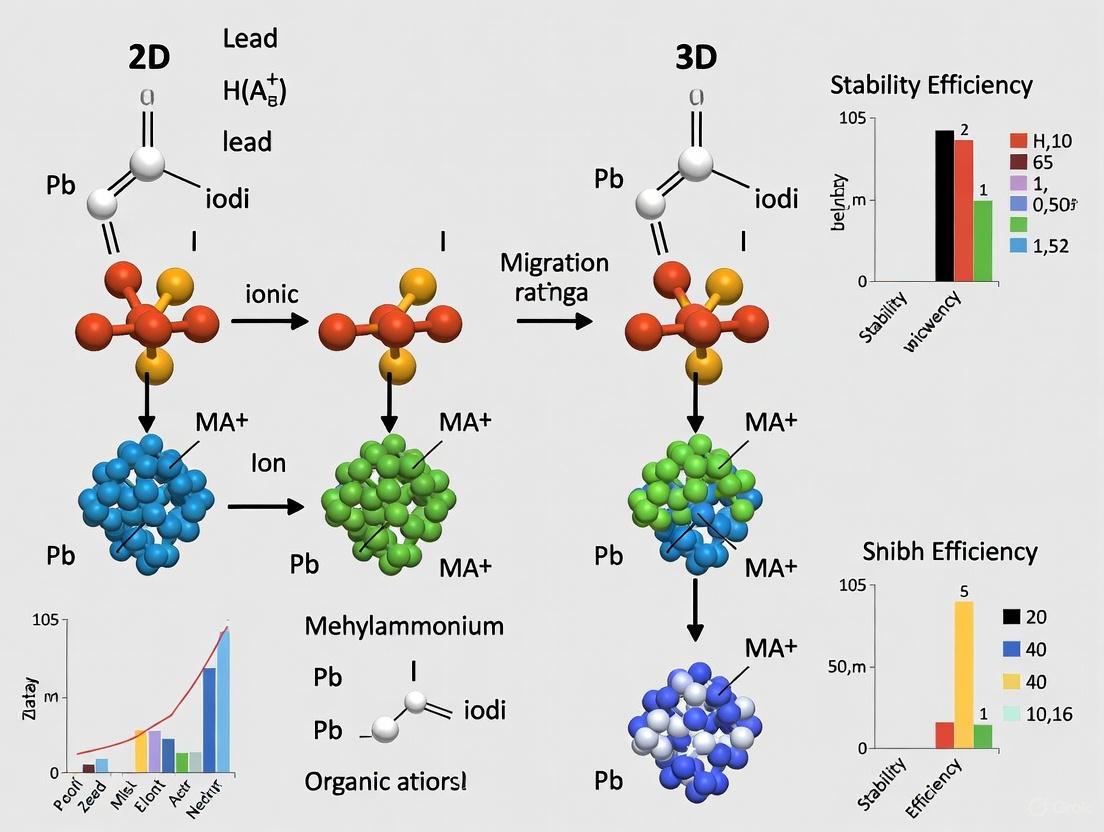
Ion Migration in 2D vs. 3D Perovskite Quantum Dots: Mechanisms, Impacts, and Strategies for Stable Optoelectronics
This article provides a comprehensive comparison of ion migration in two-dimensional (2D) and three-dimensional (3D) perovskite quantum dots (PQDs), a critical factor influencing the performance and operational stability of optoelectronic...
Ion Migration in 2D vs. 3D Perovskite Quantum Dots: Mechanisms, Impacts, and Strategies for Stable Optoelectronics
Abstract
This article provides a comprehensive comparison of ion migration in two-dimensional (2D) and three-dimensional (3D) perovskite quantum dots (PQDs), a critical factor influencing the performance and operational stability of optoelectronic devices. We explore the foundational mechanisms of ion migration, highlighting the distinct structural characteristics of 2D and 3D perovskites that lead to differences in activation energy and migration pathways. The review covers advanced methodological approaches for characterizing ion dynamics and analyzes its dual role as both a source of device degradation and a potential tool for novel applications like memristors. A core focus is troubleshooting and optimization, presenting strategies such as compositional engineering, surface ligand modification, and dimensional tuning to suppress detrimental ion migration. Finally, a direct comparative analysis validates the stability-performance trade-offs, offering insights for researchers and scientists to tailor material properties for enhanced device longevity, particularly in demanding fields like biomedical sensing and imaging.
Unraveling the Core Principles: Structural Origins of Ion Migration in Perovskite Lattices
The exploration of halide perovskites for optoelectronic applications has revealed a fundamental trade-off: while three-dimensional (3D) perovskites exhibit exceptional charge transport properties, their two-dimensional (2D) counterparts demonstrate superior environmental stability. This comparative analysis delves into the crystallographic foundations and defect chemistry underlying these performance characteristics, with particular focus on ionic migration. Understanding these structure-property relationships is crucial for designing next-generation perovskite quantum dot (QD) devices that balance efficiency with operational longevity. Research has increasingly focused on low-dimensional perovskite nanostructures, including QDs, to enhance material stability while maintaining favorable optoelectronic properties through quantum confinement effects [1].
Structural Fundamentals of 2D and 3D Perovskite Frameworks
Three-Dimensional (3D) Perovskite Structures
The canonical 3D perovskite structure follows the general formula ABX₃, where A is a monovalent cation (e.g., MA⁺, FA⁺, or Cs⁺), B is a divalent metal cation (typically Pb²⁺ or Sn²⁺), and X is a halide anion (I⁻, Br⁻, or Cl⁻) [2]. The crystal architecture consists of corner-sharing [BX₆]⁴⁻ octahedra that form an extended network, with A-site cations occupying the cuboctahedral cavities within this framework [3]. This connectivity creates a highly symmetric structure, most commonly in cubic or tetragonal phases, which enables efficient charge transport through orbital overlap across the inorganic framework [4].
The stability of the 3D perovskite structure is governed by the Goldschmidt tolerance factor (t) and octahedral factor (μ), which predict structural stability based on ionic radii [2]. The tolerance factor is calculated as t = (rA + rX) / [√2(rB + rX)], where rA, rB, and rX represent the ionic radii of the respective ions. For stable 3D perovskites, t typically falls between 0.81 and 1.11, while μ (calculated as rB/r_X) generally ranges from 0.44 to 0.90 to maintain stable [BX₆]⁴⁻ octahedra [2]. Deviations from these ranges often result in non-perovskite structures with diminished optoelectronic properties.
Two-Dimensional (2D) Perovskite Structures
In contrast to their 3D counterparts, 2D perovskites incorporate bulky organic spacer cations that slice the continuous 3D framework into discrete inorganic layers. The most common 2D perovskites belong to the Ruddlesden-Popper (RP) series with the general formula L₂Aₙ₋₁BₙX₃ₙ₊₁, where L represents a large organic ammonium spacer cation (e.g., phenylethylammonium (PEA) or butylammonium (BA)), and n indicates the number of inorganic octahedral layers between organic sheets [4] [5]. When n = 1, a pure 2D structure is formed, while n > 1 creates quasi-2D structures with varying degrees of quantum confinement [4].
The Dion-Jacobson (DJ) phase represents another important 2D perovskite family with the formula DAn-1MnX3n+1, where D is a divalent spacer cation [4]. These structures typically exhibit aligned octahedral layers with no relative shift, unlike the staggered configuration of RP phases [4]. A third category, alternating cations in the interlayer space (ACI) perovskites, feature (1/2, 0) shifts and incorporate guanidinium spacer cations alternating with small cations in the interlayer space [4]. The organic spacer cations in 2D perovskites serve as natural barriers to environmental degradation while simultaneously imposing quantum confinement effects that modify the electronic structure [6].
Table 1: Structural Classification of 2D Perovskite Families
| Perovskite Type | General Formula | Spacer Cation | Layer Offset | Key Characteristics |
|---|---|---|---|---|
| Ruddlesden-Popper (RP) | L₂Aₙ₋₁BₙX₃ₙ₊₁ | Monovalent (e.g., PEA⁺, BA⁺) | (1/2, 1/2) shift | Most commonly studied, easy exfoliation, bilayer organic spacing |
| Dion-Jacobson (DJ) | DAₙ₋₁BₙX₃ₙ₊₁ | Divalent (e.g., BDA²⁺, 4-AMP²⁺) | (0, 0) shift | Closer interlayer spacing, enhanced charge transport |
| Alternating Cations (ACI) | (GA)An-1BnX3n+1 | Guanidinium (GA⁺) | (1/2, 0) shift | Alternating cation arrangement, less common |
Defect Chemistry and Ion Migration Mechanisms
Defect Formation Energetics
The thermodynamic stability of perovskite structures directly influences their defect formation energetics. First-principles density functional theory (DFT) calculations reveal that equilibrium concentrations of point defects are significantly lower in 2D perovskites compared to their 3D counterparts [6]. For instance, the formation energy of lead vacancies (VPb²⁻) increases from 0.50 eV in MAPbI₃ to 0.82 eV in PEA₂PbI₄ and 1.16 eV in BA₂PbI₄ under intrinsic Fermi level conditions [6]. Similarly, iodine vacancy (VI⁺) formation energies rise from 0.61 eV in MAPbI₃ to approximately 1.14-1.15 eV in 2D analogues [6].
This enhanced defect formation energy in 2D structures originates from the more disruptive nature of bonding disruptions in the confined 2D network compared to the extended 3D framework [6]. When point defects do form in 2D perovskites, they often introduce deep trap states within the band gap that facilitate non-radiative recombination, contrasting with the predominantly shallow defects in 3D perovskites that contribute to their celebrated "defect tolerance" [6]. This fundamental difference in defect behavior has profound implications for optoelectronic performance and device stability.
Ion Migration Pathways
Ion migration represents a critical degradation mechanism in perovskite devices, contributing to current-voltage hysteresis, phase segregation, and overall performance degradation [7]. In 3D perovskites, halide ions can migrate through the continuous crystal lattice via vacancy-assisted mechanisms, with activation energies typically ranging from 0.1 to 0.5 eV depending on the specific composition [8]. This facile ion movement stems from the highly dynamic and relatively open structure of 3D frameworks.
In 2D perovskites, the organic spacer layers create natural barriers that suppress ion migration perpendicular to the inorganic layers [4]. Experimental studies on (BA₂PbI₄)ₓ(MAPbI₃)₁₋ₓ mixed-dimensional perovskites demonstrate that incorporating 2D phases significantly reduces ionic conductivity compared to pure 3D MAPbI₃ films [8]. The layered structure confines ion movement primarily to the two-dimensional plane of the inorganic layers, creating anisotropic migration pathways with higher energy barriers for cross-layer transport [6]. This suppressed ion migration directly correlates with improved operational stability in 2D perovskite devices under electrical bias [8].
Table 2: Comparative Defect and Ion Migration Properties
| Property | 3D Perovskites | 2D Perovskites | Experimental Evidence |
|---|---|---|---|
| Defect Formation Energy (V_Pb²⁻) | 0.50 eV (MAPbI₃) | 0.82 eV (PEA₂PbI₄), 1.16 eV (BA₂PbI₄) | DFT calculations [6] |
| Iodine Vacancy Formation | 0.61 eV (MAPbI₃) | 1.14-1.15 eV (2D analogues) | DFT calculations [6] |
| Ion Migration | Facile through 3D network | Suppressed by organic barriers | Reduced ionic conductivity in 2D-3D mixtures [8] |
| Defect Types | Predominantly shallow traps | Deep traps more common | Non-radiative recombination in 2D perovskites [6] |
| Equilibrium Defect Concentration | Higher | Lower by several orders of magnitude | Thermodynamic calculations [6] |
Experimental Methodologies for Characterization
Computational Approaches
First-principles density functional theory (DFT) calculations provide fundamental insights into defect thermodynamics and electronic structure. Standard methodology involves using packages such as the Vienna Ab Initio Simulation Package (VASP) with appropriate functionals (e.g., SCAN+rVV10) for accurate defective structures and total energies [6]. Calculations typically employ 3×3×3 supercells for cubic systems and 2×2×1 supercells for orthorhombic structures, with k-point sampling adjusted accordingly [3] [6]. Defect formation energies (DFEs) are calculated using the standard formalism: ΔHf = Etotal(defect) - Etotal(perfect) - Σniμi + q(EF + EVBM), where Etotal represents total energies, ni and μi are the number and chemical potential of species i, q is the defect charge, EF is the Fermi level, and EVBM is the valence band maximum [6]. Charge-state transition levels (CSTLs) identify trap states within the band gap by evaluating the Fermi level position where charge states have equal formation energies [6].
Electrical Characterization Techniques
Direct electrical measurements probe ion migration and charge transport dynamics in perovskite materials. Vertical device structures allow analysis of current-density-voltage (J-V) characteristics, revealing ion migration through hysteresis and ideality factor variations [8]. Temperature-dependent J-V measurements (typically 200-300 K range) extract activation energies for ion migration and charge transport [8].
Lateral device configurations with symmetric electrodes enable direct quantification of ionic and electronic conductivities through DC galvanostatic polarization measurements [8]. This method applies a constant current bias and monitors voltage transients, separating ionic and electronic contributions based on their characteristic response times. Hall effect measurements using the van der Pauw configuration provide complementary data on charge carrier concentration and mobility [8].
Nanoscale Microscopy Techniques
Conductive atomic force microscopy (C-AFM) maps local conductivity variations with nanoscale resolution, typically using Pt/Ir-coated tips under controlled atmospheric conditions [8]. This technique reveals how different crystalline phases and grain boundaries influence charge transport in mixed-dimensional perovskites.
Kelvin probe force microscopy (KPFM) measures surface potential distributions and work function variations, operating in non-contact mode with an applied alternating current voltage (typically 1.0 V at 70 kHz) [8]. KPFM visualizes surface photovoltage (SPV) responses under illumination, identifying band bending and charge segregation at interfaces between different perovskite phases [8].
Research Reagent Solutions and Materials
Table 3: Essential Research Reagents for Perovskite Quantum Dot Studies
| Reagent/Material | Function | Application Examples |
|---|---|---|
| Lead Iodide (PbI₂) | Pb²⁺ source for inorganic framework | Precursor for both 2D and 3D perovskite synthesis [8] |
| Methylammonium Iodide (MAI) | A-site cation for 3D perovskites | Formation of MAPbI₃ precursor solutions [8] |
| Cesium Precursors (e.g., CsI, Cs₂CO₃) | Inorganic A-site cation source | Synthesis of all-inorganic CsPbI₃ QDs [2] |
| Spacer Cations (PEAI, BAI) | Organic layers for 2D perovskites | Creating Ruddlesden-Popper phases [8] [5] |
| Solvents (DMF, DMSO) | Precursor dissolution | Preparing perovskite precursor solutions [8] |
| Antisolvents (Chlorobenzene, Toluene) | Crystallization control | Inducing rapid supersaturation during spin-coating [8] |
| Capping Ligands (Oleic Acid, Oleylamine) | Surface passivation & size control | Stabilizing QDs in colloidal suspensions [2] [1] |
Structural and Defect Workflow
The experimental and computational approaches for investigating perovskite structure-defect relationships involve multiple interconnected methodologies, as visualized below:
The crystalline architecture of perovskite materials fundamentally governs their defect chemistry and ion migration behavior. Three-dimensional perovskites offer superior charge transport but suffer from higher defect concentrations and facile ion migration. Two-dimensional counterparts provide enhanced stability through reduced defect densities and suppressed ion migration, albeit at the cost of anisotropic charge transport. These competing attributes necessitate careful dimensional engineering for specific optoelectronic applications. Mixed-dimensional 2D-3D systems and perovskite quantum dots represent promising avenues for balancing these competing factors, leveraging the stability of 2D structures with the efficient charge transport of 3D frameworks. Future research should focus on precise control of phase distribution, interface engineering, and advanced passivation strategies to further suppress deep-level defects while maintaining efficient charge extraction.
Ionic migration is a fundamental phenomenon in metal halide perovskites that significantly influences the performance and operational stability of optoelectronic devices. In the context of perovskite quantum dots (QDs), this process involves the movement of halide anions (I⁻, Br⁻, Cl⁻) and A-site cations (Cs⁺, MA⁺, FA⁺) through the crystal lattice under external stimuli such as electric fields, light, or heat [9] [10]. The identification of which ions move and through what pathways is crucial for designing stable, high-performance materials for applications ranging from photovoltaics to memory devices and light-emitting diodes. While three-dimensional (3D) perovskites exhibit pronounced ionic migration that often leads to device degradation, emerging research demonstrates that low-dimensional perovskites, particularly two-dimensional (2D) and quasi-2D structures, offer innovative pathways to suppress these detrimental movements through structural engineering at the molecular level [5] [4]. This comparative analysis examines the mobile ions and their migration pathways in 2D versus 3D perovskite quantum dots, providing a structured framework for understanding and controlling these processes in advanced optoelectronic applications.
Comparative Analysis: Ionic Migration in 2D vs. 3D Perovskite QDs
Table 1: Fundamental Characteristics of Ionic Migration in 2D vs. 3D Perovskite QDs
| Characteristic | 3D Perovskite QDs | 2D/Quasi-2D Perovskite QDs |
|---|---|---|
| Primary Mobile Ions | Halides (I⁻, Br⁻), A-site cations (MA⁺, FA⁺, Cs⁺) [9] [10] | Primarily halides, with cations restricted by organic spacers [5] [4] |
| Migration Pathways | Continuous networks through crystal lattice, grain boundaries [10] | Limited to inorganic layers; blocked by organic spacers in out-of-plane direction [5] [4] |
| Activation Energy for Migration | Lower activation energy barriers [10] | Higher activation energy due to structural confinement [4] |
| Impact on VLC Performance | Reduces data rates, 90 Mbps achieved with OOK modulation [9] | Improved stability maintains performance over time [4] |
| Role in Memory Devices | Forms conductive filaments for resistive switching [10] | Suppressed migration enables more controlled switching [10] |
| Stabilization Strategies | Compositional engineering, surface passivation [11] | Built-in organic spacers, multidimensional structures [5] [4] |
Table 2: Quantitative Comparison of Migration Effects and Stability Metrics
| Parameter | 3D Perovskite QDs | 2D/Quasi-2D Perovskite QDs | Measurement Technique |
|---|---|---|---|
| Data Rate in VLC | 90 Mbps (OOK modulation) [9] | Information not available in search results | On-off keying modulation |
| Photoluminescence Retention | Varies with composition and stress conditions | >95% PLQY after 30 days at 60% RH [11] | Steady-state PL spectroscopy |
| Environmental Stability | Degradation in ambient conditions [5] | Stable luminescence at 80% humidity for 50 days [12] | Luminescence monitoring in controlled environments |
| Ion Migration Contribution to Hysteresis | Significant [10] | Suppressed [4] | Current-voltage (I-V) characterization |
| Device Operational Lifetime | Limited by ion migration [9] | Enhanced T50 > 130 hours [13] | Accelerated aging tests |
Experimental Protocols for Studying Ionic Migration
Ion Migration Realization and Measurement
The experimental investigation of ion migration in perovskite systems requires carefully designed protocols to isolate and quantify these processes. One established methodology involves creating mixed halide perovskite systems to track halide migration through optical and electrical measurements. As demonstrated in VLC research, mixing CsPbBr₃ and CsPbI₃ quantum dots creates a system where halide ion migration can be directly observed through changes in photoluminescence (PL) lifetime and shifts in emission spectra [9]. During the migration process, the performance of the VLC system is temporarily reduced but typically returns to its initial state after stabilization, indicating the dynamic nature of ionic movements and their redistribution within the perovskite structure.
The characterization of these phenomena employs multiple complementary techniques. Transient photoluminescence spectroscopy (TRPL) provides insights into recombination dynamics affected by mobile ions, with lifetime variations serving as indicators of migration extent [9] [13]. X-ray diffraction (XRD) analysis reveals structural changes and phase segregation resulting from ion migration, while X-ray photoelectron spectroscopy (XPS) offers surface chemical information and defect states that facilitate ionic movement [11]. Electrical characterization through current-voltage (I-V) measurements with varying sweep rates and directions can detect hysteresis phenomena directly attributable to ion migration, with the magnitude of hysteresis serving as a qualitative indicator of migration extent [10].
Advanced Characterization Techniques
Beyond fundamental realization of ion migration, advanced characterization methods provide deeper insights into migration pathways and kinetics. Density Functional Theory (DFT) calculations complement experimental studies by quantifying binding energies between ions and the perovskite lattice, revealing potential migration barriers and pathways [13]. For instance, DFT has been used to calculate the binding energies of ionic liquids with perovskite QD surfaces, demonstrating strong coordination (e.g., -1.49 eV between OTF⁻ and Pb²⁺) that effectively suppresses ion migration [13].
Time-resolved electrical measurements offer another powerful approach, particularly for evaluating the dynamic response of perovskite-based devices. In light-emitting diode applications, the rise time of electroluminescence (EL) response serves as an indicator of defect-mediated processes including ion migration. Studies have shown that passivation strategies which reduce defect states can decrease EL rise time by over 75%, demonstrating a direct correlation between ionic movement and device performance [13]. Impedance spectroscopy further complements these methods by quantifying ionic and electronic contributions to conductivity across different frequency domains, enabling the calculation of activation energies for ion migration through Arrhenius analysis.
Ion Migration Study Workflow
The Scientist's Toolkit: Essential Research Reagents and Materials
Table 3: Key Research Reagents for Ionic Migration Studies
| Reagent/Material | Function in Migration Studies | Representative Application |
|---|---|---|
| CsPbBr₃/CsPbI₃ QD Mixtures | Enables visualization of halide migration through spectral changes [9] | VLC system performance analysis during ion migration [9] |
| Organic Spacer Cations (BA⁺, PEA⁺) | Creates structural barriers to ion migration in 2D perovskites [5] [4] | Enhancing environmental stability in humid conditions [12] |
| Ionic Liquids ([BMIM]OTF) | Passivates surface defects and suppresses ion migration [13] | Improving response speed and stability of PeLEDs [13] |
| Carbon Quantum Dots (CQDs) | Passivates defects via H-bond interactions, reducing migration pathways [12] | Enhancing water stability of quasi-2D perovskites [12] |
| Mixed Halide Compositions | Allows tracking of anion migration through halide exchange [9] | Investigating migration pathways and kinetics [9] |
Migration Pathways and Structural Influences
The structural architecture of perovskite materials fundamentally determines the pathways available for ionic migration, creating stark contrasts between 3D and 2D configurations.
Ion Migration Pathways Comparison
In 3D perovskite QDs, the corner-sharing [PbX₆] octahedra form a continuous network that provides low-energy pathways for both halide anions and A-site cations [10]. This interconnected structure allows multi-directional ion migration through vacancies and interstitials within the lattice, with additional fast migration channels along grain boundaries and surfaces. The relatively open crystal framework results in lower activation energies for ion movement, making 3D perovskites particularly susceptible to field-driven ion redistribution that manifests as current-voltage hysteresis, phase segregation, and operational instability in devices [9] [10].
Conversely, 2D and quasi-2D perovskite QDs incorporate bulky organic spacer cations (such as BA⁺ or PEA⁺) that slice the continuous 3D network into discrete inorganic layers separated by these organic barriers [5] [4]. This architectural modification fundamentally alters migration pathways, constraining ion movement primarily within the two-dimensional inorganic sheets while effectively blocking out-of-plane migration through the organic layers. The natural quantum well structure in 2D perovskites creates higher activation energy barriers for ion migration, significantly suppressing these processes and enhancing operational stability [4] [12]. This structural advantage makes 2D perovskite QDs particularly valuable for applications requiring long-term stability, such as commercial displays and lighting systems where consistent performance is essential.
The systematic comparison of ionic migration in 2D versus 3D perovskite quantum dots reveals fundamental differences in mobile ion species, migration pathways, and resultant device implications. While 3D perovskite QDs offer simplicity in synthesis and excellent initial optoelectronic properties, their susceptibility to ion migration presents significant challenges for long-term device stability. Conversely, 2D and quasi-2D perovskite QDs, through their incorporated organic spacers, create natural barriers that constrain ion movement and enhance operational resilience without compromising performance. The experimental methodologies and reagent solutions outlined in this analysis provide researchers with standardized approaches for quantifying and controlling these migration processes. As perovskite technologies advance toward commercial applications, understanding and engineering ionic migration through dimensional control will remain crucial for developing next-generation optoelectronic devices with combined high performance and exceptional stability.
Ion migration, particularly of halide ions like iodide (I⁻), is a primary factor degrading the long-term performance and stability of perovskite optoelectronic devices [4] [14]. This process, accelerated by light, heat, and electrical bias, leads to material decomposition, interfacial reactions, and disruption of the electric-field distribution within the device [14]. The activation energy (Eₐ) for ion migration represents the minimum energy barrier that must be overcome for ions to move through the crystal lattice, serving as a critical quantitative metric for assessing and improving material stability [8] [14].
Research has demonstrated that two-dimensional (2D) and 2D-3D mixed perovskite systems can significantly suppress ion migration compared to their three-dimensional (3D) counterparts, leading to enhanced device durability [4] [5]. This guide provides a comparative analysis of ionic migration in 2D and 3D perovskite systems, focusing on quantified energy barriers, experimental methodologies for their determination, and the material solutions that leverage these principles to achieve breakthrough device stability.
Comparative Analysis of Migration Barriers in 2D and 3D Perovskites
Quantified Barrier Energy in 3D Perovskites
In standard 3D perovskite solar cells (PSCs) based on FAPbI₃, the threshold barrier energy required to prevent the loss of iodide ions from the perovskite film into the hole transport layer (HTL) has been quantitatively determined. Recent research established this barrier at 0.911 eV, achieved by applying a reverse bias to create a sufficient potential drop in the depletion region that counteracts ion diffusion and drift [14]. This quantitative finding provides a crucial benchmark for developing effective blocking strategies.
Enhanced Stability in 2D and 2D-3D Systems
Mixed-dimensional 2D-3D perovskite structures exhibit markedly improved stability against ion migration compared to pure 3D perovskites [8] [5]. The enhanced stability originates from several intrinsic properties of the 2D components:
- Structural Confinement: The incorporation of bulky organic spacer cations (e.g., BA⁺, PEA⁺) creates a natural barrier to ion movement, effectively increasing the activation energy for migration [4] [5].
- Defect Passivation: 2D perovskites formed at the surface or grain boundaries of 3D perovskites can passivate interfacial trap states, which are common pathways for ion migration [8] [5].
- Stress Relaxation: The 2D components help relax residual stress in the perovskite microstructure, reducing the additional driving force for ion migration [8].
Table 1: Comparative Analysis of Ionic Migration in 2D and 3D Perovskite Systems
| Characteristic | 3D Perovskites (e.g., MAPbI₃, FAPbI₃) | 2D-3D Mixed Perovskites | Pure 2D Perovskites (n=1) |
|---|---|---|---|
| Typical Formulations | MAPbI₃, FAPbI₃, mixed cation/halide [5] | (BA₂PbI₄)ₓ(MAPbI₃)₁₋ₓ, (PEA)₂(MA)ₙ₋₁PbₙI₃ₙ₊₁ [8] [5] | BA₂PbI₄, PEA₂PbI₄ [8] |
| Barrier to Ion Migration | Low intrinsic barrier; quantified suppression requires ~0.911 eV external barrier [14] | High intrinsic barrier due to structural confinement and defect passivation [8] [4] | Very high barrier; extremely stable but poor charge transport [4] [5] |
| Key Stabilization Mechanism | External blocking layers (e.g., HfO₂, dipole monolayers) [14] | Internal structural blocking by organic spacers and interface engineering [8] [5] | Complete separation of inorganic layers by hydrophobic organic cations [4] |
| Impact on Charge Transport | High carrier mobility, but ion migration degrades interfaces over time [5] [14] | Balanced transport and stability; restricted charge transport at 2D-3D heterojunction possible [8] | Low carrier mobilities, high anisotropy; unfavorable for efficient devices [4] [5] |
| Stability Performance | Poor long-term stability; degrades under heat, light, and humidity [5] [14] | Highly improved stability; devices maintain >95% initial PCE after 1500h at 85°C [14] | Extremely high environmental stability [4] [5] |
Experimental Protocols for Quantifying Ion Migration
Quantifying the Barrier Energy Threshold
A pivotal 2025 study established a protocol to precisely quantify the barrier energy needed to suppress iodide migration [14]:
- Principle: Iodide ions migrate due to diffusion (concentration gradient) and drift (built-in electric field). A reverse bias applied to the device increases the potential drop in the depletion region, enhancing the drift component. The threshold barrier energy is the potential drop at which drift and diffusion reach dynamic equilibrium, confining iodide ions.
- Procedure:
- Device Aging & Bias Application: Age perovskite solar cells (e.g., FAPbI₃/PTAA) under illumination while applying a series of reverse biases.
- Interface Analysis with XPS: Use X-ray photoelectron spectroscopy (XPS) to monitor the presence of Iodine (I 3d peaks) at the HTL (PTAA) surface after aging.
- Identify Equilibrium Bias: Determine the specific reverse bias voltage (e.g., -0.8 V for FAPbI₃) at which Iodine signals disappear from the HTL surface, indicating successful confinement.
- Calculate Potential Drop: Calculate the corresponding potential drop within the HTL depletion region under the identified bias (e.g., 0.911 V for FAPbI₃), which equals the required barrier energy.
This method was validated for multiple compositions (FAPbI₃, FA₀.₉MA₀.₁PbI₃, FA₀.₉Cs₀.₁PbI₃, FA₀.₉MA₀.₀₅Cs₀.₀₅PbI₃), yielding specific barrier energies for each [14].
Characterizing Local Ionic and Electronic Behavior
Advanced microscopy techniques are essential for understanding localized migration phenomena and electronic properties in 2D-3D mixed films [8]:
- Conductive Atomic Force Microscopy (C-AFM): Measures nanoscale conductive current-voltage (J-V) characteristics, mapping local variations in conductivity and their correlation to different perovskite phases (2D, 3D) and grain boundaries.
- Kelvin Probe Force Microscopy (KPFM): Maps the surface potential distribution and work function, allowing analysis of band bending and surface photovoltage (SPV) response across grains and grain boundaries with different phases.
Table 2: Key Research Reagent Solutions and Experimental Materials
| Material / Reagent | Function / Role | Application Context |
|---|---|---|
| n-butylammonium iodide (BAI) | Precursor for introducing 2D perovskite phase (BA₂PbI₄) [8] | Fabrication of (BA₂PbI₄)ₓ(MAPbI₃)₁₋ₓ mixed perovskite films [8] |
| Phenethylammonium iodide (PEA) | Precursor for introducing 2D perovskite phase (PEA₂PbI₄) [5] | Fabrication of (PEA)₂(MA)ₙ₋₁PbₙI₃ₙ₊₁ Ruddlesden-Popper perovskites [5] |
| Hafnium Oxide (HfO₂) | Atomic-layer-deposited scattering barrier to block iodide ions [14] | Used as part of a composite blocking layer on 3D perovskite surfaces (e.g., FAPbI₃) [14] |
| CF3-PBAPy Molecule | Forms an ordered dipole monolayer creating a drift electric-field barrier [14] | Self-assembles on HfO₂ layer to provide additional ~0.6 eV energy barrier against ion migration [14] |
| Poly(N-vinylcarbazole) (PVK) | Hole transport material (HTM) with high work function [14] | Mitigates band shift induced by interfacial electric-fields in devices with blocking layers [14] |
| PTAA (PTAA) | Common polymeric hole transport material [14] | Used as the HTL in model systems for quantifying iodide migration and barrier energy [14] |
Visualization of Experimental Workflows and Material Architectures
Workflow for Barrier Energy Quantification
The following diagram illustrates the experimental and calculation process for determining the threshold barrier energy to suppress iodide migration.
Architecture of a Composite Blocking Layer
This diagram outlines the structure and functional principles of a composite layer designed to meet the quantified barrier energy requirement on a 3D perovskite surface.
Performance Data and Stability Outcomes
Efficacy of Engineered Barriers in 3D Systems
Implementing the quantified barrier approach in 3D perovskite solar cells leads to exceptional performance and stability, as shown in the table below.
Table 3: Performance and Stability Data for 3D PSCs with Engineered Barriers
| Parameter | Control Device (No dedicated barrier) | With Composite Blocking Layer (HfO₂ + CF3-PBAPy) | Measurement Conditions |
|---|---|---|---|
| Power Conversion Efficiency (PCE) | ~25% (typical for high-performance devices) | 25.86% (Certified steady-state: 25.70%) [14] | Standard 1-sun illumination [14] |
| Iodide Migration Suppression | Baseline | Reduction by 99.9% compared to control [14] | TOF-SIMS/XPS analysis after aging [14] |
| Operational Stability (T85) | Significant degradation | >95% of initial PCE retained [14] | 1500 hours at 85°C under maximum power point tracking [14] |
| Damp-Heat Stability (D85) | Significant degradation | No significant efficiency degradation [14] | 1000 hours at 85°C / 85% Relative Humidity [14] |
Stability Performance of 2D-3D Systems
The stability benefits of incorporating 2D components are well-documented, though peak efficiencies can be slightly lower than optimized 3D systems.
- Unencapsulated Stability: 2D-3D perovskite hybrid films (e.g., CA₂PbI₄/MAPbIₓCl₃₋ₓ) showed no degradation after 40 days in high humidity (63 ± 5%), while pristine 3D perovskite degraded significantly [5].
- High-Efficiency Devices: Using 2-thiophenemethylammonium (ThMA) as a spacer cation in a 2D-3D structure resulted in a PCE of ~21.49% and high operational stability, achieved by passivating trap states and hindering ion motion [5].
- Long-Term Stability: Engineering a 2D/3D ((HOOC(CH₂)₄NH₃)₂PbI₄/CH₃NH₃PbI₃) perovskite junction yielded a device that showed minimal degradation over one year [5].
Quantifying the activation energy for ion migration provides a powerful, targeted framework for enhancing perovskite stability. For 3D perovskite systems, this has led to the precise engineering of composite blocking layers that meet a quantified energy barrier (~0.911 eV for FAPbI₃), resulting in a dramatic suppression of iodide migration (99.9%) and record-setting operational stability [14]. For 2D and 2D-3D mixed-dimensional systems, the enhanced stability is intrinsically linked to a higher inherent activation energy barrier for ion migration, provided by the structural confinement of bulky organic cations and superior defect passivation [8] [4] [5].
The choice between optimizing 3D systems with engineered barriers or utilizing 2D-3D mixtures involves a trade-off between the ultimate efficiency potential of 3D systems and the superior intrinsic stability and processability of 2D-3D systems. Future research will likely focus on further refining the quantification of migration barriers in diverse 2D-3D compositions and leveraging this understanding to design novel material architectures that push the boundaries of both efficiency and long-term device stability.
Influence of Quantum Confinement and Dielectric Effects on Ion Mobility
The commercialization of perovskite-based optoelectronic devices is critically dependent on overcoming instability issues, a significant source of which is ion migration. This review provides a comparative analysis of ionic migration in three-dimensional (3D) perovskites versus low-dimensional perovskites, with a specific focus on the fundamental roles played by quantum confinement and dielectric confinement. While 3D perovskites offer superior charge transport, their inherent instability and pronounced ion migration remain primary concerns [15]. Low-dimensional perovskites, particularly quasi-2D structures and quantum dots (QDs), introduce unique physical constraints that effectively suppress ion mobility, thereby presenting a promising pathway toward enhanced device longevity and performance [4].
Fundamental Concepts: Confinement Effects in Perovskites
Quantum Confinement and Dielectric Confinement
The optoelectronic properties of low-dimensional perovskites are governed by two principal effects: quantum confinement and dielectric confinement.
Quantum Confinement: This effect arises when the physical dimensions of the perovskite crystal (e.g., the thickness of the inorganic slab in 2D materials or the overall size of a quantum dot) become comparable to or smaller than the Bohr exciton radius. This spatial restriction leads to a discretization of energy levels and a widening of the bandgap [16] [17]. In 2D Ruddlesden-Popper (RP) perovskites, the number of inorganic octahedral layers, denoted by the value
n, directly determines the degree of quantum confinement, with lowernvalues resulting in stronger confinement [18] [17].Dielectric Confinement: This effect stems from the significant difference in dielectric constants between the inorganic semiconductor layers (high dielectric constant) and the intervening organic spacer layers (low dielectric constant) [17]. This dielectric mismatch enhances the Coulombic attraction between photogenerated electrons and holes. The force of this attraction is inversely proportional to the square of the distance and the dielectric constant (F = -e²/4πεr²) [17]. The reduced dielectric screening in the organic regions leads to a massive increase in exciton binding energy (Eb). The binding energy in a 2D quantum-well structure can be expressed as Eb^(2D+ε) = 4(ε_w/ε_b)² Eb^(3D), where εw and εb are the dielectric constants of the well and barrier, respectively [17]. This is visually summarized in the diagram below.
Structural Classifications of 2D and Quasi-2D Perovskites
Low-dimensional perovskites are categorized based on their crystalline structure and the nature of the organic spacer cations. The three primary phases are:
- Ruddlesden-Popper (RP) Phase: This phase employs monovalent organic spacer cations (e.g., phenylethylammonium (PEA), butylammonium (BA)) and is characterized by a bilayer of these cations between inorganic slabs, introducing van der Waals gaps [4] [15].
- Dion-Jacobson (DJ) Phase: This phase utilizes divalent organic spacer cations (e.g., 4-aminomethylpiperidinium (4-AMP)), leading to a more compact and direct connection between inorganic layers without van der Waals gaps, which often enhances structural stability [4] [15].
- Alternating Cations in the Interlayer (ACI) Phase: This phase features a unique structure where different cations, such as guanidinium (GA), alternate within the interlayer space [18] [17].
The following diagram illustrates the structural mechanisms through which these phases influence ion mobility.
Comparative Analysis: Ion Mobility in 2D/Quasi-2D vs. 3D Perovskites
The structural differences between 3D, 2D, and quasi-2D perovskites directly translate to distinct ion migration behaviors. The following table provides a quantitative and qualitative comparison based on recent experimental findings.
Table 1: Comparative Analysis of Ion Mobility in 3D, 2D, and Quasi-2D Perovskites
| Property | 3D Perovskites (e.g., MAPbI₃) | 2D/Quasi-2D Perovskites | Experimental Evidence & Data |
|---|---|---|---|
| Ion Migration Rate | High | Significantly Suppressed | Unencapsulated Tyr-optimized quasi-2D devices retained 96% of initial efficiency after 2,186 hours at 45% ± 5% relative humidity (RH), demonstrating drastically reduced ion migration-induced degradation [18]. |
| Thermal Stability | Poor; significant degradation at 85°C | Greatly Enhanced | Devices with stabilized low-n phases retained 88% of initial efficiency after 500 hours at 85°C, compared to ~60% for the control group, indicating higher activation energy for ion migration [18]. |
| Structural Mechanism | Continuous ionic pathways along grain boundaries | Organic spacers act as physical barriers, disrupting ion migration pathways [4]. | The insertion of spacer cations (e.g., Tyrosine) between inorganic slabs increases the activation energy for ion migration [18] [4]. |
| Grain Boundary Density | High in polycrystalline films, facilitating ion migration | Ultra-large grains (3–5 μm) and improved crystallinity reduce grain boundary density [18]. | Films with tyrosine additive showed a 4-fold improvement in electron mobility and carrier diffusion length exceeding 1 μm, consistent with reduced ionic scattering and trapping [18]. |
| Electronic Performance | High carrier mobility but compromised by ionic screening and hysteresis | Lower inherent mobility but minimized hysteresis and non-radiative losses. | The optimized charge transport in tyrosine-mediated films enabled a certified 20.28% efficiency for a large-area (72.47 cm²) module, proving scalability without significant ion migration losses [18]. |
Experimental Protocols for Probing Ion Mobility
To quantitatively assess ion mobility in perovskite materials, researchers employ a suite of advanced characterization techniques. The workflow for a comprehensive investigation is outlined below.
Detailed Methodologies
Hysteresis Analysis in Current-Voltage (J-V) Measurements:
- Protocol: Measure J-V curves at different scan rates (e.g., from 0.1 to 1.0 V/s). A strong dependence of the power conversion efficiency (PCE) on the scan rate indicates significant ion migration and capacitive effects. Devices with suppressed ion mobility exhibit minimal hysteresis and low scan-rate dependence [10].
- Application: The champion quasi-2D solar cell with tyrosine additive achieved a record 22.14% efficiency with "minimal hysteresis," directly indicating reduced ionic interference [18].
Temperature-Dependent Impedance Spectroscopy:
- Protocol: Measure the complex impedance of the device over a frequency range (e.g., 1 Hz to 1 MHz) at various temperatures. The resulting Nyquist plots are fitted with an equivalent circuit model. The ion migration activation energy (Ea) is extracted from the Arrhenius plot of the ionic conductivity (σi) using the equation: *σi T = σ₀ exp(-Ea / kBT)*, where T is temperature and kB is the Boltzmann constant [10].
- Application: This method directly quantifies the energy barrier for ion movement, which is increased in 2D structures due to the physical barrier of organic spacers [4].
Operational and Environmental Stability Testing:
- Protocol: Track the device's performance (PCE, Voc, Jsc, FF) under continuous illumination (operational stability), elevated temperature (e.g., 85°C thermal stability), or controlled humidity (e.g., 45-85% RH). The time until the performance drops to 80% of its initial value (T80) is a key metric.
- Application: As shown in Table 1, the superior stability of quasi-2D devices under heat and humidity is direct evidence of suppressed ion migration and structural degradation [18] [4].
The Scientist's Toolkit: Essential Reagents and Materials
The following table lists key materials and reagents crucial for synthesizing low-dimensional perovskites with controlled ion mobility, based on the protocols cited in the research.
Table 2: Key Research Reagent Solutions for Low-Dimensional Perovskite Studies
| Reagent/Material | Function | Example from Literature |
|---|---|---|
| Guanidinium Iodide (GAI) | Small A-site cation in quasi-2D perovskite precursor formulation. Forms part of the inorganic lattice [18]. | Used in (GA)(MA)ₙ₋₁PbₙI₃ₙ₊₁ quasi-2D perovskite precursors [18]. |
| Tyrosine Hydroiodide (Tyr) | Multifunctional additive for phase regulation. Coordinates with GA cations and [PbI₄]²⁻ octahedra via H-bonding and cation-π interactions, selectively stabilizing low-n phases and enhancing interlayer charge coupling [18]. |
Added to the perovskite precursor solution, increasing low-n phase (n ≤ 3) content from 5.67% to 36.72% [18]. |
| Phenylethylammonium (PEA) Iodide | Monovalent bulky organic spacer cation for forming Ruddlesden-Popper (RP) phase 2D perovskites [4]. | A standard spacer cation for creating (PEA)₂(MA)ₙ₋₁PbₙI₃ₙ₊₁ 2D/Quasi-2D films [4]. |
| 1,4-Butyldiammonium (BDA) Iodide | Divalent bulky organic spacer cation for forming Dion-Jacobson (DJ) phase 2D perovskites, leading to a more compact and stable structure [4]. | Used for creating BDA(MA)ₙ₋₁PbₙI₃ₙ₊₁ perovskites with improved structural stability [4]. |
| Methylammonium Bromide (MABr) | Source of small A-site cation and halide for synthesizing 3D and quasi-2D perovskite quantum dots (PQDs) [19]. | Reacted with PbBr₂ to synthesize CH₃NH₃PbBr₃ PQDs via ligand-assisted reprecipitation (LARP) or hot-injection methods [19]. |
| Oleic Acid & Oleylamine | Surface ligands/capping agents during PQD synthesis. Passivate surface defects, control crystal growth, and improve colloidal stability [19]. | Standard ligands used in the synthesis of CH₃NH₃PbBr₃ PQDs to achieve high photoluminescence quantum yields (PLQYs >95%) [19]. |
The strategic incorporation of low-dimensional architectures, specifically quasi-2D phases and quantum dots, presents a highly effective solution for suppressing ion migration in metal halide perovskites. The confinement effects—quantum confinement tailoring electronic properties and dielectric confinement enhancing exciton stability—are complemented by the physical barrier effect of bulky organic spacers. These spacers increase the activation energy for ion hopping and disrupt continuous migration pathways. As evidenced by superior thermal and environmental stability metrics, this approach successfully decouples the trade-off between operational stability and high efficiency. Future research should focus on the precise atomic-level engineering of spacer molecules and interface design to further minimize ionic losses while maximizing charge transport, ultimately paving the way for the commercial viability of perovskite-based optoelectronics.
Probing the Dynamics: Characterization Techniques and Application-Specific Consequences
The investigation of ionic migration in perovskite materials, particularly in the context of 2D versus 3D perovskite quantum dots, requires characterization techniques capable of probing nanoscale phenomena. Conductive Atomic Force Microscopy (C-AFM), Kelvin Probe Force Microscopy (KPFM), and DC Polarization have emerged as powerful tools for mapping and understanding charge transport, surface potential, and ion migration at the relevant length scales for these materials [20] [8]. These techniques provide complementary insights into the fundamental behaviors that govern perovskite performance and stability, bridging the gap between macroscopic device measurements and nanoscale material properties.
For researchers comparing ionic migration in 2D and 3D perovskite quantum dots, these tools offer distinct advantages. 2D perovskites, with their general formula L₂Aₙ₋₁BₙX₃ₙ₊₁ where L is an organic cation and n represents the number of inorganic layers, exhibit higher environmental stability but lower carrier mobilities compared to their 3D counterparts [4] [8]. Conversely, 3D perovskites (ABX₃) demonstrate high charge mobilities and excellent optoelectronic properties but suffer from poor stability and significant ion migration under operational fields [8]. Mixed-dimensional 2D-3D perovskites aim to combine these advantages, though the restricted charge transport at heterojunction interfaces remains a challenge [8].
Tool Fundamentals: Principles and Capabilities
Conductive Atomic Force Microscopy (C-AFM)
C-AFM operates by maintaining a conductive tip in contact with the sample surface while applying a voltage and measuring the resulting current. This technique maps local conductivity variations with nanoscale resolution, typically using Pt/Ir-coated cantilevers with force constants of approximately 1 N/m to ensure good electrical contact while minimizing surface damage [8]. The tip is grounded, and current measurements are conducted through a single terminal, allowing direct correlation of topographic features with conductive properties [8]. For perovskite studies, C-AFM effectively identifies current pathways through different crystalline phases and detects variations at grain boundaries where ion migration often initiates.
Kelvin Probe Force Microscopy (KPFM)
KPFM measures the contact potential difference (CPD) between a conductive AFM tip and the sample surface without physical contact, operating in non-contact mode with an applied AC voltage (typically 1-70 kHz) [8] [21]. The technique nullifies electrostatic forces between tip and sample by applying a DC bias voltage equal to the CPD, which directly relates to the sample's local work function [21] [22]. For investigating perovskites, KPFM reveals surface potential distributions influenced by composition, doping, and charge trapping, enabling visualization of band bending at grain boundaries and 2D-3D interfaces [8]. Advanced implementations like G-Mode KPFM capture dynamic electric phenomena with temporal resolution significantly faster than the cantilever bandwidth (e.g., 66 μs) [21].
DC Polarization
DC polarization techniques apply a constant voltage or current to the material and monitor the resulting current or voltage over time, providing insights into ionic and electronic conductivity contributions [8] [23]. In lateral device configurations, DC galvanostatic polarization measurements quantify these conductivities separately by analyzing the transient and steady-state responses [8]. When combined with AFM, DC polarization uses the tip as a nanoscale electrode to induce localized changes in redox state and defect concentrations, after which the relaxation to equilibrium is tracked via KPFM mapping [23]. This approach enables determination of chemical diffusion coefficients at room temperature, which is particularly valuable for materials like ceria and perovskites where conductivity is very low at lower temperatures [23].
Comparative Analysis: Technical Specifications and Applications
Table 1: Technical comparison of C-AFM, KPFM, and DC Polarization techniques
| Parameter | C-AFM | KPFM | DC Polarization |
|---|---|---|---|
| Primary Measurement | Local conductivity & current-voltage characteristics | Surface potential & work function | Ionic/electronic conductivity & diffusion coefficients |
| Spatial Resolution | Nanoscale (dependent on tip radius) | Nanoscale (dependent on tip radius) | Macroscopic to nanoscale (with AFM integration) |
| Operation Mode | Contact mode | Non-contact or intermittent contact | Point contact or macroscopic electrodes |
| Key Outputs | Current maps, J-V curves at nanoscale | CPD maps, surface photovoltage | Conductivity values, diffusion coefficients, relaxation time constants |
| Primary Applications in Perovskite Research | Identifying conductive pathways, grain boundary current leakage | Mapping band bending, surface charge distribution, photoinduced charge separation | Quantifying ion migration rates, characterizing defect chemistry |
| Sample Environment | Ambient, controlled atmosphere, or vacuum | Typically ambient or vacuum | Ambient or controlled atmosphere |
| Complementary Data | Topography correlated with conductivity | Topography correlated with potential | Time-dependent electrochemical response |
Table 2: Representative experimental data from perovskite studies using advanced characterization techniques
| Material System | Characterization Technique | Key Findings | Reference |
|---|---|---|---|
| 2D-3D mixed (BA₂PbI₄)ₓ(MAPbI₃)₁₋ₓ | C-AFM & KPFM | Heterogeneous dynamics in photoexcitation response across intra-grains and grain boundaries; band bending dominated surface photovoltage sign at 2D-3D interfaces | [8] |
| Dual-phase Ce₀.₈Sm₀.₂O₁.₉-FeCo₂O₄ | KPFM & Polarization | Room temperature chemical diffusion coefficient of 3×10⁻¹³ cm²/s determined from Volta potential relaxation after polarization | [23] |
| Mixed CsPbBr₃ and CsPbI₃ quantum dots | DC Polarization & VLC | Ion migration reduced VLC performance but system recovered after stabilization; achieved 90 Mbps data rate with OOK modulation | [9] |
| 2D and quasi-2D perovskites | Theory & Stability Analysis | Suppressed ion migration and increased hydrophobicity compared to 3D perovskites; n = 3-5 optimal for solar cells | [4] |
Experimental Protocols: Methodologies for Perovskite Characterization
C-AFM for Nanoscale Current-Voltage Characterization
For reliable C-AFM measurements on perovskite films:
- Sample Preparation: Spin-coat perovskite films onto conductive substrates. For 2D-3D mixtures, prepare precursor solutions with varying stoichiometries (e.g., (BA₂PbI₄)ₓ(MAPbI₃)₁₋ₓ with x = 0.00, 0.02, 0.10, 1.00) [8].
- Imaging Parameters: Set scan size to 3×3 μm², force constant to 1 N/m, and scan speed to 0.5 Hz to minimize topography-induced artifacts [8].
- Electrical Configuration: Ground the Pt/Ir cantilever while applying bias voltage to the sample stage. Measure current using a single terminal with a Keithley 4200-SCS or equivalent parameter analyzer [8].
- Data Collection: Acquire current maps at fixed bias, then perform point-spectroscopy J-V measurements by scanning voltage from -0.5 to 1.2 V in 10 mV increments with 1 ms delay time [8].
KPFM for Surface Potential Mapping
For surface potential measurements on perovskite quantum dots:
- Equipment Setup: Use a non-contact mode AFM with Pt/Ir cantilever. Apply AC voltage of 1.0 V at 70 kHz frequency [8].
- Measurement Modes: Implement either single-pass (topography and potential simultaneously) or dual-pass (topography followed to potential mapping at fixed height) approaches [20].
- Surface Photovoltage Measurements: Illuminate samples with appropriate wavelength light during KPFM to detect photoinduced surface potential changes, revealing charge separation efficiency and recombination sites [8].
- Data Interpretation: Correlate CPD variations with compositional phases, noting that 2D perovskite regions typically exhibit different work functions than 3D phases due to quantum confinement and dielectric confinement effects [4] [8].
DC Polarization with AFM Integration
For investigating ion migration through polarization relaxation:
- Polarization Procedure: Apply a constant voltage pulse (2-5 V) to the AFM tip in contact with the sample surface for 60 seconds to locally alter the defect chemistry [23].
- Relaxation Monitoring: Immediately after polarization, use KPFM to repeatedly scan the area around the polarization site, tracking the Volta potential as it relaxes toward equilibrium [23].
- Data Analysis: Plot surface potential difference (ΔΦSP) versus time and fit with exponential function to determine the relaxation time constant (τfit) [23].
- Diffusion Calculation: Determine the chemical diffusion coefficient using Dδ = L²/τfit, where L is the diffusion length estimated from the lateral dimension of the surface potential gradient (typically 200-300 nm) [23].
Diagram Title: Experimental workflow for perovskite characterization
Research Reagent Solutions: Essential Materials for Perovskite Characterization
Table 3: Essential research reagents and materials for perovskite characterization studies
| Reagent/Material | Function/Application | Specifications/Considerations |
|---|---|---|
| Conductive AFM Tips | Electrical current detection in C-AFM | Pt/Ir coating, force constant ~1 N/m, resonance frequency ~70 kHz [8] |
| Perovskite Precursors | Sample fabrication for 2D/3D perovskites | Methylammonium iodide (MAI), PbI₂, n-butylammonium iodide (BAI) dissolved in DMF [8] |
| Dopant Materials | Modifying defect chemistry and conductivity | Ce₀.₈Sm₀.₂O₁.₉ for oxygen-conductive phases, FeCo₂O₄ for electron-conductive phases [23] |
| Antisolvents | Controlling crystallization during film formation | Chlorobenzene introduced during spin-coating to induce perovskite crystallization [8] |
| Electrode Materials | Providing electrical contacts for device testing | 80 nm-thick gold electrodes deposited via thermal evaporation for macroscopic measurements [8] |
Interpreting Results: Insights into 2D vs 3D Perovskite Behavior
The application of C-AFM, KPFM, and DC polarization to 2D and 3D perovskite quantum dots reveals fundamental differences in their ionic and electronic transport properties. C-AFM studies demonstrate that 3D perovskites typically exhibit higher and more uniform conductivity compared to 2D analogues, though with greater current leakage at grain boundaries [8]. Mixed 2D-3D systems show heterogeneous charge transport influenced by phase distribution and orientation, where conflicting type-I or type-II band alignments at heterojunctions either suppress carrier recombination or impede carrier extraction [8].
KPFM measurements provide evidence of different surface potential distributions between 2D and 3D perovskites, with 2D phases often exhibiting larger work functions due to quantum confinement effects [4] [8]. Surface photovoltage responses under illumination show distinct behaviors, with band bending at 2D-3D interfaces dominating the average surface photovoltage sign [8]. These potential variations create energy barriers that significantly influence both charge extraction efficiency and ion migration pathways.
DC polarization experiments quantitatively demonstrate that 2D perovskites exhibit suppressed ion migration compared to 3D structures, attributed to their increased hydrophobicity and structural constraints [4]. The chemical diffusion coefficients measured through polarization relaxation (e.g., ~3×10⁻¹³ cm²/s for ceria-based materials at room temperature) provide quantitative metrics for comparing ion mobility across different perovskite dimensionalities and compositions [23]. In mixed-dimensional perovskites, the restricted ion migration comes with the trade-off of potentially impeded charge transport at the numerous heterointerfaces [8].
C-AFM, KPFM, and DC polarization provide complementary nanoscale insights essential for understanding the complex behaviors of 2D and 3D perovskite quantum dots. While C-AFM excels at mapping local conductivity variations and current pathways, KPFM reveals surface potential and work function distributions critical for understanding charge separation and band alignment. DC polarization techniques quantitatively probe ion migration rates and defect chemistry that govern perovskite stability. Together, these techniques enable researchers to move beyond macroscopic measurements and correlate local material properties with device performance, accelerating the development of stable, efficient perovskite-based optoelectronics through targeted material design and interface engineering.
Perovskite solar cells (PSCs) have emerged as a revolutionary photovoltaic technology due to their exceptional optoelectronic properties and rapid efficiency gains. However, their path to commercialization is hampered by several intrinsic challenges, including current-voltage hysteresis, operational instability, and phase segregation. These phenomena are primarily governed by ionic migration within the perovskite crystal structure, a factor that varies significantly between three-dimensional (3D) and two-dimensional (2D) perovskite configurations. This guide provides a systematic comparison of 2D and 3D perovskite quantum dots, focusing on their photovoltaic performance degradation mechanisms. By analyzing experimental data and methodologies, we offer researchers a comprehensive resource for understanding how dimensional engineering mitigates key failure modes in perovskite photovoltaics.
Fundamental Mechanisms: A Comparative Analysis
The operational instability of perovskite photovoltaics stems from three interrelated phenomena: hysteresis, phase segregation, and ion migration. These degradation pathways differ substantially between 3D and 2D architectures due to their distinct structural characteristics.
Structural Characteristics and Ionic Migration
3D Perovskites form continuous networks of corner-sharing metal halide octahedra, creating direct pathways for ion migration throughout the crystal lattice. This interconnected structure allows halide ions and vacancies to move freely under electrical bias and illumination, leading to detrimental charge accumulation at interfaces and within the bulk material [24] [25].
2D Perovskites incorporate bulky organic spacer cations that break the 3D continuity, creating natural barriers to ion transport. In the Dion-Jacobson (DJ) phase, diammonium cations form hydrogen bonds with adjacent inorganic layers, creating a more stable and compact structure compared to the Ruddlesden-Popper (RP) phase with monoammonium cations [26]. This layered configuration confines ionic movement within the inorganic slabs and dramatically reduces migration rates across the film thickness.
Table 1: Structural Comparison of 3D, 2D RP, and 2D DJ Perovskites
| Parameter | 3D Perovskites | 2D RP Perovskites | 2D DJ Perovskites |
|---|---|---|---|
| General Formula | ABX₃ | A'₂Aₙ₋₁BₙX₃ₙ₊₁ | A''Aₙ₋₁BₙX₃ₙ₊₁ |
| Layer Connectivity | Continuous 3D network | Monoammonium spacers (bilayer) | Diammonium spacers (single layer) |
| Interlayer Interaction | Covalent/ionic throughout | Weak van der Waals | Hydrogen bonding |
| Ion Migration Pathways | Unrestricted 3D pathways | Restricted by organic barriers | Highly restricted by stronger bonding |
| Structural Stability | Moderate | Good | Excellent |
Visualization of Ion Migration Pathways
The following diagram illustrates the distinct ion migration pathways in 3D versus 2D perovskite structures:
Quantitative Performance Comparison
Hysteresis Behavior
Current-voltage hysteresis remains a significant challenge for accurate performance assessment in PSCs. Machine learning analysis of the Perovskite Database reveals that hysteresis is influenced more by the complete device stack than individual materials. Statistical analysis confirms that p-i-n structures and higher-efficiency solar cells generally exhibit reduced hysteresis [27]. The hysteresis index (HI) serves as a key metric for comparison.
Experimental Protocol for Hysteresis Measurement:
- Perform current-voltage (I-V) sweeps in both forward (short-circuit to open-circuit) and reverse (open-circuit to short-circuit) directions
- Use a scan rate of 0.1-0.5 V/s to minimize capacitive effects
- Measure under standard AM 1.5G illumination at 25°C
- Calculate hysteresis index: HI = (PCEreverse - PCEforward) / PCEreverse
- Statistical validation through multiple devices (typically n ≥ 10)
Table 2: Hysteresis Comparison Between 3D and 2D Perovskite Compositions
| Perovskite Type | Composition | Hysteresis Index (HI) | Device Architecture | Key Findings |
|---|---|---|---|---|
| 3D Triple Cation | Cs₁₀(FA₀.₈₈MA₀.₁₂)₉₀Pb(I₀.₇Br₀.₃)₃ | 0.10 | Carbon-based | Optimal Cs/Br balancing reduces HI [28] |
| 3D MAPbBr₃ | MAPbBr₃ | >0.50 | p-i-n | Severe hysteresis due to ion migration [25] |
| 2D DJ Phase | PDA-based DJ | <0.10 | n-i-p | Suppressed hysteresis via hydrogen bonding [26] |
| 3D/2D Hybrid | MAPbBr₃+BnA | ~0.07 | p-i-n | Proton-transfer-induced 2D phases reduce HI [25] |
Operational Stability Metrics
Operational stability under continuous illumination represents a critical benchmark for practical applications. 2D perovskites demonstrate superior stability due to suppressed ion migration and enhanced environmental resistance.
Accelerated Aging Test Protocol:
- Encapsulate devices using glass-glass configuration with UV-curable epoxy
- Subject devices to continuous AM 1.5G illumination at maximum power point
- Maintain temperature at 45°C or 85°C for accelerated testing
- Monitor power output continuously over 1000+ hours
- Report T₈₀ (time to 80% initial efficiency) and T₄₀ (time to 40% initial efficiency)
Table 3: Operational Stability Comparison Under Continuous Illumination
| Perovskite Structure | Composition | Initial PCE (%) | Stability Metric | Key Improvement |
|---|---|---|---|---|
| 3D Reference | MAPbBr₃ | 8.2 | T₄₀ = 38 minutes | Baseline [25] |
| 3D/2D Hybrid | MAPbBr₃ + BnA | 10.1 | T₄₀ = 810 minutes | 21× lifetime improvement [25] |
| 2D DJ Phase | PDA-based DJ | 17.9 | >95% efficiency retention after harsh exposure | Superior to RP phase (60% retention) [26] |
| Quasi-2D RP | (BA)₂(MA)ₙ₋₁PbₙI₃ₙ₊₁ | 18.24 | ~60% initial PCE after aging | Moderate stability [26] |
Phase Segregation Resistance
Mixed halide perovskites undergo light-induced phase segregation, forming iodide-rich and bromide-rich domains that reduce open-circuit voltage and overall performance.
Phase Segregation Characterization Protocol:
- Prepare perovskite films with controlled halide composition (typically I/Br mixtures)
- Subject films to continuous illumination (100 mW/cm²) in inert atmosphere
- Monitor photoluminescence (PL) spectrum evolution over time (0-60 minutes)
- Use X-ray diffraction (XRD) to detect crystalline phase separation
- Employ ultraviolet photoelectron spectroscopy (UPS) to track band alignment changes
Table 4: Phase Segregation Behavior in Mixed Halide Perovskites
| Material System | Composition | Bandgap (eV) | Phase Segregation Resistance | Characterization Method |
|---|---|---|---|---|
| 3D MAPb(I,Br)₃ | MAPb(I₀.₉Br₀.₁)₃ | ~1.70 | Low (segregates within minutes) | PL redshift, XRD [28] |
| 3D Triple Cation | Cs₁₀FA₀.₉₀Pb(I₀.₇Br₀.₃)₃ | 1.71 | Moderate | PL, XRF [28] |
| 2D DJ Phase | BDA-based DJ | Tunable 1.6-2.3 | High | No PL shift observed [26] |
| Cs-Rich 3D | Cs₄₀FA₀.₆₀Pb(I₀.₇Br₀.₃)₃ | 1.77 | Low (shows segregation) | PL double peak [28] |
Experimental Methodologies for Ion Migration Studies
Device Fabrication Protocols
Standard 3D Perovskite Solar Cell Fabrication:
- Substrate Preparation: Clean ITO/glass substrates with sequential sonication in detergent, deionized water, acetone, and isopropanol
- Electron Transport Layer (ETL): Spin-coat SnO₂ colloidal solution (2,000-4,000 rpm), anneal at 150°C for 30 minutes
- Perovskite Deposition: Prepare precursor solution (1.5M in DMF:DMSO), spin-coat using anti-solvent quenching method
- Annealing: Thermal treatment at 100°C for 10-60 minutes to crystallize perovskite film
- Hole Transport Layer (HTL): Deposit spiro-OMeTAD solution by spin-coating
- Electrode Evaporation: Thermal evaporation of Au or Ag electrodes (80-100 nm)
2D/3D Hybrid Perovskite Fabrication (Proton-Transfer Method):
- Precursor Modification: Add 2.4 mol% benzylamine (BnA) to MAPbBr₃ precursor solution [25]
- Proton Transfer: Allow proton transfer from MA⁺ to BnA, forming BnA⁺ in solution
- Film Formation: Spin-coat modified precursor using standard parameters
- Crystallization: Anneal at 90°C for 10 minutes to form 3D/2D hybrid structure
- Characterization: Confirm 2D phase formation via UV-Vis (excitonic peaks at 399 nm) and GIXD
Ion Migration Measurement Techniques
Field-Effect Transistor (FET) Method:
- Fabricate CNT/perovskite heterostructure FET devices [24]
- Measure transfer characteristics (I-V curves) under dark and illuminated conditions
- Monitor threshold voltage shifts induced by ion redistribution
- Calculate dielectric constant changes from FET response
Temperature-Dependent Ionic Conductivity Measurement:
- Measure impedance spectra over temperature range (200-350 K)
- Extract ionic conductivity from low-frequency arc in Nyquist plots
- Calculate activation energy from Arrhenius plot
- Compare activation energies under dark and illuminated conditions
The Scientist's Toolkit: Essential Research Reagents
Table 5: Key Reagents for 2D/3D Perovskite Ion Migration Studies
| Reagent/Material | Function | Application Example | Key Consideration |
|---|---|---|---|
| Benzylamine (BnA) | Proton acceptor for 3D/2D hybrid formation | Induces 2D phase without destroying 3D matrix [25] | Strong base enabling proton transfer from MA⁺ |
| Phenethylammonium Iodide (PEAI) | Spacer cation for 2D RP perovskites | Surface passivation of 3D perovskites [4] | Forms stable 2D layer on 3D surface |
| 1,4-Butanediammonium Iodide (BDAI₂) | Diammonium spacer for DJ phase | Creates Dion-Jacobson 2D structures [26] | Enhanced stability via hydrogen bonding |
| Cesium Bromide (CsBr) | Compositional tuning for bandgap control | Triple cation perovskite optimization [28] | Reduces phase segregation at optimal concentrations (10-20%) |
| Lithium Bis(trifluoromethanesulfonyl)imide (Li-TFSI) | p-dopant for hole transport materials | Enhancing HTL conductivity | Can exacerbate ion migration if not properly controlled |
The comparative analysis demonstrates that 2D and 2D/3D hybrid perovskite architectures significantly outperform conventional 3D perovskites in mitigating hysteresis, operational instability, and phase segregation. The fundamental advantage stems from the suppressed ion migration in 2D structures, where organic spacers create natural barriers to ionic movement while maintaining efficient charge transport pathways.
Future research should focus on developing pure-phase 2D perovskites with controlled orientation and reduced phase distribution. Additionally, machine learning approaches show promise for extracting hidden correlations in perovskite stability data, though standardized testing protocols are essential for generating reliable datasets [27]. The continued refinement of 2D/3D hybrid systems, particularly through innovative synthesis approaches like proton-transfer methods, presents a promising pathway toward commercially viable perovskite photovoltaics that combine high efficiency with exceptional operational stability.
Light-Emitting Diodes (LEDs) represent a transformative lighting technology, yet they face two significant challenges that impact their performance in research and practical applications: efficiency roll-off and spectral instability. Efficiency roll-off refers to the decline in a diode's external quantum efficiency (EQE) at high current densities, while spectral instability encompasses unwanted changes in the color properties of emitted light over time. These phenomena are particularly critical in the emerging field of perovskite LEDs (PeLEDs), where the distinction between two-dimensional (2D) and three-dimensional (3D) perovskite structures reveals fundamental differences in ionic migration behavior and operational stability.
This guide provides a comparative analysis of these performance-limiting factors across different LED technologies, with a specific focus on the role of ionic migration in 2D versus 3D perovskite quantum dots. By presenting structured experimental data, detailed methodologies, and essential research tools, we aim to equip researchers and scientists with the foundational knowledge necessary to advance LED development and selection for specialized applications.
Comparative Performance Analysis: 2D vs. 3D Perovskite LEDs
The structural composition of perovskite materials significantly influences their optoelectronic properties and degradation pathways. 3D perovskites typically demonstrate superior initial charge transport but suffer from rapid degradation, while 2D and quasi-2D perovskites exhibit enhanced stability due to their layered structures with incorporated bulky organic spacer cations [4].
Table 1: Performance Characteristics of 2D/Quasi-2D vs. 3D Perovskite LEDs
| Performance Parameter | 2D/Quasi-2D Perovskite LEDs | 3D Perovskite LEDs |
|---|---|---|
| Maximum EQE | Up to 12.7%–21.49% [29] [5] | Highly variable; often higher initial values |
| Efficiency Roll-off | Significantly reduced; ~10% EQE maintained at 500 mA cm⁻² [29] | Severe roll-off; can exceed 55% reduction [29] |
| Spectral Stability | Superior; suppressed ion migration [4] | Poor; susceptible to color shift [30] |
| Operational Lifetime | Enhanced; unencapsulated devices stable for 40+ days [5] | Limited; degrade rapidly in ambient conditions |
| Primary Roll-off Mechanism | Auger recombination at high currents [29] | Field-induced charge separation and luminescence quenching [29] |
| Charge Transport | Anisotropic; lower out-of-plane conductivity [4] | Excellent in all directions [4] |
| Environmental Stability | High resistance to moisture [5] [4] | Poor; hydrophilic and sensitive to moisture [5] |
Table 2: Material Properties and Structural Influence on Stability
| Property | 2D/Quasi-2D Perovskites | 3D Perovskites |
|---|---|---|
| Structural Formula | C₂An−₁MnX₃n₊₁ (RP) or DAn−₁MnX₃n₊₁ (DJ) [4] | ABX₃ (e.g., MAPbI₃) [5] |
| Ionic Migration | Suppressed by physical barriers from organic spacers [4] | Pronounced; major degradation pathway [4] |
| Exciton Binding Energy | Large [4] | Small [4] |
| Bandgap Tunability | Quantum confinement via layer number (n) [29] | Limited by composition [5] |
| Representative Spacer Cations | PEA, BA, 5-AVA (RP); BDA, 4-AMP (DJ) [4] | Not applicable |
Experimental Protocols for Investigating LED Performance
Simultaneous Electroluminescence (EL) and Photoluminescence (PL) Measurement
Objective: To decouple the origins of efficiency roll-off by distinguishing between luminescence quenching and charge injection inefficiencies [29].
Materials:
- LED device under test (e.g., based on NFPI7 MQW perovskite film)
- Semiconductor parameter analyzer
- Low-intensity chopped illumination source (0.03 mW cm⁻²)
- Spectrometer for spectral acquisition
- Temperature-controlled stage
Procedure:
- Operate the LED device under forward bias conditions, sweeping voltage from below turn-on to high current density operation.
- Simultaneously measure EL output from electrical injection and PL response from photoexcitation using the chopped illumination.
- Correlate the EQE (from EL) and PL quantum efficiency (PLQE) trends across the current density range.
- A strong correlation between EQE roll-off and PLQE reduction indicates luminescence quenching as the dominant mechanism [29].
Transient Photoluminescence Decay under Electrical Bias
Objective: To investigate field-induced charge separation processes in multiple quantum well (MQW) structures [29].
Materials:
- Time-correlated single photon counting (TCSPC) system
- Pulsed laser source
- Electrical bias source with synchronization capability
- Perovskite MQW sample (e.g., with varying well widths)
Procedure:
- Measure PL decay dynamics under different electrical biases (negative to forward bias).
- Observe decreases in lifetime with increasing electrical field, indicating field-induced charge separation followed by charge tunneling [29].
- Compare spectral dependence of quenching to identify well-width-dependent effects.
Environmental Stability Testing
Objective: To quantitatively compare the stability of 2D/3D mixed perovskites against conventional 3D perovskites [5].
Materials:
- Encapsulated and unencapsulated devices
- Environmental chamber with controlled humidity and temperature
- Maximum power point tracking equipment
- X-ray diffraction (XRD) for structural analysis
Procedure:
- Expose devices to elevated humidity (e.g., 63 ± 5%) and temperature conditions.
- Monitor performance parameters (PCE, EQE, EL spectrum) at regular intervals.
- For mixed 2D-3D perovskites, efficiency maintenance of 54% after 220 hours has been demonstrated, compared to rapid degradation of 3D counterparts [5].
Underlying Mechanisms and Visualization
Efficiency Roll-off in Perovskite LEDs
Efficiency roll-off in PeLEDs is primarily attributed to luminescence quenching caused by non-radiative Auger recombination at high charge carrier densities [29]. This occurs when three carriers interact, resulting in the non-radiative recombination of one electron-hole pair and energy transfer to the third carrier. In perovskite MQWs, this detrimental effect can be suppressed by increasing the width of the perovskite quantum wells, which is easily realized by tuning the ratio of large and small organic cations in the precursor solution [29].
Spectral Instability and Ionic Migration
Spectral instability in LEDs manifests as color shift - a gradual change in the correlated color temperature (CCT) and color rendering properties over time [30]. In conventional LEDs, this occurs due to material degradation, including phosphor deterioration and poor thermal management. In perovskite LEDs, ionic migration is a dominant factor, particularly in 3D structures where halide ions can move freely through the crystal lattice under electrical bias, leading to phase segregation and changes in emission spectra [4].
The Scientist's Toolkit: Essential Research Reagents and Materials
Table 3: Key Research Materials for Perovskite LED Investigation
| Material/Reagent | Function | Application Example |
|---|---|---|
| Phenyl ethyl ammonium (PEA) iodide | Spacer cation for 2D RP perovskites | Forms (PEA)₂(MA)ₙ₋₁PbₙI₃ₙ₊₁ layered structures [5] |
| n-butylammonium (BA) iodide | Spacer cation for 2D perovskites | Creates BA₂(MA)ₙ₋₁PbₙI₃ₙ₊₁ quantum wells [5] |
| 1,4-butyldiammonium (BDA) iodide | Divalent spacer for DJ perovskites | Forms Dion-Jacobson phase 2D perovskites [4] |
| Formamidinium (FA) iodide | Small cation for 3D and quasi-2D perovskites | Component in mixed perovskite precursors [29] |
| Lead(II) iodide | Metal halide source | Inorganic framework for perovskite synthesis [29] |
| BPW34 photodiode | High-speed light detection | VLC system characterization [31] |
| 2-thiophenemethylammonium (ThMA) | Spacer cation for hybrid 2D/3D structures | Creates 2D/3D hybrids with 21.49% PCE in solar cells [5] |
The comparative analysis of efficiency roll-off and spectral instability in LEDs reveals fundamental trade-offs between performance and stability across different material systems. While 3D perovskite LEDs can achieve high initial efficiencies, their severe roll-off and spectral instability limit practical applications. Conversely, 2D and quasi-2D perovskite structures demonstrate significantly improved operational stability through suppressed ionic migration, albeit with more complex charge transport characteristics.
The strategic engineering of multidimensional 2D-3D hybrid structures represents a promising pathway to balance these competing factors, achieving both high efficiency and long-term stability. Future research directions should focus on optimizing spacer cations, controlling phase purity, and further elucidating the fundamental mechanisms governing ionic migration and recombination dynamics in these complex material systems.
Ion migration is a fundamental physical process being harnessed to develop next-generation computing hardware that mimics the efficiency and architecture of the biological brain. In neuromorphic computing, which aims to emulate brain-like functionality, specialized hardware is needed to meet the intensive computational demands of neural networks without the energy and speed limitations of traditional von Neumann architecture [32] [33]. Memristors (memory resistors) have emerged as promising building blocks for these systems—two-terminal devices whose electrical resistance depends on the history of applied voltage and current [32]. The connection between ion migration and neuromorphic computing is profound: biological neural systems themselves rely on the movement of ions (e.g., Na+, K+) across cellular membranes to process and transmit information [34]. Implementing similar ion-based mechanisms in synthetic devices enables more faithful emulation of neural components with remarkable energy efficiency.
At the core of this approach lies the ability to modulate a device's resistance through the controlled movement of ions within a solid-state material or across engineered membranes. When an external electric field is applied, mobile ions such as silver (Ag+) or oxygen vacancies migrate through the device's switching layer, forming or dissolving conductive filaments that dramatically alter its electrical properties [32] [33]. This mechanism can be harnessed to create both volatile switching (where resistance changes temporarily) and non-volatile switching (where resistance changes persist) within the same device [33]. The resulting devices can be programmed to exhibit a wide range of conductance states, enabling them to function as artificial synapses and neurons in physical neural networks. This co-location of memory and processing in a single component bypasses the data transfer bottleneck known as the von Neumann bottleneck, which plagues conventional computing architecture [32].
Ion Migration Mechanisms and Material Systems
Fundamental Operating Mechanisms
Memristive devices leveraging ion migration can be classified based on their specific operational mechanisms, with two primary categories dominating current research:
Electrochemical Metallization (ECM): This mechanism involves the migration of active metal cations such as silver (Ag+) or copper (Cu+) from an electrochemically active electrode [32]. When a voltage is applied, these metal ions dissolve into the switching layer, migrate toward the opposite electrode, and form conductive filaments through reduction processes [33]. The formation and rupture of these nanoscale filaments modulate the device's resistance between high resistance states (HRS) and low resistance states (LRS). In ECM devices, the resistance state can be volatile or non-volatile depending on filament stability—thin filaments tend to rupture spontaneously (volatile switching), while thick filaments remain stable (non-volatile switching) [33].
Valence Change Mechanism (VCM): This approach utilizes the migration of anions such as oxygen, halide, nitride, or sulfur ions, or their corresponding vacancies [32]. Unlike ECM devices, VCM devices typically employ inert electrodes (e.g., Au, Pt) [32]. The migration of anion vacancies under an electric field creates localized extended defects that act as conductive filaments, leading to changes in the valence state of the metal cations in the switching layer and consequent conductance changes [32].
Table 1: Comparison of Ion Migration Mechanisms in Memristive Devices
| Feature | Electrochemical Metallization (ECM) | Valence Change Mechanism (VCM) |
|---|---|---|
| Mobile Species | Active metal cations (Ag+, Cu+) | Anions (O²⁻, halides) or anion vacancies |
| Electrode Requirements | One electrochemically active electrode (Ag, Cu) | Inert electrodes (Au, Pt) |
| Filament Nature | Metallic conductive filaments | Oxygen vacancy or defect-based filaments |
| Switching Polarity | Typically unipolar or bipolar | Typically bipolar |
| Key Applications | Artificial synapses and neurons, reconfigurable devices | Non-volatile memory, analog weight storage |
Emerging Material Systems
Material selection critically influences ion migration dynamics and device performance. Several material systems show particular promise for neuromorphic applications:
Two-dimensional (2D) layered materials have demonstrated enhanced ion migration capabilities along their van der Waals (vdW) gaps and on their surfaces [35]. Materials such as molybdenum disulfide (MoS₂) and zinc phosphorus trisulfide (ZnPS₃) offer unique advantages for ion-based memristive devices. ZnPS₃, with its monoclinic crystal structure where Zn²⁺ ions are coordinated with [P₂S₆]⁴⁻ polyanions, exhibits weak interlayer bonding with a 3.38 Å van der Waals gap [33]. This structural property results in low cleavage energy, facilitating exfoliation into few-layer nanosheets and creating favorable pathways for ion migration [33]. The wide bandgap (approximately 3.5 eV) and low ionic conductivity of ZnPS₃ contribute to minimized static power consumption and crosstalk in electronic devices [33].
Perovskite materials, particularly in two-dimensional (2D) and quasi-2D configurations, have attracted significant attention for their stability and electronic properties. While much perovskite research has focused on photovoltaic applications, their ion migration properties show promise for neuromorphic systems [4] [5]. 2D perovskite materials can be visualized as slices of the typical perovskite 3D crystal structure consisting of corner-sharing metal halide octahedra, separated by bulky organic spacer cations [4]. These materials exist in several structural variations, including Ruddlesden-Popper (RP), Dion-Jacobson (DJ), and alternating cations in interlayer space (ACI) perovskites [4]. The presence of organic spacer cations in 2D perovskites creates natural barriers to ion migration while still allowing controlled ionic transport under appropriate electrical stimuli.
Biomimetic membranes represent another promising approach, more closely replicating the nanoscale architectures and physical mechanisms of biological synapses and neurons [34]. These systems incorporate voltage-responsive lipid bilayers and synthetic ion channels that emulate the brain's native signaling mechanisms through nonlinear dynamical changes in membrane ionic resistance and capacitance [34]. Unlike solid-state systems, these biomimetic approaches offer better compatibility with living cells and tissues, allowing for greater functional tunability through diverse surface chemistries that mediate ionic retention and flow [34].
Performance Comparison of Ion Migration Devices
Quantitative Performance Metrics
The performance of ion-based memristive devices varies significantly across different material systems and architectures. Recent advances have demonstrated remarkable improvements in key metrics essential for neuromorphic computing applications.
Table 2: Performance Comparison of Emerging Ion Migration Devices
| Device Type | Switching Voltage | Energy Consumption | Switching Speed | On/Off Ratio | Endurance | Key Features |
|---|---|---|---|---|---|---|
| ZnPS₃ Memristor [33] | ~0.180 V | 143 aJ (volatile) | Not specified | 10⁷ | 256 distinct states | Reconfigurable volatile/non-volatile, forming-free |
| MoS₂ Memristor [35] | ≈2 V | Not specified | 130 ns | Not specified | Not specified | Forming-free, multilayer MOCVD-grown |
| Diffusive Memristor (IMD) [36] | Not specified | Not specified | Fast switching | Not specified | Not specified | Volatile switching, bio-realistic dynamics |
Device Reconfigurability and Multifunctionality
A significant advancement in the field is the development of reconfigurable memristors that can dynamically switch between volatile and non-volatile operating modes within the same device [33]. This reconfigurability enables a single device to emulate both the short-term dynamics of neurons and the long-term memory function of synapses, mirroring the multifunctionality observed in biological neural systems [33]. The Ag/ZnPS₃/Au memristor demonstrates this capability through compliance-current-dependent switching behavior: at low compliance currents (1 μA), it exhibits unipolar volatile resistive switching, while at higher compliance currents (500 μA), it shows bipolar non-volatile resistive switching [33]. This transition is attributed to the size-dependent stability of Ag conductive filaments—thin filaments formed under low compliance currents spontaneously rupture due to atomic surface diffusion, while thick filaments formed under high compliance currents remain stable [33].
Experimental Protocols and Methodologies
Device Fabrication and Characterization
ZnPS₃ Memristor Fabrication: The Ag/ZnPS₃/Au memristor employs a vertical stack configuration [33]. Few-layer ZnPS₃ nanosheets are prepared through mechanical exfoliation of bulk single crystals or via chemical vapor deposition techniques that produce large-area, uniform films [33]. Metal electrodes (Ag as the active electrode and Au as the inert electrode) are deposited through thermal evaporation or sputtering processes with precise shadow masking or lithographic patterning to define device areas. Electrode thickness typically ranges from 50-100 nm to ensure continuity and proper electrical contact while maintaining field strengths sufficient for ion migration.
Experimental Characterization Protocols:
- Current-Voltage (I-V) Characterization: Perform voltage sweeps using a semiconductor parameter analyzer with carefully controlled compliance currents to prevent permanent device damage [33]. For ZnPS₃ devices, sweeps typically range from 0 V to ±2 V with compliance currents from 1 μA to 500 μA to explore both volatile and non-volatile switching regimes [33].
- Switching Speed Measurement: Apply voltage pulses with varying durations and amplitudes using a pulse generator while monitoring current response with a high-speed oscilloscope. The MoS₂-based volatile memristors demonstrated switching times as fast as 130 ns [35].
- Endurance Testing: Subject devices to repeated switching cycles (e.g., 10⁴-10⁶ cycles) while monitoring resistance states to assess reliability and retention [33].
- Conductive Atomic Force Microscopy (CAFM): Use CAFM to directly observe morphological changes and current pathways associated with filament formation and rupture, providing visual confirmation of switching mechanisms [33].
- Temperature-Dependent Measurements: Characterize ion migration barriers by performing I-V measurements at varying temperatures (e.g., 200-400 K) to extract activation energies through Arrhenius analysis.
Neuromorphic Functionality Validation
Synaptic Plasticity Emulation: Protocol for spike-timing-dependent plasticity (STDP) measurement: Apply precisely timed pre-synaptic and post-synaptic voltage spikes across the memristor while monitoring conductance changes. Vary the temporal difference (Δt) between spikes from -100 ms to +100 ms and measure the corresponding weight change (ΔG) to replicate biological learning rules [36]. The diffusive memristor's inherent dynamics enable faithful reproduction of temporal learning rules without complex external circuitry.
Neuronal Dynamics Implementation: For the diffusive memristor-based spiking neuron [36], the experimental protocol involves connecting one diffusive memristor in series with a transistor and resistor. Apply input current pulses to emulate post-synaptic potentials and monitor output voltage spikes. Characterize key neural properties including:
- Leaky integration: Apply sub-threshold input pulses and verify signal decay over time.
- Threshold firing: Determine the minimum input current that triggers an output spike.
- Refractory period: Measure the minimum inter-spike interval by applying successive supra-threshold inputs.
- Intrinsic plasticity: Verify short-term adaptation to sustained input signals.
The Scientist's Toolkit: Essential Research Reagents and Materials
Table 3: Essential Materials for Ion Migration Device Research
| Material/Reagent | Function/Application | Key Characteristics |
|---|---|---|
| Zinc Phosphorus Trisulfide (ZnPS₃) [33] | Switching layer in ECM memristors | Wide bandgap (~3.5 eV), van der Waals gap (3.38 Å), enables Ag ion migration |
| Molybdenum Disulfide (MoS₂) [35] | 2D semiconductor for ion migration | Van der Waals gaps enhance ion migration, MOCVD-grown for uniformity |
| Silver (Ag) Electrodes [33] [36] | Active electrode in ECM devices | Source of Ag+ ions for filament formation, high electrochemical activity |
| Gold (Au) Electrodes [33] | Inert electrode in memristive devices | Chemically stable, prevents unwanted electrochemical reactions |
| Lipid Bilayers [34] | Biomimetic membrane for ionic neuromorphic devices | Self-assembling, incorporates biological ion channels, voltage-responsive |
| Phase Change Materials (GST-225) [32] | Switching layer for phase-change memristors | Amorphous-crystalline transition, non-volatile switching |
| Transition Metal Oxides (TiO₂, HfO₂) [32] | Dielectric layer for valence change memristors | Oxygen vacancy migration, bipolar switching characteristics |
Signaling Pathways and System Architectures
The following diagrams illustrate key operational principles and system architectures in ion migration-based neuromorphic devices.
Memristor Operating Mechanism
Artificial Neuron Implementation
Ion migration-based memristive devices represent a transformative approach to neuromorphic computing, offering unprecedented energy efficiency and biomimetic functionality. The development of reconfigurable devices like the ZnPS₃ memristor, capable of implementing both neuronal and synaptic functions, points toward more adaptive and compact neuromorphic hardware [33]. Future research directions will likely focus on improving device reproducibility, scaling these technologies into large-scale integrated systems, and exploring new material systems that offer lower energy consumption and enhanced functionality. As these ion-based devices continue to mature, they hold the potential to enable truly brain-inspired computing systems that dramatically outperform conventional approaches in specialized applications while consuming minimal power.
Strategies for Suppression and Control: Enhancing Stability and Device Longevity
Metal halide perovskites (MHPs) are mixed electronic–ionic semiconductors, where the inherent mobility of ionic species presents a major challenge to the operational stability of optoelectronic devices [37]. Ion migration, the movement of ions through the perovskite lattice under external biases such as electric fields, heat, or light, leads to device degradation phenomena including phase segregation, electrode corrosion, and the formation of metallic lead (Pb0) defects [37]. The propensity for ions to migrate is fundamentally governed by the activation energy (EA) for migration, which represents the energy barrier a mobile ion must overcome to move within the crystal lattice [37] [38]. A low EA signifies easy ion migration and poor device stability, whereas a high EA indicates suppressed ion migration and enhanced long-term stability [38].
Compositional engineering, the strategic mixing of different cations and anions in the perovskite structure, serves as a primary method to increase this activation energy [37]. This guide objectively compares how different compositional strategies, when applied to 3D versus 2D perovskite quantum dots (QDs), impact the activation energy for ion migration and the resulting device stability, drawing on direct experimental evidence.
Table: Common Mobile Ions in Metal Halide Perovskites and Their Impact
| Ion Type | Specific Ions | Impact of Migration | Typical EA Range |
|---|---|---|---|
| Halide Anions | I⁻, Br⁻ | Phase segregation, halide vacancy formation, non-radiative recombination [37]. | I⁻ has the lowest EA; Br⁻ and Cl⁻ substitution increases EA [37]. |
| A-Site Cations | MA⁺, Cs⁺, FA⁺, Organic Spacers | Induce unbalanced stoichiometry, can lead to deprotonation and volatility [37] [4]. | Mixed A-site cations can increase EA; large spacer cations significantly block pathways [37] [4]. |
| Metal Cations | Pb²⁺, Sn²⁺ | Reduction to metallic Pb⁰, formation of deep-trap states, increased shunt paths [37]. | Generally higher EA than halides, but migration still occurs at interfaces/GBs [37]. |
Compositional Engineering Strategies in 3D vs. 2D Perovskite QDs
The approach to compositional engineering differs significantly between 3D and 2D perovskite structures due to their distinct crystal lattices and ion migration pathways.
Engineering the Halide Anion (X-Site) Composition
Substituting the halide anion is a direct method to strengthen the ionic bonds within the lattice. Replacing I⁻ with more electronegative anions like Br⁻ or F⁻ increases the ionic bonding strength with the Pb²⁺ cation, thereby raising the energy required for a halide vacancy to form and for the anion to migrate [37]. For example, MAPbBr₃ demonstrates suppressed methylammonium and halide migration compared to MAPbI₃ [37]. In 3D perovskite QDs, this strategy directly increases the EA for halide migration. In 2D and quasi-2D QDs, halide mixing is often used to tune the bandgap, but the primary suppression of ion migration comes from the physical barrier imposed by the large organic spacer cations, which is a more dominant effect [4].
Engineering the A-Site Cation Composition
Mixing different cations at the A-site can sterically hinder ion migration pathways and enhance the lattice energy.
- In 3D Perovskite QDs: Forming mixed-cation compositions (e.g., Cs⁺, formamidinium (FA⁺), and methylammonium (MA⁺)) reduces the concentration of any single mobile A-site cation and creates a more sterically hindered lattice, increasing the EA for cation migration [37]. The incorporation of large organic cations, such as benzylammonium (BnA⁺), into a 3D lattice can induce the formation of a 3D/2D hybrid structure [39]. The BnA⁺ cations, formed via a proton transfer from MA⁺ to benzylamine (BnA), incorporate into the lattice and suppress the formation of deep-trap states. Crucially, the retardation effect of BnA⁺ reorientation in the lattice significantly suppresses ion migration, leading to a dramatic reduction in luminance overshoot (from 150.4% to 7.4%) and a 21-fold increase in operational lifetime in light-emitting diodes (LEDs) compared to pure 3D devices [39].
- In 2D/Quasi-2D Perovskite QDs: The defining feature is the use of bulky organic spacer cations (e.g., phenylethylammonium (PEA⁺), n-butylammonium (BA⁺) for Ruddlesden-Popper phases, or divalent cations for Dion-Jacobson phases) [4]. These spacers are not merely additives but integral components that create a natural, multi-layered energy barrier for ion migration. The spacer cations act as insulating barriers, physically blocking ion migration pathways along the grain boundaries, which are the primary channels for ion migration in 3D polycrystalline films [39] [4]. This results in an inherently higher activation energy for ion movement compared to 3D structures.
Table: Comparison of Cation Engineering in 3D vs. 2D Perovskite QDs
| Feature | 3D Perovskite QDs | 2D/Quasi-2D Perovskite QDs |
|---|---|---|
| Primary Strategy | Mixed inorganic cations (Cs/FA/MA); Incorporation of large cations to form 3D/2D hybrids [37] [39]. | Use of bulky monovalent/spacer cations (PEA, BA) or divalent cations (BDA) as structural components [4]. |
| Mechanism of Action | Steric hindrance within the 3D lattice; Retardation of cation reorientation; Passivation of deep traps at grain boundaries [37] [39]. | Physical separation of inorganic octahedral layers by spacer cations, creating natural barriers for ion migration [4]. |
| Impact on EA | Increases EA for A-site cation migration, but halide migration remains a concern [37]. | Fundamentally and significantly increases the EA for both cation and anion migration across the layers [4]. |
| Key Stability Data | 3D/2D hybrid PeLEDs: T40 lifetime of 810 min vs. 38 min for 3D PeLEDs [39]. | General trend: 2D and quasi-2D materials demonstrate significantly higher stability against ambient and operational stressors than 3D counterparts [4]. |
Experimental Protocols for Measuring Activation Energy
Quantifying the activation energy for ion migration is crucial for comparing the effectiveness of different compositional strategies. The following are key experimental methodologies, with their associated workflows and considerations.
Diagram: Workflow for Determining Ion Migration Activation Energy
Thermally Stimulated Current (TSC) Measurements
This technique directly probes the thermal energy required to release trapped charges, which is linked to ionic defect motion [38].
- Detailed Protocol:
- Sample Preparation: A perovskite film is fabricated between two contacts, typically in a metal-insulator-metal (MIM) structure.
- Poling: The sample is cooled to a low temperature (e.g., 100 K) and a DC bias voltage is applied for a set time to allow mobile ions to align and become temporarily trapped.
- Stimulated Depolarization: The bias is removed, and the sample is heated at a constant, controlled linear rate (e.g., 10 K/min).
- Current Measurement: The resulting depolarization current is measured as a function of temperature as the trapped ions/charges are released.
- Data Analysis: The current peaks are identified. The activation energy (EA) is calculated from the peak temperature (Tpeak) using the formula EA = kBTpeak × ln(Tpeak⁴/β), where kB is the Boltzmann constant and β is the heating rate. Alternatively, the initial rise method can be used.
Electrical Techniques: Hysteresis Analysis and Impedance Spectroscopy
These methods leverage the electrical response of the device to deduce ionic mobility.
Cyclic Voltammetry (CV) / Hysteresis Analysis:
- Protocol: The current-voltage (I-V) characteristic of a solar cell is measured with forward and reverse voltage scans. The hysteresis index is quantified. Temperature-dependent hysteresis measurements can be used to extract an effective activation energy for the ionic species responsible for the hysteresis [37] [38].
- Data Interpretation: A reduction in I-V hysteresis after compositional engineering (e.g., in 3D/2D hybrids) indicates suppressed ion migration [39].
Impedance Spectroscopy:
- Protocol: A small AC voltage signal is applied over a range of frequencies at different temperatures. The complex impedance is measured.
- Data Analysis: The ionic conductivity (σion) is extracted from the low-frequency arc in the Nyquist plot. An Arrhenius plot of ln(σionT) vs. 1/T is created, and the activation energy is extracted from the slope (EA = -slope × kB) [38].
Computational Modeling
Density Functional Theory (DFT) calculations provide atomic-level insights without experimental artifacts.
- Protocol: The total energy of a perovskite supercell is calculated for a specific ionic defect (e.g., I⁻ interstitial) at its initial and saddle-point (transition) configurations. The energy difference between these states is the theoretical migration activation energy [37]. For example, DFT has shown that I⁻ migration along the edge of a PbI₆⁴⁻ octahedron in MAPbI₃ has the lowest EA, explaining its high mobility [37].
Table: Comparison of Activation Energy Measurement Techniques
| Technique | Measured Parameter | Key Advantage | Key Limitation / Consideration |
|---|---|---|---|
| Thermally Stimulated Current (TSC) | Depolarization current vs. temperature [38]. | Directly measures thermal emission from traps/ionic defects. | Can be difficult to deconvolute multiple overlapping ion contributions. |
| Impedance Spectroscopy | Complex impedance across frequencies [38]. | Can separate electronic and ionic contributions to conductivity. | Data interpretation requires an equivalent circuit model, which can be non-unique. |
| Current-Voltage (I-V) Hysteresis | Hysteresis index in solar cell J-V curves [37]. | Simple, directly related to device performance. | Provides an indirect, qualitative measure of ion migration. |
| Density Functional Theory (DFT) | Total energy of crystal configurations [37]. | Provides atomic-level insight and fundamental EA values. | Calculations are for ideal, single-crystal conditions, not polycrystalline films with grain boundaries. |
The Scientist's Toolkit: Key Reagents and Materials
This table details essential reagents used in the compositional engineering and stabilization of perovskite quantum dots, as cited in the experimental studies.
Table: Key Research Reagent Solutions for Perovskite Compositional Engineering
| Reagent / Material | Function / Role | Example from Literature |
|---|---|---|
| Benzylamine (BnA) | A neutral, strong base that undergoes proton transfer with MA⁺ to form BnA⁺ in situ, leading to the crystallization of a 2D phase within a 3D matrix, forming a 3D/2D hybrid that suppresses ion migration [39]. | Added to MAPbBr₃ precursor to create 3D/2D hybrid PeLEDs, reducing luminance overshoot from 150.4% to 7.4% and increasing operational lifetime 21-fold [39]. |
| Phenylethylammonium (PEA) Halide | A bulky monovalent organic ammonium salt used as a spacer cation to form 2D Ruddlesden-Popper perovskite phases, creating physical barriers to ion migration [4]. | Commonly used in quasi-2D perovskite films for LEDs and solar cells to enhance environmental and operational stability [4]. |
| 1-Butyl-3-methylimidazolium Trifluoromethanesulfonate ([BMIM]OTF) | An ionic liquid used as a additive for in-situ crystallization of QDs. It coordinates with the QD surface, passivating defects, enhancing crystallinity, increasing QD size, and suppressing ion migration, which improves response speed and efficiency [13]. | Treatment of CsPbBr₃ QDs increased PLQY from 85.6% to 97.1%, reduced EL response time by 75%, and boosted LED EQE from 7.57% to 20.94% [13]. |
| Acetate (AcO⁻) Anion | Acts as a dual-functional ligand: passivates surface dangling bonds on QDs and improves the purity and conversion degree of cesium precursors, leading to superior batch-to-batch reproducibility and reduced Auger recombination [40]. | Used in a novel Cs precursor recipe for CsPbBr₃ QDs, achieving a near-unity PLQY of 99% and a 70% reduction in amplified spontaneous emission threshold [40]. |
| Fluoride (F⁻) Anion | A highly electronegative halide anion that forms strong ionic bonds with Pb²⁺ and hydrogen bonds with organic cations, significantly strengthening the perovskite lattice and increasing the activation energy for ion migration [37]. | Incorporation into perovskite compositions shown to enhance intrinsic stability by suppressing both halide anion and organic cation migration [37]. |
The experimental data conclusively demonstrates that compositional engineering to increase activation energy is a highly effective strategy for suppressing ion migration, with 2D and 3D/2D hybrid structures offering superior performance over standard 3D perovskites.
Table: Summary of Key Stability Metrics from Experimental Studies
| Material System | Compositional Strategy | Key Stability Metric & Result | Implied EA Change |
|---|---|---|---|
| 3D MAPbBr₃ PeLED | Control (No engineering) [39]. | Luminance overshoot: 150.4%; T40 Operational Lifetime: 38 min [39]. | Baseline (Low EA) |
| 3D/2D Hybrid PeLED | Addition of BnA to form BnA⁺ 2D phases [39]. | Luminance overshoot: 7.4%; T40 Operational Lifetime: 810 min (21x improvement) [39]. | Significant Increase |
| Wide-Bandgap Perovskite Solar Cell (Control) | Matrix-only, 1.77 eV [41]. | Maintained >90% initial PCE after 5 h at maximum power point [41]. | Baseline (Low EA) |
| Wide-Bandgap QD-in-Matrix Solar Cell | Embedding lattice-mismatched QDs to induce hydrostatic strain [41]. | Maintained >90% initial PCE after 200 h at maximum power point (40x improvement) [41]. | Significant Increase |
| CsPbBr₃ QD PeLED (Control) | Standard synthesis [13]. | T50 Lifetime: 8.62 h (L₀=100 cd/m²) [13]. | Baseline (Low EA) |
| [BMIM]OTF-treated QD PeLED | Surface passivation & defect suppression [13]. | T50 Lifetime: 131.87 h (L₀=100 cd/m²) [13]. | Increase |
The choice between 3D and 2D architectural strategies involves a trade-off between the ultimate optoelectronic performance, which 3D perovskites currently lead, and the exceptional stability granted by the high activation energy landscapes of 2D and 3D/2D hybrid systems. For applications demanding long operational lifetimes, the incorporation of 2D elements through careful compositional engineering is a critical and validated path forward.
The operational stability of perovskite quantum dots (PQDs) remains a significant challenge hindering their commercial application in optoelectronics and photovoltaics. A primary source of this instability is ionic defect migration, particularly of halide ions, which accelerates material degradation and triggers deleterious interfacial reactions [14]. While this issue affects all perovskite materials, its severity is markedly different between three-dimensional (3D) and two-dimensional (2D) perovskite structures due to their distinct morphological characteristics. This guide provides a comparative analysis of ionic migration in 2D versus 3D PQDs, focusing on ligand engineering strategies designed to trap these ionic defects. We objectively compare the performance outcomes of various passivation approaches, supported by experimental data on defect suppression, charge transport, and resultant device stability.
Ionic Migration in 2D vs. 3D Perovskite Quantum Dots
The inherent structural differences between 3D and 2D/Quasi-2D perovskites fundamentally dictate their susceptibility to ion migration and their response to passivation strategies.
3D Perovskite QDs (e.g., CsPbX₃) possess a high surface-to-volume ratio due to their nanometer-scale grain sizes. This results in a significantly higher exposure of grain boundaries compared to bulk perovskite polycrystals, making them particularly vulnerable to surface defects arising from incomplete surface passivation [42]. The ionic crystal nature of these materials, combined with a low activation energy for ion migration, facilitates the movement of ions (especially iodide) out of the perovskite film under operational stressors like light, heat, and electrical bias [14]. This migration degrades charge transport layers and electrodes, leading to rapid device failure.
2D and Quasi-2D Perovskites incorporate bulky organic spacer cations (e.g., phenylethylammonium for Ruddlesden-Popper phases or butylammonium for Dion-Jacobson phases) that separate inorganic octahedral layers [4]. These spacers act as natural, quantifiable barriers that suppress ion migration through both steric hindrance and increased hydrophobicity [4] [14]. The layered structure inherently confines ionic movement, resulting in significantly improved ambient and operational stability compared to their 3D counterparts [4].
Table 1: Comparative Analysis of Ionic Defects and Stability in 2D vs. 3D Perovskites
| Characteristic | 3D Perovskite QDs | 2D/Quasi-2D Perovskites |
|---|---|---|
| Structural Motif | Corner-sharing [PbX₆]⁴⁻ octahedra in 3D [42] | Inorganic octahedral layers separated by organic spacers [4] |
| Ion Migration Susceptibility | High (low activation energy) [14] | Suppressed by spacer cations [4] |
| Primary Instability Factors | Surface defects at grain boundaries, iodide migration [42] [14] | Phase impurities, interlayer charge transport [4] |
| Typical PCE (Solar Cells) | Up to 18.1% (QDs) [42] | Exceeding 18% (quasi-2D) [4] |
| Stability Enhancement | Requires external ligand engineering/blocking layers [14] | Intrinsic stability from layered structure [4] |
Ligand Engineering Strategies for Defect Passivation
Ligand engineering involves using molecular species to coordinate with undercoordinated ions on the PQD surface, effectively "trapping" them and preventing their migration. The following experimental data highlights the performance of different strategies.
Molecular Ligands
Short-Chain & Multidentate Ligands: Replacing traditional long-chain ligands (e.g., oleic acid, oleylamine) with short-chain or multidentate alternatives reduces the inter-dot distance, improving charge transport while maintaining passivation. Deep eutectic solvents (DES) have been used as ligands, resulting in a 144% enhancement in fluorescence intensity and an increase in photoluminescence quantum yield (PLQY) from 18.7% to 31.85% [43].
X-type and L-type Ligands: These ligands passivate surface defects by coordinating with undercoordinated Pb²⁺ ions. X-type ligands (e.g., carboxylates) bind via anionic groups, while L-type ligands (e.g., amines, phosphines) donate electron pairs [44].
Thiol-Based Ligands: The strong Pb–S coordination bond is highly effective for passivation. Using (3-mercaptopropyl)methyldimethoxysilane (MPMDMS) as a short-chain silane-thiol ligand leads to stronger binding with undercoordinated Pb²⁺ sites. This treatment enhances PL intensity, carrier lifetime, and quantum yield, and provides exceptional stability under ambient air, water, and heat. Electron-only device measurements showed a threefold increase in electron mobility and a more than twofold reduction in trap density compared to untreated controls [45].
Composite & Ionic Liquid Strategies
Composite Blocking Layers: A quantitative approach determined that a barrier energy of 0.911 eV is required to prevent iodide loss from a FAPbI₃ perovskite film [14]. A composite layer combining a 1.5 nm HfO₂ scattering barrier (deposited via atomic-layer-deposition) and an ordered dipole monolayer (from CF₃-PBAPy molecules) was designed to meet this threshold. This structure suppressed iodide ion migration by 99.9%, enabling devices to retain >95% of their initial efficiency after 1500 hours at 85°C under maximum power point tracking [14].
Ionic Liquid Treatment: The ionic liquid 1-Butyl-3-methylimidazolium Trifluoromethanesulfonate ([BMIM]OTF) enhances crystallinity and reduces the surface area ratio of QDs. The OTF⁻ anion and [BMIM]⁺ cation coordinate strongly with the QD surface, reducing defect states and the carrier injection barrier. This treatment boosted the PLQY of QDs solution from 85.6% to 97.1% and increased the average exciton recombination lifetime (τ_avg) from 14.26 ns to 29.84 ns, indicating significant trap reduction [13].
Table 2: Performance Comparison of Ligand Engineering Strategies
| Passivation Strategy | Material/System | Key Experimental Outcome | Impact on Defects & Stability |
|---|---|---|---|
| Thiol-based Ligand | CsPbBr₃ NCs with MPMDMS [45] | 3x increase in electron mobility; >2x trap density reduction | Strong Pb-S coordination passivates undercoordinated Pb²⁺ |
| Ionic Liquid | PQDs with [BMIM]OTF [13] | PLQY increase from 85.6% to 97.1%; τ_avg from 14.26 ns to 29.84 ns | Suppresses surface defects and reduces injection barrier |
| Composite Blocking Layer | FAPbI₃ with HfO₂/CF₃-PBAPy [14] | 99.9% suppression of I⁻ migration; >95% PCE retention after 1500h at 85°C | Meets quantified 0.911 eV barrier energy to confine I⁻ |
| Deep Eutectic Solvent | PQDs with caprolactam/acetamide [43] | 144% FL intensity enhancement; PLQY from 18.7% to 31.85% | Unique H-bonding network enhances binding and passivation |
Experimental Protocols for Ligand Engineering
In Situ Ligand Exchange during Synthesis
Protocol 1: Thiol-Based Ligand Engineering for CsPbBr₃ NCs [45]
- Synthesis: CsPbBr₃ NCs are synthesized via the standard hot-injection method.
- Ligand Introduction: (3-mercaptopropyl)methyldimethoxysilane (MPMDMS) is introduced as a short-chain silane-thiol ligand during the crystal growth phase.
- Coordination: The thiol (-SH) groups of MPMDMS form strong Pb–S bonds with undercoordinated Pb²⁺ ions on the NC surface.
- Purification & Film Formation: The resulting NCs are purified and processed into solid films for device fabrication. The methoxysilane groups can undergo condensation, potentially forming a protective network.
Protocol 2: Ionic Liquid Treatment for Enhanced Crystallinity [13]
- Precursor Modification: The ionic liquid [BMIM]OTF, dissolved in chlorobenzene, is added to the lead bromide precursor solution.
- In Situ Crystallization Control: The [BMIM]⁺ cations coordinate with Br⁻ ions, forming a complex with the [PbBr₃]⁻ octahedron. The imidazole ring provides steric hindrance, slowing nucleation and promoting the growth of larger, more crystalline QDs.
- Nucleation & Growth: Cs⁺ cations are introduced, combining with the complex to form QDs with lower surface area ratio and fewer defects.
- Characterization: The resulting QDs show red-shifted PL, higher PLQY, and longer carrier lifetime.
Post-Synthesis Passivation and Quantified Barrier Formation
Protocol 3: Constructing a Composite Blocking Layer [14]
- Barrier Energy Quantification: The specific barrier energy required to suppress iodide migration (e.g., 0.911 eV for FAPbI₃) is determined by applying reverse bias to devices and using XPS to monitor I⁻ confinement.
- Scattering Barrier Deposition: A thin layer (e.g., 1.5 nm) of HfO₂ is uniformly deposited atop the perovskite film using atomic-layer-deposition (ALD). This layer acts as a physical scattering barrier to ion movement.
- Drift Barrier Formation: The ALD HfO₂ surface, with its dense hydroxyl groups, serves as an anchoring site for a self-assembled dipole monolayer (e.g., CF₃-PBAPy). This monolayer creates a dense, uniform drift electric-field that further inhibits iodide diffusion.
- HTL Integration: A hole transport layer (e.g., PVK) with a high work function is selected to compensate for band shifts induced by the interfacial electric-field, ensuring efficient hole extraction.
The following workflow diagram visualizes the strategic decision-making process for selecting a passivation protocol based on the perovskite dimensionality and target application.
The Scientist's Toolkit: Essential Research Reagents
Table 3: Key Reagents for Ligand Engineering and Defect Passivation
| Reagent / Material | Function / Role in Defect Trapping | Example Use Case |
|---|---|---|
| (3-Mercaptopropyl)methyldimethoxysilane (MPMDMS) | Short-chain silane-thiol ligand; forms strong Pb-S bonds to passivate undercoordinated Pb²⁺ sites [45]. | In situ ligand exchange for CsPbBr₃ NCs to enhance robustness and optoelectronic properties. |
| Ionic Liquid [BMIM]OTF | Enhances crystallinity, reduces surface defects, and lowers charge injection barrier via coordination of cations and anions with NC surface [13]. | Additive in precursor solution to achieve high PLQY and fast response in light-emitting diodes. |
| HfO₂ (Hafnium Oxide) | Atomic-layer-deposited scattering barrier; provides initial physical blockage to ion migration and anchors dipole molecules [14]. | Part of a composite blocking layer to suppress I⁻ migration in high-efficiency solar cells. |
| CF₃-PBAPy Molecule | Self-assembled dipole molecule; creates a uniform drift electric-field that inhibits the diffusion of iodide ions [14]. | Second part of composite layer on HfO₂ to meet quantified barrier energy for I⁻ confinement. |
| Deep Eutectic Solvent (Caprolactam/Acetamide) | Acts as an organic ligand via a hydrogen-bonding network; passivates surface defects to enhance photoluminescence [43]. | Ligand for synthesizing high-luminance PQDs for bright light-emitting diodes. |
| Oleic Acid (OA) & Oleylamine (OAm) | Standard long-chain ligands for initial synthesis; dynamically bind to surface but offer limited stability [42] [44]. | Baseline ligands in hot-injection or LARP synthesis; often replaced or augmented by engineered ligands. |
The strategic application of ligand engineering is paramount for trapping ionic defects and mitigating ion migration in perovskite quantum dots. The choice of strategy is highly dependent on the perovskite dimensionality and the target application. For 3D PQDs, where ionic migration is a dominant failure mode, robust solutions like thiol-based ligands and composite blocking layers that provide strong, quantifiable energy barriers are most effective. For 2D/Quasi-2D Perovskites, which possess intrinsic resistance to ion migration, the focus of ligand engineering can shift toward optimizing interlayer charge transport and enhancing phase purity, though surface passivation remains critical for achieving peak performance. Advanced ligand systems, such as ionic liquids and deep eutectic solvents, offer a versatile toolkit for improving PLQY and charge injection, making them particularly suitable for light-emitting applications. The quantitative approach to defining required barrier energies, as demonstrated in recent studies, provides a clear roadmap for the future design of even more effective passivation materials, pushing the stability of perovskite devices closer to commercial requirements.
Ion migration, particularly of halide ions, is a primary degradation mechanism in metal halide perovskites, leading to phase segregation, accelerated material breakdown, and interfacial chemical reactions that ultimately compromise device performance and operational stability [46] [14]. Dimensional engineering, specifically the creation of 2D/3D heterostructures, has emerged as a powerful strategy to suppress this ion migration by strategically blocking diffusion pathways while maintaining efficient charge transport [8] [47].
This design approach incorporates two-dimensional perovskite layers, which exhibit intrinsically higher formation energies for ion migration, onto or within conventional three-dimensional perovskite structures [46]. The resulting heterostructures leverage the quantum and dielectric confinement properties of 2D perovskites to create energy barriers that impede ion movement while preserving the excellent optoelectronic properties of 3D perovskites [8] [16]. This guide comprehensively compares the performance of various 2D/3D configurations based on recently published experimental data, providing researchers with actionable insights for implementing these stabilization strategies.
Comparative Performance of 2D/3D Heterostructure Strategies
The following table summarizes key performance metrics achieved through different 2D/3D dimensional engineering approaches, highlighting their effectiveness in suppressing ion migration and enhancing device stability.
Table 1: Performance Comparison of 2D/3D Heterostructure Strategies for Suppressing Ion Migration
| Strategy & Material System | Ion Migration Reduction | Device Performance | Stability Outcomes | Key Measurement Techniques |
|---|---|---|---|---|
| Surface 2D Passivation (C6Br) [47] | Ionic conductivity reduced by 2-3 orders of magnitude | PCE: 21.0% in C-PSCs | ~100% initial efficiency retention after 500h operation | Transient ion-drift, J-V measurements |
| Quantified Barrier (HfO₂ + CF3-PBAPy) [14] | Iodide migration suppressed by 99.9% | PCE: 25.86% (certified 25.70%) | >95% initial PCE after 1500h at 85°C MPPT | TOF-SIMS, XPS under bias, J-V |
| Mixed 2D-3D Perovskite (BA₂PbI₄)ₓ(MAPbI₃)₁₋ₓ [8] | Reduced additional driving force for ion migration | Enhanced carrier diffusion & radiative recombination | Improved long-term operational stability | C-AFM, KPFM, SPV mapping |
| Lattice-Matched Molecular Anchor (TMeOPPO-p) [48] | Suppressed field-induced ion migration | EQE: 27% in QLEDs, PLQY: 97% | Operating half-life >23,000 hours | XPS, FTIR, NMR, TRPL |
Experimental Protocols for Investigating Ion Migration in 2D/3D Systems
Fabrication of 2D/3D Mixed Perovskite Films
The synthesis of mixed-dimensional perovskites follows well-established solution-processing techniques. For (BA₂PbI₄)ₓ(MAPbI₃)₁₋ₓ systems, precursor solutions are prepared by dissolving methylammonium iodide (MAI) and lead iodide (PbI₂) in anhydrous DMF to create a 1.5 M MAPbI₃ solution, while butylammonium iodide (BAI) and PbI₂ are separately dissolved in DMF to form the BA₂PbI₄ precursor [8]. These solutions are stirred overnight in a nitrogen-filled glovebox before being blended in specific ratios to achieve target compositions (x = 0.00, 0.02, 0.10, and 1.00). The mixed solution is then spin-coated onto substrates using a two-step program (1000 rpm for 10s, then 5000 rpm for 25s) with chlorobenzene antisolvent introduced during the second step. Finally, samples are annealed at 100°C for 15 minutes to crystallize the perovskite film [8].
For 2D surface passivation, different ammonium salts (C6Br, PEAI, OAI) dissolved in isopropanol (2.5 mg/mL) are spin-coated atop pre-formed 3D perovskite films at 4000 rpm for 30s, forming the capping 2D layer through reaction with excess PbI₂ at the surface [47].
Quantifying Ion Migration Barriers
The barrier energy required to suppress iodide ion migration can be quantified through bias-dependent X-ray photoelectron spectroscopy (XPS) analysis [14]. This method involves:
- Applying reverse bias (-0.8V for FAPbI₃ systems) to devices during aging under illumination
- Monitoring iodine content at the charge transport layer interface using XPS
- Calculating the built-in field potential within the depletion region under illumination
- Determining the threshold barrier energy (0.911 eV for FAPbI₃) that establishes equilibrium between iodide diffusion and drift motions [14]
Complementary methods include transient ion-drift measurements to quantify ionic conductivity reductions [47], and time-of-flight secondary ion mass spectrometry (TOF-SIMS) to track iodide diffusion depth profiles in aged devices [14].
Nanoscale Charge Transport and Ion Migration Characterization
Conductive atomic force microscopy (C-AFM) and Kelvin probe force microscopy (KPFM) provide nanoscale insights into charge transport and ion migration behavior:
C-AFM measurements are performed using a Pt/Ir cantilever with force constant of 1 N m⁻¹, imaging scan size of 3 × 3 μm², and scan speed of 0.5 Hz to minimize topography-induced artifacts [8]. The tip is grounded while current measurements are conducted using a single terminal.
KPFM measurements utilize a Pt/Ir cantilever in non-contact mode under an applied AC voltage of 1.0 V and frequency of 70 kHz to map surface potential distributions across different perovskite phases [8].
These techniques enable direct correlation of local electrical properties with specific structural features (grains, grain boundaries, 2D/3D interfaces), revealing heterogeneous dynamics in photo-response across intra-grains and grain boundaries with different phases [8].
Visualization of Migration Blocking Mechanisms
The following diagram illustrates the primary mechanisms by which 2D/3D heterostructures suppress ion migration, integrating concepts from multiple research approaches.
Figure 1: Multi-mechanism approach to ion migration suppression in 2D/3D heterostructures, combining intrinsic 2D perovskite barriers with engineered composite layers.
The Scientist's Toolkit: Essential Research Reagents and Materials
Table 2: Key Research Reagents for 2D/3D Heterostructure Investigation
| Reagent/Material | Function in 2D/3D Systems | Example Applications | Performance Impact |
|---|---|---|---|
| n-Hexylammonium Bromide (C6Br) [47] | Short-chain bromide cation for 2D passivation; forms (C6H5NH3)₂PbI4 | Surface passivation of 3D perovskites in C-PSCs | Champion PCE of 21.0%; 2-3 order ionic conductivity reduction |
| Phenethylammonium Iodide (PEAI) [47] | Aromatic cation for 2D capping layer; forms PEA₂PbI₄ | Surface passivation benchmark | PCE: 19.7%; good defect passivation |
| n-Octylammonium Iodide (OAI) [47] | Long-chain alkyl cation for hydrophobic 2D layers | Surface passivation for moisture resistance | PCE: 17.6%; excellent environmental protection |
| Butylammonium Iodide (BAI) [8] | Creates 2D phases in 3D matrix; forms BA₂PbI₄ | Mixed 2D-3D perovskite (BA₂PbI₄)ₓ(MAPbI₃)₁₋ₓ | Reduces driving force for ion migration; enhances carrier diffusion |
| Tris(4-methoxyphenyl)phosphine Oxide (TMeOPPO-p) [48] | Lattice-matched multi-site anchor molecule | Defect passivation in perovskite QDs | Enables 97% PLQY; suppresses field-induced ion migration |
| HfO₂ (Hafnium Oxide) [14] | Atomic-layer-deposited scattering barrier | Composite migration blocking layer | Provides ~0.3-0.5 eV barrier; enables carrier tunneling |
| (4-(2-(trifluoromethyl)pyrimidin-5-yl)phenyl) boronic acid (CF3-PBAPy) [14] | Ordered dipole monolayer for drift field | Composite migration blocking layer | Supplies additional ~0.4-0.5 eV drift barrier |
Dimensional engineering through 2D/3D heterostructures represents a versatile and effective approach for suppressing ion migration in perovskite optoelectronics. The comparative data presented demonstrates that both mixed 2D-3D phases and surface 2D passivation layers can significantly reduce ionic conductivity by 2-3 orders of magnitude while maintaining high device performance [47]. The recent quantification of barrier energies (approximately 0.9 eV for complete iodide confinement) provides a crucial design target for future material development [14].
For researchers implementing these strategies, the choice between mixed 2D-3D systems and surface 2D capping layers depends on specific application requirements. Mixed systems offer integrated stabilization throughout the bulk material, while surface passivation provides more controlled interface engineering. The emerging concept of composite barriers combining scattering layers (e.g., HfO₂) with drift-field generators (e.g., dipole molecules) appears particularly promising for achieving the quantified energy thresholds needed for complete ion confinement [14]. As dimensional engineering continues to evolve, the precise control over phase distribution, orientation, and interface structure will be crucial for maximizing ion migration suppression while maintaining efficient charge transport in perovskite devices.
Interface and Grain Boundary Engineering to Reduce Ionic Diffusion Pathways
The control of ionic migration is a central challenge in the development of stable and efficient perovskite optoelectronic devices. Unchecked ion movement, particularly along grain boundaries (GBs) and interfaces, leads to device degradation, hysteresis, and operational instability, posing significant barriers to commercialization [7]. This guide objectively compares the performance of emerging engineering strategies designed to mitigate these issues by modifying the internal microstructure and interfaces of perovskite materials, with a specific focus on the inherent differences between two-dimensional (2D) and three-dimensional (3D) perovskite systems. The fundamental divergence lies in the strategic approach: while 3D perovskites often require external capping layers or additives to suppress ion migration at boundaries, lower-dimensional perovskites incorporate structural elements that intrinsically constrain ionic pathways [49] [50]. The following sections provide a detailed comparison of these methodologies, supported by experimental data and protocols, to inform material selection and device design for researchers and scientists in the field.
Comparative Analysis of Engineering Strategies and Performance
Table 1: Performance comparison of interface and grain boundary engineering strategies for suppressing ionic migration.
| Engineering Strategy | Material System | Key Experimental Findings | Impact on Ionic Migration & Stability |
|---|---|---|---|
| 2D/3D Heterostructure [49] | 3D Perovskite with 2D Capping Layer | Enhanced environmental stability without significant compromise to charge transport properties. | The 2D layer acts as a barrier, reducing ion migration to the environment and stabilizing the 3D bulk. |
| Ionic Liquid Interface [51] | Quasi-2D Perovskite Light-Emitting Diodes (PeLEDs) | Defect passivation at the hole transport layer/perovskite interface; EQE increased from 10.2% to 18.7%. | Reduced halogen vacancy defects, suppressing ion migration and non-radiative recombination at the interface. |
| 2D Material at GBs [52] | MAPbI₃ (3D Perovskite Solar Cells) | BP flakes at GBs created hole conduction channels; PCE enhanced from ~17% to over 20%. | High-mobility 2D flakes (e.g., BP) extract holes from GBs, mitigating detrimental effects without full defect passivation. |
| Spacer Cation Engineering [50] | 2D Halide Perovskite FETs | Incorporation of medium-chain, π-conjugated, or diammonium spacers minimized vacancy formation. | Restricted ion migration, resulting in reduced hysteresis and stable threshold voltages in field-effect transistors. |
| Grain Boundary Engineering [53] | Bi₂O₃-based Ionic Conductors | Grain boundary-free epitaxial film showed significantly improved stability of the cubic phase versus polycrystalline film. | Reduced grain boundary density drastically lowered cation interdiffusion, suppressing phase transformation. |
Experimental Protocols for Key Strategies
Strategy 1: Application of Ionic Liquid Interlayers
This protocol is adapted from studies achieving high-efficiency Quasi-2D PeLEDs through interface engineering with ionic liquids [51].
- Materials Preparation: Prepare the ionic liquid solution, such as 1-Ethyl-3-methylimidazolium dicyanamide (EMIM DCA), in an orthogonal solvent like anhydrous Isopropanol (IPA). Simultaneously, synthesize the quasi-2D perovskite precursor solution (e.g., incorporating phenethylammonium bromide (PEABr) with formamidinium bromide (FABr) and lead bromide (PbBr₂) in dimethyl sulfoxide (DMSO)).
- Device Fabrication: Spin-coat the hole transport layer (e.g., PEDOT:PSS) onto a pre-cleaned indium tin oxide (ITO) substrate. Subsequently, spin-coat the prepared EMIM DCA solution onto the HTL to form the interfacial layer. Without any intermediate processing, deposit the quasi-2D perovskite precursor solution directly onto the IL-modified substrate. Finally, complete the device by thermally evaporating the electron transport layer (e.g., TPBi) and metal electrodes (e.g., LiF/Al).
- Characterization & Validation: Use Atomic Force Microscopy (AFM) to confirm that the IL layer does not adversely affect surface roughness. Perform X-ray diffraction (XRD) to assess improvements in perovskite crystallinity. Analyze photoluminescence (PL) spectra and lifetime to quantify the reduction in non-radiative recombination, directly linked to defect passivation. The effectiveness in suppressing ion migration is inferred from the enhanced operational stability of the resulting PeLEDs and the increase in external quantum efficiency (EQE).
Strategy 2: Modification of Grain Boundaries with 2D Materials
This protocol is based on a unique approach to convert detrimental grain boundaries into functional hole channels in 3D PSCs [52].
- Materials Preparation: Create a dispersion of high-mobility 2D flakes (e.g., Black Phosphorus (BP), MoS₂) in an orthogonal solvent like anhydrous IPA via ultrasonication. Centrifuge the dispersion to isolate flakes of the desired size (e.g., ~39 nm average size for BP).
- Device Fabrication: Fabricate the polycrystalline perovskite film (e.g., MAPbI₃ via an anti-solvent-assisted crystallization method). Spin-coat the 2D material dispersion onto the perovskite surface. Due to the lower contact angle of the solvent on GBs, the flakes preferentially deposit at the grain boundaries, achieving partial surface coverage (e.g., 8% for two coats of BP solution).
- Characterization & Validation: Use Scanning Electron Microscopy (SEM) and Energy-Dispersive X-ray Spectroscopy (EDX) mapping to confirm the selective attachment of 2D flakes at the GBs. Fabricate hole-only and electron-only devices to measure space-charge-limited-current (SCLC) and confirm that the enhanced performance stems from hole extraction at GBs, not from altered bulk mobility. The performance enhancement is quantified by the increase in power conversion efficiency (PCE) and reduced hysteresis in current-density voltage (J-V) curves.
Strategy 3: Grain Boundary Density Control via Microstructural Engineering
This protocol leverages physical microstructural control to enhance the stability of ionic conductors, a concept applicable to perovskites [53].
- Materials Preparation: Prepare a high-purity ceramic target of the desired material (e.g., Er₀.₂₅Bi₀.₇₅O₁.₅ for ionic conductors) via solid-state reaction and sintering.
- Sample Fabrication: Utilize Pulsed Laser Deposition (PLD) to grow thin films. To achieve a grain boundary-free epitaxial film, use a single-crystal substrate with low lattice mismatch (e.g., C-plane Al₂O₃). To create a polycrystalline film with a high density of nanoscale columnar grains, use an amorphous or polycrystalline substrate (e.g., SiO₂ with a CeO₂ interlayer).
- Characterization & Validation: Use X-ray diffraction (XRD) to confirm the crystal structure and epitaxial quality. Perform in situ Electrochemical Impedance Spectroscopy (EIS) at intermediate temperatures (e.g., below 600°C) to monitor time-dependent ionic conductivity degradation. The stability of the cubic phase in the epitaxial film, compared to the rapid degradation in the polycrystalline film, directly demonstrates the role of GBs in accelerating ionic diffusion and phase transformation.
Visualization of Engineering Concepts and Workflows
Ionic Migration Pathways in Perovskite Microstructures
Experimental Workflow for GB Modification with 2D Materials
The Scientist's Toolkit: Essential Research Reagents and Materials
Table 2: Key materials and reagents for interface and grain boundary engineering research.
| Material/Reagent | Function in Research | Application Example |
|---|---|---|
| Phenethylammonium Bromide (PEABr) [54] | Bulky organic spacer cation for constructing 2D and quasi-2D perovskite structures. | Induces quantum confinement, forms energy funnels, and intrinsically improves stability against ion migration. |
| 1-Ethyl-3-methylimidazolium Dicyanamide (EMIM DCA) [51] | Ionic liquid for interface passivation. | Used as an interfacial layer between charge transport and perovskite layers to passivate defects and improve crystallization. |
| Black Phosphorus (BP) Flakes [52] | High-mobility 2D material for grain boundary modification. | Dispersed in solvent and spin-coated onto perovskite films to selectively attach to GBs and create hole extraction channels. |
| Diphenylphosphoramide (DPPA) [54] | Dual-functional Lewis base additive for defect passivation. | Phosphine oxide group coordinates with unsaturated Pb²⁺ ions, while the amino group inhibits halide ion migration. |
| Bismuth Iodide (BiI₃) [55] | Non-toxic interfacial passivation layer. | Sandwiched between the perovskite absorber and hole transport layer to enhance hole extraction and suppress ion migration. |
Direct Comparison and Future Outlook: Performance Trade-offs and Validation Metrics
The operational stability of perovskite optoelectronic devices, including solar cells and light-emitting diodes (LEDs), is critically influenced by the migration of ions within the perovskite lattice. This ionic motion leads to phenomena such as hysteresis, phase segregation, and accelerated degradation, ultimately impacting the device's lifespan and performance. Two-dimensional (2D) and three-dimensional (3D) perovskite quantum dots (PQDs) represent two prominent material classes with fundamentally different ionic migration behaviors and stability profiles. This comparison guide provides an objective, data-driven analysis of ion diffusion coefficients and stability metrics (T80), contextualized within the broader thesis of comparing ionic migration in 2D versus 3D perovskite research. It is designed to inform researchers and scientists by summarizing key experimental data, detailing relevant methodologies, and outlining essential research tools.
The following tables synthesize quantitative and qualitative findings from recent literature to facilitate a direct comparison between 2D, 3D, and quasi-2D perovskite structures.
Table 1: Comparison of Ion Migration and Intrinsic Stability in Perovskite Structures
| Material Structure | Ionic Migration Characteristics | Key Stability Advantages | Reported T80 (or comparable metric) |
|---|---|---|---|
| 3D Perovskites (e.g., MAPbI₃, FAPbI₃, Triple-Cation) | High mobile ion density (nION ~10¹⁵–10¹⁷ cm⁻³) [56]. Low activation energy for ion migration leads to significant field screening and hysteresis [56]. | N/A (Baseline) | T50 = 729 minutes (at 1000 cd m⁻²) for a pure-red PeLED based on strongly confined CsPbI₃ QDs [57]. |
| 2D & Quasi-2D Perovskites (e.g., Ruddlesden-Popper, Dion-Jacobson) | Suppressed ion migration due to the physical barrier effect of bulky organic spacer cations [4] [58]. Increased formation energy for defect migration [4]. | Superior ambient stability due to increased hydrophobicity from organic spacers [4]. Enhanced thermal stability [4]. | >70% output maintained for 50 days under 65% humidity for a 3D-2D planar heterojunction solar cell [59]. Certified stabilized PCE of 19.77% for phase-pure FAPbI₃ stabilized with 2D perovskite [58]. |
| 3D/2D Hybrid Structures | Ion migration is suppressed at interfaces and grain boundaries where 2D perovskite forms, acting as a blocking layer [58] [59]. | Combines high efficiency of 3D perovskites with the superior stability of 2D perovskites [4] [59]. A "self-buffering" mechanism protects the 3D bulk [59]. | Robust stability: 74% efficiency retained after 30 days at 85°C for a PPPH solar cell without encapsulation [59]. |
Table 2: Optical and Electrical Properties of Perovskite Quantum Dots (PQDs)
| Property | Perovskite Quantum Dots (PQDs) | Key Applications |
|---|---|---|
| General Formula | ABX₃ (A = Cs⁺, MA⁺, FA⁺; B = Pb²⁺, Sn²⁺; X = Cl⁻, Br⁻, I⁻) [60] [61] | Light-emitting diodes (LEDs), displays, lasers, quantum technologies, nanosensors [62] [61]. |
| Key Optical Properties | High Photoluminescence Quantum Yield (PLQY 50-100%) [60] [61] [57]. Narrow emission spectrum (FWHM 12-40 nm) [60] [61]. Tunable bandgap via size & composition [61]. | Ideal for photoluminescent (e.g., color conversion layers for LCD, OLED, μLED) and electroluminescent displays (PeQLEDs) [61]. |
| Ionic Behavior | Field-induced ionic motions dictate operational modes; can be leveraged for multifunctional devices like light-emitting memories (LEMs) [63]. | Fast, electrically switchable ionic motion enables novel devices like resistive RAM (RRAM) and light-emitting electrochemical cells (LECs) [63]. |
Experimental Protocols for Key Measurements
Quantifying Mobile Ion-Induced Losses
Objective: To decouple the performance losses due to mobile ions from those caused by trap-assisted recombination during device ageing [56].
- Device Ageing: Subject perovskite solar cells to external stressors (e.g., 1 sun illumination at open-circuit voltage, heat, electrical bias) over a defined period [56].
- Fast Hysteresis (FH) J-V Measurements: At different ageing intervals, perform current density-voltage (J-V) measurements at multiple voltage scan speeds.
- A slow scan speed (e.g., 10 mV s⁻¹) allows ionic motion to follow the applied field, yielding the steady-state efficiency.
- A fast scan speed (e.g., >1,000 V s⁻¹, ideally ~2,500 V s⁻¹) immobilizes the mobile ions, yielding the "ion-freeze" efficiency [56].
- Data Analysis: The mobile ion-induced power conversion efficiency (PCE) loss is calculated as: Lion = ηion-freeze − ηsteady-state. An increase in Lion with ageing indicates that mobile ion-induced field screening is a dominant degradation factor [56].
Incorporating 2D Perovskites for Stability Enhancement
Objective: To stabilize a metastable 3D perovskite phase (e.g., FAPbI₃) or passivate grain boundaries using 2D perovskites [58] [59].
- Precursor Solution Preparation: Add a small molar percentage (e.g., 1.67 mol%) of 2D perovskite precursors (e.g., phenylethylammonium iodide for PEA₂PbI₄) into the 3D perovskite precursor solution [58].
- Film Deposition: Spin-coat the mixed precursor solution onto the substrate.
- Crystallization & Structure Formation: During film formation, the 2D perovskite spontaneously forms at the grain boundaries of the 3D perovskite. This process suppresses the formation of non-perovskite phases and passivates defects [58].
- Validation: Use X-ray diffraction (XRD) to confirm the phase purity of the 3D perovskite and the absence of undesirable phases. Enhanced photoluminescence (PL) lifetime and operational stability of the final device validate the effectiveness of the approach [58].
Visualization of Pathways and Workflows
Ionic Migration and Degradation Pathways in Perovskites
The following diagram illustrates the core mechanisms of ion migration and the protective role of 2D structures, which underpin the stability differences discussed in this guide.
Experimental Workflow for Stability Assessment
This flowchart outlines a standardized experimental procedure for evaluating the intrinsic stability of perovskite materials and quantifying the role of ionic migration.
The Scientist's Toolkit: Research Reagent Solutions
Table 3: Essential Materials for Perovskite Quantum Dot and Film Research
| Reagent / Material | Function in Research | Specific Examples & Notes |
|---|---|---|
| Cesium Precursor | Source of Cs⁺ cations for all-inorganic PQDs (e.g., CsPbX₃). | Cesium carbonate (Cs₂CO₃) or Cs-oleate, used in hot-injection synthesis [57]. |
| Lead Halide (PbX₂) | Source of Pb²⁺ cations and halide anions (X = I, Br, Cl). | PbI₂, PbBr₂. The foundation of the perovskite BX₃ framework [57]. |
| Organic Spacer Cations | Form 2D perovskite layers or passivate surfaces, suppressing ion migration and improving stability. | Phenylethylammonium iodide (PEAI) for Ruddlesden-Popper phases [58]. Butylammonium (BA) for 2D-3D heterojunctions [59]. |
| A-Site Cations | Occupy cuboctahedral sites in the ABX₃ structure, tuning crystal formation and stability. | Formamidinium iodide (FAI), Methylammonium iodide (MAI). Used in 3D and mixed perovskites [58] [59]. |
| Surface Ligands | Control nanocrystal growth during synthesis, passivate surface defects, and influence charge transport. | Oleic Acid (OA), Oleylamine (OAm). Strong-binding ligands like 2-Naphthalenesulfonic acid (NSA) and NH₄PF₆ inhibit Ostwald ripening and enhance stability [57]. |
| Solvents | Dissolve perovskite precursors for solution processing. | Dimethylformamide (DMF), Dimethyl sulfoxide (DMSO), N-methyl-2-pyrrolidone (NMP), Octadecene (ODE) [58]. |
| Transport Layers | Selectively transport electrons or holes in a device structure. | PTAA, spiro-MeOTAD, SnO₂, C₆₀. The choice depends on device architecture (n-i-p or p-i-n) [56] [58]. |
Perovskite quantum dots (PQDs) represent a revolutionary class of semiconductor nanomaterials with exceptional optoelectronic properties, including high photoluminescence quantum yield, tunable bandgaps, and superior color purity. However, their widespread commercialization faces a fundamental challenge: the inherent instability of three-dimensional (3D) perovskite structures against environmental stressors such as moisture, heat, and light. This instability largely originates from ionic migration within the crystal lattice, a process wherein halide anions and organic cations become mobile under operational conditions, leading to phase segregation, defect formation, and eventual performance degradation.
Two-dimensional (2D) and quasi-2D perovskite structures have emerged as a promising solution to suppress ionic migration. By incorporating bulky organic spacer cations that act as natural barriers, these materials demonstrate significantly enhanced stability. Nevertheless, this stability comes at a cost: the same insulating organic layers that inhibit ion movement also impede charge transport, creating a pronounced trade-off between stability and efficiency. This analysis examines the mechanistic origins of this trade-off, compares the performance of 2D/3D systems, and evaluates advanced material designs that seek to reconcile these competing properties for practical applications.
Fundamental Mechanisms: How 2D Structures Suppress Ion Migration
The suppression of ionic migration in 2D perovskite structures originates from their unique layered architecture. When bulky organic ammonium cations, such as butylammonium (BA+) or phenylethylammonium (PEA+), are introduced into the perovskite crystal structure, they slice the continuous 3D network of corner-sharing [PbX6]4− octahedra into discrete sheets. These organic spacers form natural barriers that significantly increase the activation energy (Ea) required for ion migration [46] [4].
- Structural Barrier Effects: The organic spacer cations create hydrophobic layers that separate the inorganic perovskite slabs. These layers physically obstruct the pathways along which ions would typically migrate in 3D perovskites. Research indicates that this architectural modification can increase the activation energy for ion migration, thereby stabilizing the perovskite lattice against decomposition [46] [5].
- Increased Formation Energy for Defect Migration: The presence of these large organic cations makes it energetically less favorable for defects, which act as vehicles for ion migration, to form and propagate through the crystal structure. This effect is particularly pronounced in Ruddlesden-Popper (RP) and Dion-Jacobson (DJ) phase 2D perovskites, where the dimensionality reduction directly impacts the mobility of ionic species [4] [5].
- Phase Distribution Influence: In quasi-2D perovskites, which consist of multiple quantum wells with varying layer thickness (n-value), the phase distribution plays a critical role in both stability and charge transport. Low-n value phases (n = 1-3) offer superior stability but poor charge transport, while high-n value phases (n ≥ 4) improve conductivity at the expense of stability [18] [54]. The organic spacers in low-n phases effectively suppress ion migration but simultaneously create significant charge transport barriers due to quantum and dielectric confinement effects.
The following diagram illustrates the fundamental structural differences and the mechanism of suppressed ion migration in 2D perovskites.
Diagram: Structural Comparison and Ion Migration Pathways in 3D vs. 2D Perovskites. The insertion of bulky organic spacer cations slices the continuous 3D network into inorganic slabs, creating natural barriers that obstruct ion migration pathways.
Quantitative Performance Comparison: 2D vs. 3D Perovskite Systems
The trade-off between stability and efficiency manifests clearly in quantitative performance metrics across different perovskite architectures. The following table summarizes key parameters from recent studies, highlighting the divergent properties of 3D, 2D, and hybrid perovskite systems.
Table 1: Performance Comparison of 2D, 3D, and Hybrid Perovskite Systems
| Perovskite System | Key Composition / Architecture | Efficiency (PCE/EQE) | Stability Performance | Ion Migration Activation Energy |
|---|---|---|---|---|
| 3D Perovskite | (Cs0.05FA0.83MA0.17)0.95Pb(I0.83Br0.17)3 [46] | ~27% (PCE, lab) [46] | Poor ambient stability; degrades rapidly under humidity/temperature [5] | Lower Ea; facile ion migration [46] |
| 2D Perovskite (RP phase) | (PEA)2(MA)n−1PbnI3n+1 [5] | Limited PCE; large bandgap, poor transport [5] | High stability; withstands months in ambient [4] [5] | High Ea; suppressed migration by spacers [4] [5] |
| Quasi-2D Perovskite (LED) | Multi-n phase with Tyr additive [18] | 22.14% (PCE for solar cell) [18] | 96% initial efficiency after 2,186 h at 45%±5% RH [18] | High Ea from low-n phases & passivation [18] |
| 3D/2D Bilayer | 3D perovskite topped with 2D layer [4] [5] | >20% (PCE, routinely) [4] | Excellent compromise; stability from 2D, efficiency from 3D [4] [5] | Increased Ea at interface & surfaces [5] |
| PQD with 2D-like Ligand | PbS CQDs with (BA)2PbI4 ligand [64] | 13.1% (PCE for 1.3 eV CQD) [64] | Excellent ambient & thermal stability [64] | Robust shell reduces defects & aggregation [64] |
The data reveals a consistent pattern: systems with pure 2D structures or 2D-inspired ligands achieve remarkable stability but often at the expense of peak efficiency. The dielectric confinement and quantum confinement effects in 2D perovskites create large potential barriers between inorganic slabs, which severely restricts the movement of charge carriers. Consequently, the conductivity in the out-of-plane direction is significantly lower than in 3D perovskites, directly impacting the device's maximum achievable efficiency [4] [5].
Conversely, the high efficiency of 3D perovskites is intrinsically linked to their excellent charge transport properties, which unfortunately also facilitate ionic migration. This migration leads to phase instability, hysteresis in current-voltage characteristics, and ultimately, device degradation. Hybrid approaches, such as the 3D/2D bilayer architecture, attempt to balance these properties by combining the efficient absorption and charge transport of a 3D bulk layer with the protective, migration-suppressing capabilities of a 2D capping layer [4] [5].
Experimental Approaches for Studying Ion Migration
Understanding and quantifying ion migration requires specialized experimental protocols. The following section details key methodologies used in the cited research to characterize stability and ionic behavior.
Operational Stability Tracking via Maximum Power Point (MPP) Monitoring
- Objective: To evaluate the operational stability of a perovskite solar cell under continuous working conditions, simulating real-world application.
- Protocol: The fabricated device is kept under constant simulated solar illumination (1 sun, AM 1.5G spectrum) at a controlled temperature (e.g., 25°C or 45°C). The device is held at its maximum power point (MPP) by continuously adjusting the bias voltage. The normalized power conversion efficiency (PCE) is tracked over time (e.g., 1000 hours) [65].
- Interpretation: The time taken for the PCE to drop to a certain percentage (e.g., T80 or T95, representing 80% or 95% of the initial efficiency) is a key metric for operational stability. For instance, a study on perovskite/silicon tandem cells with a bilayer passivation showed 95% efficiency retention after 1000 hours of MPP tracking [65].
Environmental Stability Testing under Controlled Humidity and Temperature
- Objective: To assess the intrinsic stability of the perovskite film or device against moisture and heat, independent of light-induced effects.
- Protocol:
- Humidity Stability: Unencapsulated devices or films are stored in a environmental chamber with controlled relative humidity (RH) (e.g., 45% ± 5% RH or 85% RH) in the dark at room temperature or elevated temperature. Performance is measured at regular intervals [18].
- Thermal Stability: Devices or films are placed on a hotplate inside a nitrogen-filled glovebox (to isolate thermal from moisture effects) at an elevated temperature (e.g., 85°C). Their performance or structural integrity is monitored over time [18].
- Interpretation: The retention of performance (e.g., PCE, photoluminescence intensity) or the absence of structural degradation (e.g., by X-ray diffraction) after hundreds or thousands of hours indicates superior material stability. For example, a tyrosine-modified quasi-2D device retained 88% of its initial efficiency after 500 hours at 85°C [18].
Ion Migration Activation Energy (Ea) Measurement
- Objective: To quantitatively measure the energy barrier for ion migration, providing a direct metric for comparing the effectiveness of different suppression strategies.
- Protocol: Temperature-dependent electrical measurements are conducted. This can involve measuring the dielectric response, conductivity, or transient ion current at different temperatures. The resulting data is fitted to the Arrhenius equation (σ ∝ exp(-Ea/kBT), where σ is ionic conductivity, kB is Boltzmann's constant, and T is temperature) to extract the activation energy Ea [46].
- Interpretation: A higher Ea value indicates a greater energy barrier for ions to hop between lattice sites, signifying effectively suppressed ion migration. Multicomponent and 2D perovskites are consistently reported to have higher Ea than their standard 3D counterparts [46].
Advanced Strategies to Reconcile the Trade-off
Recent research has moved beyond simple 2D versus 3D dichotomies, developing sophisticated material engineering strategies to simultaneously achieve high stability and efficiency. These approaches target the root causes of the trade-off.
- Phase Distribution Control in Quasi-2D Perovskites: Engineering the crystallization process to achieve a more favorable phase distribution is a powerful strategy. Research has shown that using additives like tyrosine (Tyr) can selectively stabilize low-n value phases (n ≤ 3), which are highly stable, while simultaneously enhancing interlayer charge coupling. This results in films with improved carrier diffusion lengths (>1 μm) and high stability, enabling record efficiencies for quasi-2D perovskite solar cells (22.14%) and modules [18].
- Multifunctional Additives and Passivation Molecules: Molecules with multiple functional groups can address several degradation pathways at once. For instance, the organic ligand dipotassium 7-hydroxynaphthalene-1,3-disulphonate (G SALT) used in blue quasi-2D PeLEDs passivates defects through multiple interactions with the perovskite components. This rearranges the phase distribution and enhances spectral stability, leading to stable electroluminescence at high driving voltages and under UV excitation [66].
- Bilayer and Hybrid Passivation Strategies: Combining different passivation materials can leverage their complementary strengths. A notable example is the AlOx/PDAI2 bilayer used in perovskite/silicon tandem cells. Here, the atomic layer deposited (ALD) AlOx forms a conformal film that passivates surface defects and acts as an ion diffusion barrier, while the propane-1,3-diammonium iodide (PDAI2) layer facilitates n-type doping and charge extraction. This synergy reduces interfacial non-radiative recombination and suppresses ion migration, yielding high efficiency (31.6%) and excellent operational stability [65].
- 2D-Perovskite-Inspired Ligands for Quantum Dots: Applying the 2D perovskite concept to the surface engineering of other nanomaterials is another innovative path. Using a robust 2D perovskite like (BA)2PbI4 as a ligand for PbS colloidal quantum dots (CQDs) via in-situ solution-phase exchange forms a thin shell that effectively passivates challenging non-polar crystal facets. This strategy reduces the surface defect density, prevents CQD aggregation, and leverages the hydrophobic BA+ cations for enhanced ambient stability, achieving high PCE (13.1%) with robust thermal stability [64].
The following workflow visualizes the multi-pronged approach required to optimize materials and overcome the stability-efficiency trade-off.
Diagram: Strategic Framework for Overcoming the Stability-Efficiency Trade-off. The core problem is addressed by targeting its root causes with specific, advanced material engineering strategies.
The Scientist's Toolkit: Essential Research Reagents and Materials
The advancement of stable and efficient 2D and quasi-2D perovskites relies on a specific set of chemical reagents and materials. The following table catalogs key components used in the featured research, detailing their functions in synthesis and passivation.
Table 2: Key Research Reagents for 2D and Quasi-2D Perovskite Studies
| Reagent / Material | Chemical Formula / Type | Primary Function in Research | Example Application |
|---|---|---|---|
| Butylammonium Iodide (BAI) | C4H9NH3I | Bulky organic spacer cation for constructing 2D RP perovskite layers [5] [64]. | Used as a component in the precursor for forming (BA)2PbI4 ligands or 2D perovskite films [64]. |
| Phenylethylammonium Iodide (PEAI) | C6H5C2H4NH3I | A common bulky organic spacer cation for enhancing stability and inducing 2D structure formation [4] [5]. | Spin-coated on top of 3D perovskite to form a 3D/2D bilayer structure for improved stability [4]. |
| Tyrosine (Tyr) | C9H11NO3 | Multifunctional additive that coordinates with spacer cations and inorganic lattice via H-bonding and cation-π interaction [18]. | Selective stabilization of low-n value phases in quasi-2D perovskites to enhance stability and charge transport [18]. |
| Propane-1,3-diammonium Iodide (PDAI2) | C3H12N2I2 | Divalent ammonium salt used for passivation and interfacial engineering [65]. | Part of a bilayer passivation (with AlOx) to suppress non-radiative recombination and act as a n-dopant [65]. |
| AlOx | Aluminum Oxide | Ultrathin inorganic passivation layer deposited by Atomic Layer Deposition (ALD) [65]. | Forms a conformal, ion-blocking layer on perovskite surface to suppress ion migration and passivate defects [65]. |
| Dipotassium 7-hydroxynaphthalene-1,3-disulphonate (G SALT) | C10H6K2O8S2 | Organic ligand with multiple functional groups for synergistic passivation [66]. | Rearranges phase distribution and enhances spectral stability in blue-emitting quasi-2D PeLEDs [66]. |
| Guanidinium Iodide (GAI) | C(NH2)3I | Additive or A-site cation; enhances thermal stability due to its large ionic radius and strong hydrogen bonding [18]. | Used in the precursor solution for quasi-2D perovskites to improve crystallinity and stability [18]. |
The analysis confirms that suppressed ionic migration in 2D and quasi-2D perovskite quantum dots, while crucial for achieving long-term operational stability, incurs a direct cost in charge transport efficiency. The fundamental structural feature that enables stability—the insulating organic spacer cations—is the same characteristic that limits electronic performance. This trade-off is quantitatively evident in the lower power conversion efficiencies of pure 2D devices compared to their 3D counterparts.
However, the field is rapidly evolving beyond this binary choice. Emerging strategies focused on phase-pure engineering, multifunctional molecular passivation, and hybrid dimensional structures are demonstrating that it is possible to circumvent this compromise. By precisely controlling the crystallization of low-n value phases that act as stable charge funnels, or by designing molecules that simultaneously passivate defects and enhance interlayer coupling, researchers are creating new material systems where high stability and high efficiency are not mutually exclusive. The future of stable and efficient perovskite optoelectronics likely lies in these sophisticated, multi-scale engineering approaches that learn from the strengths and weaknesses of both 2D and 3D worlds.
The operational stability of perovskite quantum dot (QD) devices remains a critical hurdle for their commercial adoption. A primary factor limiting device longevity is ion migration—the movement of mobile point defects within the perovskite crystal structure that leads to performance degradation over time [9] [4]. This guide provides a objective comparison between 2D/Quasi-2D and 3D perovskite QD devices, focusing on quantitative performance data and the experimental methodologies used to validate stability. Understanding these differences is essential for selecting the appropriate material for specific applications, from high-resolution displays to visible light communication systems.
Comparative Performance Data: 2D/3D Perovskite Devices
The following tables summarize key performance metrics and stability data for 2D, 3D, and hybrid device architectures, highlighting the stability advantages of 2D structures.
Table 1: Performance and Stability Comparison of 2D, 3D, and Hybrid Perovskite Architectures
| Device Architecture | Key Performance Metrics | Stability Characteristics | Quantitative Longevity Data |
|---|---|---|---|
| Standard 3D PeLEDs | Data rate up to 90 Mbps in VLC [9] | Performance degradation due to ion migration; slow electroluminescence (EL) response [9] [13] | T50 lifetime: 8.62 hours (initial brightness L0 = 100 cd/m²) [13] |
| 3D PeLEDs with Ionic Liquid Treatment | EQE: 20.94%; Brightness: >170,000 cd/m² [13] | Enhanced crystallinity and reduced defect states; faster EL response [13] | T50 lifetime: 131.87 hours (L0 = 100 cd/m²) [13] |
| 2D and Quasi-2D Perovskites | Higher exciton binding energy; best reported PSC efficiencies >18% [4] | Suppressed ion migration; increased hydrophobicity; improved thermal/environmental stability [4] | 3D/2D hybrid architectures demonstrate "excellent compromise" with efficiencies >20% and superior ambient stability [4] |
Table 2: Electroluminescence (EL) Response Time Comparison
| Device Type | Treatment/Strategy | EL Response Time | Key Factors Influencing Response |
|---|---|---|---|
| Standard Film/QD PeLEDs | None (baseline) | Microseconds to tens of microseconds [13] | Hindered charge injection; massive charge trapping; ion migration [13] |
| PeLEDs with Ionic Liquid | [BMIM]OTF additive | 700 ns (steady-state) [13] | Reduced defect states; lower injection barrier; enhanced crystallinity [13] |
| Quasi-2D Blue PeLEDs | Defect passivation molecule (3-BAS) [13] | Microsecond-range (for VLC) [13] | Passivated film defects [13] |
Experimental Protocols for Stability and Performance Validation
Investigating Ion Migration in 3D Perovskite VLC Systems
- Objective: To systematically study the influence of ion migration in 3D perovskite devices on the performance of Visible Light Communication (VLC) systems [9].
- Methodology:
- Material Synthesis: The ion migration process was experimentally induced by mixing CsPbBr3 and CsPbI3 quantum dots [9].
- Performance Measurement: The photoluminescence (PL) lifetime variations of the perovskite LED device were measured throughout the ion migration process [9].
- System Evaluation: The communication performance was evaluated using the On-Off Keying (OOK) modulation scheme to determine the achievable data rate [9].
- Key Findings: The VLC system performance reduced during active ion migration but was observed to return to its initial state after stabilization. The OOK modulation achieved a data rate of 90 Mbps [9].
Enhancing 3D PeLED Performance via Ionic Liquid Treatment
- Objective: To overcome slow EL response and instability in perovskite QD LEDs by improving charge injection and reducing defects [13].
- Methodology:
- In-situ Crystallization: The ionic liquid 1-Butyl-3-methylimidazolium Trifluoromethanesulfonate ([BMIM]OTF) was dissolved in chlorobenzene and added to the lead bromide precursor solution. This coordinated with the [PbBr3]− octahedron, slowing nucleation to promote larger crystal growth and higher crystallinity [13].
- Device Fabrication: Ultra-high-resolution PeLEDs with a small light-emitting unit area (1.3 μm pixel size) were fabricated to reduce the capacitance effect, which is crucial for fast response [13].
- Characterization: Techniques included TEM for size distribution, XRD for crystallinity, PLQY measurement, and transient PL spectroscopy to measure recombination lifetime. DFT calculations confirmed the strong binding energy of [BMIM]OTF to the QD surface [13].
- Key Findings: The treatment reduced the density of defect states and the charge injection barrier, leading to a 75% reduction in EL rise time, a high EQE of 20.94%, and a significant improvement in operational lifetime (T50 from 8.62 to 131.87 hours at L0 = 100 cd/m²) [13].
Realizing Stability in 2D and Quasi-2D Perovskite Devices
- Objective: To leverage the inherent stability of 2D and quasi-2D perovskite materials for improved device longevity [4].
- Methodology:
- Material Design: 2D perovskites are created by inserting bulky organic spacer cations (e.g., n-butylammonium, phenylethylammonium) between single octahedral layers (n=1). Quasi-2D perovskites (n=2,3,4...) consist of multiple octahedral layers separated by organic cations [4].
- Architectural Strategies:
- Quasi-2D Emitting Layers: The active layer is fabricated from a precursor solution with a stoichiometry corresponding to a specific 'n' value [4].
- 3D/2D Bilayer Structures: A 2D perovskite passivating layer is spin-coated on top of a standard 3D perovskite layer, combining the excellent absorption of 3D materials with the superior stability of 2D materials [4].
- Characterization: Stability tests under ambient atmosphere, elevated temperature, illumination, and electrical bias are conducted to compare against 3D benchmarks [4].
- Key Findings: The bulky organic spacers in 2D perovskites suppress ion migration and increase hydrophobicity, leading to significant improvements in thermal and environmental stability. Compositions with n=3–5 offer an optimal balance of good charge transport and high stability for solar cell applications [4].
Experimental Workflow for Perovskite Device Validation
The Scientist's Toolkit: Key Research Reagents and Materials
Table 3: Essential Reagents for Perovskite Device Fabrication and Testing
| Reagent/Material | Function/Application | Key Outcome/Property |
|---|---|---|
| CsPbBr3 / CsPbI3 QDs | Base material for 3D perovskite devices; used to study ion migration [9] | Enables high modulation bandwidth; susceptible to ion migration [9] |
| Ionic Liquid [BMIM]OTF | Additive for 3D PeLED crystallization and defect passivation [13] | Enhances crystallinity, reduces trap states, improves response time and lifetime [13] |
| Spacer Cations (BA, PEA) | Monovalent organic cations for constructing 2D Ruddlesden-Popper perovskites [4] | Suppresses ion migration, increases hydrophobicity, enhances ambient stability [4] |
| Divalent Spacer Cations (BDA) | Used for constructing Dion-Jacobson phase 2D perovskites [4] | Provides improved structural stability compared to RP phases [4] |
| Defect Passivation Molecules (3-BAS, 2PACz) | Surface ligands or interfacial layers to reduce charge trapping [13] | Reduces interface transport barrier, improves EL response speed and EQE [13] |
The choice between 2D and 3D perovskite architectures involves a direct trade-off between peak performance and operational stability. 3D perovskite QDs, particularly when engineered with additives like ionic liquids, achieve exceptional peak performance metrics in efficiency, brightness, and data transmission speeds [9] [13]. However, 2D and quasi-2D perovskites inherently suppress ion migration, offering a more robust path toward commercially viable devices with long operational lifetimes [4]. The emerging strategy of combining 3D and 2D materials in a single device appears to be the most promising approach, aiming to capture the benefits of both worlds for next-generation optoelectronics.
The rapid advancement of perovskite solar cells (PSCs) has been significantly impeded by two critical challenges: the inherent toxicity of lead (Pb) and the operational instability primarily driven by ion migration [67] [68]. While lead-based perovskites have demonstrated remarkable power conversion efficiencies (PCEs) exceeding 26%, the research community is actively pursuing viable, environmentally friendly alternatives [69]. Among these, tin (Sn) and bismuth (Bi)-based perovskites have emerged as the most promising candidates. However, their performance and stability are intrinsically linked to the migration of ions within their crystal structures, a phenomenon that is influenced by the dimensionality of the material, such as in 3D bulk films versus 2D quantum dots (QDs) [70].
This review provides a comparative assessment of ion migration in Sn and Bi-based perovskites, framing the discussion within the broader context of 2D versus 3D architectures. Ion migration, the movement of ions under external stimuli like electric fields or light, leads to device degradation, hysteresis, and efficiency loss [67]. Understanding and mitigating this phenomenon is paramount for the commercialization of lead-free PSCs. We summarize quantitative data on ion migration, detail key experimental protocols for its measurement, and visualize the underlying mechanisms and material structures to offer a comprehensive guide for researchers and scientists in the field.
Comparative Analysis of Tin and Bismuth Perovskites
Tin and bismuth perovskites present a trade-off between efficiency and stability, with ion migration playing a central role in this dynamic. The following table summarizes their core characteristics related to ion migration and stability.
Table 1: Key Characteristics of Tin and Bismuth-based Perovskites
| Feature | Tin (Sn)-Based Perovskites | Bismuth (Bi)-Based Perovskites |
|---|---|---|
| Primary Instability | Oxidation of Sn²⁺ to Sn⁴⁺ [71] | Lower intrinsic ion migration due to higher formation energy of defects [72] [68] |
| Key Migration Ion(s) | Sn²⁺ (via oxidation), I⁻ | I⁻, Bi³⁺ (theoretically, but with higher barriers) |
| Stability in Ambient | Poor; rapid oxidation requires inert atmosphere [71] | Excellent; highly stable in ambient air [73] [72] |
| Typical Architecture | 3D (e.g., FASnI₃), 2D/Quasi-2D | 3D Rüdorffite (e.g., Ag-Bi-I), 2D (e.g., Cs₃Bi₂Br₉) [69] [74] |
| Bandgap (eV) | Narrow (e.g., FASnI₃: ~1.41 eV) [71] | Wider (e.g., Ag-Bi-I: 1.8-1.9 eV; MBI: ~2.1 eV) [69] [72] |
| Record PCE | ~9.6% (FASnI₃) [71] | ~5.56% (Silver Bismuth Iodide) [69] |
Tin-Based Perovskites: The Challenge of Sn²⁺ Oxidation
Tin, being in the same group as lead, forms perovskites with a similar 3D ABX₃ structure and offers a narrow, favorable bandgap. The primary source of instability and ion migration in these materials is the easy oxidation of Sn²⁺ to Sn⁴⁺ [71]. This oxidation creates Sn vacancies, which act as p-type dopants, leading to high carrier density and severe non-radiative recombination. Furthermore, the oxidation process itself involves the migration of Sn ions, degrading the semiconductor properties and morphology of the film [71]. Strategies to suppress this include additive engineering (e.g., using SnF₂), partial substitution, and reducing dimensions to 2D structures, which can enhance environmental stability [71].
Bismuth-Based Perovskites: Inherent Stability with Wider Bandgaps
Bismuth perovskites do not adopt the classic 3D ABX₃ structure but rather form vacancy-ordered structures like A₃Bi₂I₉ or Rüdorffite structures (e.g., in Silver Bismuth Iodide systems) [69] [72]. While this often results in a wider bandgap and lower efficiency compared to Pb and Sn counterparts, it confers remarkable ambient stability [73]. Bismuth's stable +3 oxidation state prevents the detrimental oxidation phenomenon seen in Sn. Ion migration, particularly of iodide ions, still occurs but can be more effectively managed. For instance, Bi-doped MAPbI₃ exhibits stability comparable to its lead-based counterpart, albeit with lower efficiency [73]. Two-dimensional Bismuth perovskites, such as Cs₃Bi₂Br₉ nanosheets, have also been explored for novel applications like ionovoltaic power generation, leveraging ion dynamics under moisture [74].
Quantitative Data on Ion Migration and Stability
The following table consolidates experimental data from recent studies on ion migration and the corresponding stability performance of various Sn and Bi-based perovskite devices.
Table 2: Experimental Data on Ion Migration and Stability Performance
| Material System | Architecture | Key Metric | Performance/Value | Test Conditions |
|---|---|---|---|---|
| FAPbI₃ (Pb-based reference) | 3D Bulk Film | Barrier to suppress I⁻ migration [14] | 0.911 eV | Calculated potential drop |
| FAPbI₃ with HfO₂/CF₃-PBAPy | 3D Bulk Film with Blocking Layer | I⁻ migration reduction [14] | 99.9% | After 500h light illumination |
| FAPbI₃ with HfO₂/CF₃-PBAPy | 3D Bulk Film with Blocking Layer | Operational Stability [14] | >95% initial PCE after 1500h | 85°C, max power point tracking |
| Cs₃Bi₂Br₉ | 2D Nanosheets | Ionovoltaic Voltage [74] | 0.267 V (Voc) | 85% Relative Humidity |
| MA₃Bi₂I₉ (MBI) | 3D Thin Film | Operational Stability [72] | 300 h | Continuous 1 sun illumination |
| Bi-doped MAPbI₃ | 3D Bulk Film | Stability | Comparable to MAPbI₃ | Room ambient condition |
| FAPbI₃ QDs with Mg²⁺ surface doping | Quantum Dots | PCE Improvement [70] | 13.48% (vs. 11.58% control) | - |
Experimental Protocols for Assessing Ion Migration
To systematically study ion migration, researchers employ a combination of electrical, spectroscopic, and computational techniques. Below are detailed methodologies for key experiments cited in this field.
Quantifying the Barrier Energy for Iodide Migration
Objective: To determine the minimum energy barrier required to prevent the migration of iodide ions from the perovskite layer into the charge transport layer.
- Device Aging under Reverse Bias: Perovskite solar cells with different compositions (e.g., FAPbI₃, FA₀.₉MA₀.₁PbI₃) are subjected to prolonged illumination (e.g., 500 hours) while under a variable reverse bias.
- Interface Analysis via XPS: After aging, the devices are disassembled, and the surface of the Hole Transport Layer (HTL, e.g., PTAA) is analyzed using X-ray Photoelectron Spectroscopy (XPS) to detect the presence of iodine (I 3d peaks).
- Threshold Identification: The reverse bias voltage at which the I 3d peaks disappear from the HTL surface is identified. This indicates the point where the electrical drift of ions perfectly counteracts diffusion, confining iodide within the perovskite.
- Energy Calculation: The built-in electric field potential within the HTL's depletion region under this specific reverse bias is calculated. This potential drop (in eV) represents the quantitative barrier energy required to suppress iodide migration [14]. For FAPbI₃, this was found to be 0.911 eV.
Surface Doping of Quantum Dots to Suppress Iodine Vacancies
Objective: To passivate surface defects and suppress the formation of iodine vacancies, which are primary pathways for ion migration in quantum dots.
- QD Synthesis and Post-Treatment: FAPbI₃ quantum dots are synthesized via a ligand-assisted reprecipitation method. Immediately after synthesis, the QDs are post-treated with a solution of metal-glutamate salts (e.g., Mg²⁺, Na⁺, K⁺).
- Ligand Exchange and Substitution: The metal ions substitute the insulating long-chain organic ligands originally on the QD surface. This results in a thinner ligand shell, improving charge transport.
- Vacancy Suppression: Theoretical calculations (e.g., Density Functional Theory) and experimental data confirm that the doped metal ions bind strongly to the QD surface, reducing the concentration of iodine vacancies (Vᵢ).
- Device Fabrication and Testing: Solar cells are fabricated from the doped and undoped (control) QDs. The comparison of photovoltaic parameters, especially the enhancement in PCE and stability, directly demonstrates the efficacy of the surface doping in suppressing ion migration [70].
Ionovoltaic Characterization for 2D Perovskites
Objective: To harness and measure ion migration dynamics in 2D perovskites under varying humidity for energy generation.
- Material Synthesis: 2D perovskite nanosheets (e.g., Cs₃Bi₂Br₉) are synthesized via a solution-processed method.
- Device Fabrication: A simple device architecture, often an interdigitated electrode (IEG), is fabricated, and the perovskite material is deposited onto it.
- Moisture Exposure and Measurement: The device is placed in a controlled humidity chamber. The asymmetric adsorption of water molecules across the material creates an ion concentration gradient.
- Electrical Output Monitoring: The open-circuit voltage (Vₒc) and short-circuit current (Iₛc) generated by the migration of ions (ionovoltaic effect) are measured directly using a source meter [74]. This provides a direct readout of ion mobility under specific environmental conditions.
Visualization of Ion Migration and Material Structures
To intuitively understand the differences in ion migration between 2D and 3D structures and the mechanisms for its suppression, the following diagrams are provided.
Ion Migration in 3D vs. 2D Perovskite Structures
The architecture of the perovskite material significantly influences ion migration pathways. This diagram contrasts the open pathways in 3D structures with the confined, naturally blocked pathways in 2D structures.
Mechanism for Suppressing Iodide Migration
A leading strategy for stabilizing 3D perovskites involves constructing a composite barrier layer on the surface. This diagram illustrates the dual "scattering and drift" mechanism used to confine iodide ions.
The Scientist's Toolkit: Essential Research Reagents and Materials
To facilitate experimental work in this domain, the following table lists key materials and their functions as derived from the cited research.
Table 3: Key Research Reagents and Materials for Perovskite Ion Migration Studies
| Material/Reagent | Function in Experiment | Example Context |
|---|---|---|
| Hafnium Oxide (HfO₂) | Atomic-layer-deposited scattering barrier to physically block ion migration. | Suppressing I⁻ migration in FAPbI₃ [14] |
| CF₃-PBAPy Molecule | Self-assembled dipole monolayer to create a repulsive (drift) electric-field against ions. | Enhancing drift barrier atop HfO₂ [14] |
| Metal-Glutamate Salts (Mg²⁺, Na⁺, K⁺) | Surface dopants for QDs to substitute insulating ligands and suppress iodine vacancies. | Passivating FAPbI₃ QDs [70] |
| Poly(N-vinylcarbazole) (PVK) | A high-work-function polymer used as a Hole Transport Material (HTL) to improve band alignment. | Used with composite barrier to enhance hole extraction [14] |
| Silver Salts (AgI) & Bismuth Salts (BiI₃) | Precursors for forming silver bismuth iodide (SBI) Rüdorffite absorbers. | Fabricating lead-free Ag-Bi-I solar cells [69] |
| Methyl-Acetate | A non-toxic green solvent for dissolving perovskite precursors. | Fabricating lead-free (CH₃NH₃)₃Bi₂I₉ films [72] |
| Tin Fluoride (SnF₂) | A common additive to reduce Sn²⁺ oxidation in tin-based perovskite inks. | Improving stability of Sn-based PSCs [71] |
The pursuit of lead-free perovskites necessitates a deep understanding of ion migration, a fundamental phenomenon that dictates device stability. Tin-based perovskites, while efficient, suffer from severe Sn²⁺ oxidation and related ion migration, requiring sophisticated encapsulation and chemical suppression. Bismuth-based alternatives, including 2D architectures and QDs, offer inherently higher stability due to their structural and chemical nature, though often at the cost of efficiency. The strategies discussed—from quantifying barrier energies and engineering composite blocking layers to surface doping of QDs—provide a robust toolkit for researchers. As the field progresses, the insights from comparing 2D and 3D systems will be crucial in designing new materials and device architectures that simultaneously achieve high performance, long-term operational stability, and commercial viability.
Conclusion
The comparative analysis conclusively demonstrates that 2D perovskite quantum dots offer a fundamentally superior framework for suppressing ion migration compared to their 3D counterparts, primarily due to their higher activation energies and confined structural motifs. This translates directly into enhanced operational stability for optoelectronic devices, a critical requirement for commercial and biomedical applications. However, this stability often comes at the cost of reduced charge carrier mobility and initial device efficiency. The future of high-performance, stable perovskite devices lies in hybrid strategies, such as engineered 2D/3D heterostructures and multi-cation mixed-halide compositions, which can synergistically combine the best properties of both dimensionalities. For biomedical researchers, the exceptional stability and tunable optoelectronic properties of optimized, low-dimensional perovskites pave the way for their reliable integration into next-generation biosensors, bio-imaging agents, and point-of-care diagnostic platforms, provided challenges like lead toxicity and aqueous-phase stability are robustly addressed through continued material innovation.
References
- 1. Halide Perovskite Nanostructures: Processing Methods ... [https://www.nature.com/articles/s44310-025-00090-5]
- 2. CsPbI 3 perovskite quantum dot solar cells - RSC Publishing [https://pubs.rsc.org/en/content/articlehtml/2022/ma/d1ma01075a]
- 3. Role of Chemistry and Crystal Structure on the Electronic ... [https://pmc.ncbi.nlm.nih.gov/articles/PMC7926727/]
- 4. Stability of 2D and quasi-2D perovskite materials and devices [https://www.nature.com/articles/s43246-022-00285-9]
- 5. A review on two-dimensional (2D) and 2D-3D ... [https://www.sciencedirect.com/science/article/pii/S1389556721000046]
- 6. Defects in Halide Perovskites: Does It Help to Switch from 3D ... [https://pmc.ncbi.nlm.nih.gov/articles/PMC11091873/]
- 7. Ion Migration and Interface Engineering in Emerging ... [https://www.sciencedirect.com/science/article/pii/S2468217925001674]
- 8. Unveiling of free carrier transport and ion migration in a 2D ... [https://pubs.rsc.org/en/content/articlehtml/2025/nr/d5nr00992h]
- 9. Effect of ion migration on lead halide perovskite on visible ... [https://www.sciencedirect.com/science/article/pii/S2589004223022502]
- 10. Perovskite Quantum Dot-Based Memory Technologies [https://www.mdpi.com/2079-4991/15/11/873]
- 11. Advancing Inorganic Halide Perovskite Quantum Dots [https://www.sciencedirect.com/science/article/pii/S1872204025001884]
- 12. Highly luminescent and stable quasi-2D perovskite ... [https://pubs.rsc.org/en/content/articlelanding/2021/na/d1na00157d]
- 13. Nanosecond response perovskite quantum dot light ... [https://www.nature.com/articles/s41377-025-01959-y]
- 14. Confining iodide migration with quantified barrier for ... [https://www.nature.com/articles/s41467-025-64390-2]
- 15. Structural Mechanisms of Quasi-2D Perovskites for Next- ... [https://link.springer.com/article/10.1007/s40820-024-01609-9]
- 16. Recent Advancements and Perspectives of Low-Dimensional ... [https://pmc.ncbi.nlm.nih.gov/articles/PMC12381337/]
- 17. Phase-dependent materials design and characteristic ... [https://www.oaepublish.com/articles/microstructures.2024.74]
- 18. Achieving low-n value phases and unobstructed carrier ... [https://www.sciencedirect.com/science/article/abs/pii/S2542435125002600]
- 19. Advanced CH 3 NH 3 PbBr 3 Perovskite Quantum Dots for ... [https://www.sciencedirect.com/science/article/abs/pii/S0022231325005046]
- 20. Promoting combined AFM-electrochemistry techniques for ... [https://pubs.rsc.org/en/content/articlehtml/2025/lf/d4lf00325j]
- 21. Full data acquisition in Kelvin Probe Force Microscopy [https://www.nature.com/articles/srep30557]
- 22. Rethinking Volta Potential in Nowadays and Future In-Situ ... [https://www.sciencedirect.com/science/article/pii/S0013468625020596]
- 23. Measurement of polarization effects in dual-phase ceria ... [https://pmc.ncbi.nlm.nih.gov/articles/PMC8685560/]
- 24. Light-Enhanced Ion Migration in Two-Dimensional Perovskite ... [https://pmc.ncbi.nlm.nih.gov/articles/PMC6891861/]
- 25. Proton-transfer-induced 3D/2D hybrid perovskites ... [https://pmc.ncbi.nlm.nih.gov/articles/PMC7338442/]
- 26. Progress and perspective in Dion-Jacobson phase 2D ... [https://www.sciencedirect.com/science/article/abs/pii/S2211285521003852]
- 27. Data-driven analysis of hysteresis and stability in ... [https://www.sciencedirect.com/science/article/pii/S2666546825000357]
- 28. Cs and Br tuning to achieve ultralow-hysteresis and high ... [https://pmc.ncbi.nlm.nih.gov/articles/PMC10940937/]
- 29. Minimising efficiency roll-off in high-brightness perovskite ... [https://www.nature.com/articles/s41467-018-03049-7]
- 30. What is LED Color Shift and What Causes It? [https://www.stouchlighting.com/blog/what-is-led-color-shift-and-what-causes-it]
- 31. Performance analysis of an indoor visible light ... [https://www.nature.com/articles/s41598-025-99643-z]
- 32. Competing memristors for brain-inspired computing - PMC [https://pmc.ncbi.nlm.nih.gov/articles/PMC7797931/]
- 33. Ultralow energy adaptive neuromorphic using... computing [https://www.nature.com/articles/s41467-025-62306-8?error=cookies_not_supported&code=8d9f1d28-163e-4e2c-8acc-c693de5570cf]
- 34. Voltage-responsive biomimetic membranes and ion ... [https://www.nature.com/articles/s44335-025-00041-5]
- 35. Volatile MoS2 Memristors with Lateral Silver Ion for... Migration [https://pubmed.ncbi.nlm.nih.gov/40395355/]
- 36. Ion-Based Memristive Devices Unlock Compact and Energy ... [https://communities.springernature.com/posts/ion-based-memristive-devices-unlock-compact-and-energy-efficient-neuromorphic-computing]
- 37. Review Mitigating ion migration in perovskite solar cells [https://www.sciencedirect.com/science/article/abs/pii/S2589597421000824]
- 38. Toolsets for assessing ionic migration in halide perovskites [https://www.sciencedirect.com/science/article/pii/S2542435124001065]
- 39. Proton-transfer-induced 3D/2D hybrid perovskites ... [https://www.nature.com/articles/s41467-020-17072-0]
- 40. High-quality perovskite quantum dots with excellent ... [https://www.light-am.com/en/article/doi/10.37188/lam.2025.012]
- 41. Article A three-dimensional quantum dot network stabilizes ... [https://www.sciencedirect.com/science/article/pii/S2590238523005167]
- 42. Surface manipulation and engineering strategies for high ... [https://www.sciencedirect.com/science/article/abs/pii/S1385894724071651]
- 43. Deep eutectic solvent-mediated ligand engineering for ... [https://www.sciencedirect.com/science/article/pii/S2590123025028142]
- 44. Ligand Engineering of Inorganic Lead Halide Perovskite ... [https://www.mdpi.com/2079-4991/14/14/1201]
- 45. Pb–S coordination-assisted in situ ligand engineering ... [https://pubs.rsc.org/en/content/articlelanding/2025/mh/d5mh01606a]
- 46. Strategies for performance and stability advancement in ... [https://pubs.rsc.org/en/content/articlehtml/2025/ta/d5ta04375a]
- 47. Optimizing 2D passivation for enhancing performance of fully ... [https://pubs.rsc.org/en/content/articlehtml/2025/el/d5el00099h]
- 48. Lattice-matched molecular-anchor design for high- ... [https://www.nature.com/articles/s41467-025-63684-9]
- 49. Optical and optoelectronic properties of 2D, quasi-2D and 3D ... [https://pubs.rsc.org/en/content/articlehtml/2025/tc/d4tc04864d]
- 50. Recent Advances in Halide Perovskite Material Classes for ... [https://www.sciencedirect.com/science/article/pii/S2468217925001534]
- 51. Interface engineering with ionic liquid for achieving efficient ... [https://www.sciencedirect.com/science/article/abs/pii/S1385894724007769]
- 52. 2D materials for conducting holes from grain boundaries in ... [https://www.nature.com/articles/s41377-021-00515-8]
- 53. based ionic conductors via grain boundary engineering [https://www.nature.com/articles/s41427-022-00402-7]
- 54. Pathways to Enhanced Efficiency and Stability in Quasi-2D ... [https://pmc.ncbi.nlm.nih.gov/articles/PMC12029311/]
- 55. Interface engineering and defect passivation for enhanced ... [https://www.nature.com/articles/s41598-024-56246-4]
- 56. Ion-induced field screening as a dominant factor in ... [https://www.nature.com/articles/s41560-024-01487-w]
- 57. Stable and efficient CsPbI3 quantum-dot light-emitting ... [https://www.nature.com/articles/s41467-024-50022-8]
- 58. 2D perovskite stabilized phase-pure formamidinium ... [https://pmc.ncbi.nlm.nih.gov/articles/PMC6070510/]
- 59. Article Stable and Efficient 3D-2D Perovskite ... [https://www.sciencedirect.com/science/article/pii/S2542435118304604]
- 60. Pioneering perovskite quantum dot nanosensors for heavy ... [https://pubs.rsc.org/en/content/articlehtml/2025/ra/d5ra06200d?page=search]
- 61. Perovskite Quantum Dots for Emerging Displays [https://pmc.ncbi.nlm.nih.gov/articles/PMC9268187/]
- 62. Review article Perovskite quantum dots: What's next? [https://www.sciencedirect.com/science/article/pii/S2949821X24000577]
- 63. All-inorganic perovskite quantum dot light-emitting memories [https://www.nature.com/articles/s41467-021-24762-w]
- 64. In situ 2D-perovskite-like ligands offer versatile passivation of ... [https://pubs.rsc.org/en/content/articlehtml/2025/el/d5el00135h]
- 65. Interfacial design strategies for stable and high ... [https://www.nature.com/articles/s41467-025-64467-y]
- 66. Stable and efficient blue quasi-2D perovskite light-emitting ... [https://www.sciopen.com/article/10.26599/NR.2025.94907429]
- 67. Emerging Irreversible and Reversible Ion Migrations in ... [https://www.sciencedirect.com/science/article/abs/pii/S1000681824001607]
- 68. Advances in bismuth halide perovskite solar cells [https://www.sciopen.com/article/10.26599/NR.2025.94907520]
- 69. Advancements and prospects for eco-friendly, high ... [https://pubs.rsc.org/en/content/articlehtml/2025/sc/d4sc07955h]
- 70. Surface Doping to Suppress Iodine Ion Migration for Stable ... [https://ui.adsabs.harvard.edu/abs/2025Small..2106569Q/abstract]
- 71. Strategies for Improving the Stability of Tin‐Based Perovskite ... [https://pmc.ncbi.nlm.nih.gov/articles/PMC7237862/]
- 72. Green fabrication of stable lead-free bismuth based ... [https://www.nature.com/articles/s42004-019-0195-3]
- 73. Stable lead free perovskite solar cells based on bismuth ... [https://www.sciencedirect.com/science/article/pii/S2667022424002330]
- 74. Ionovoltaic power generation based on lead-free layered ... [https://www.sciencedirect.com/science/article/pii/S2949822824002065]