Electron vs. Ion Spectroscopy: A Comparative Guide to Surface Analysis Techniques for Biomedical Research
This article provides a comprehensive comparison of electron and ion spectroscopy techniques for surface analysis, tailored for researchers and professionals in drug development and biomedical sciences.
Electron vs. Ion Spectroscopy: A Comparative Guide to Surface Analysis Techniques for Biomedical Research
Abstract
This article provides a comprehensive comparison of electron and ion spectroscopy techniques for surface analysis, tailored for researchers and professionals in drug development and biomedical sciences. It covers the foundational principles of key methods like XPS, AES, and SIMS, explores their specific applications in characterizing biomaterials and nanoparticles, addresses common troubleshooting and data interpretation challenges, and delivers a direct, validated comparison of their analytical capabilities. The goal is to offer a decisive guide for selecting the optimal surface analysis technique to solve complex problems in biomedical research and development.
Core Principles: How Electron and Ion Beams Interrogate Surface Chemistry
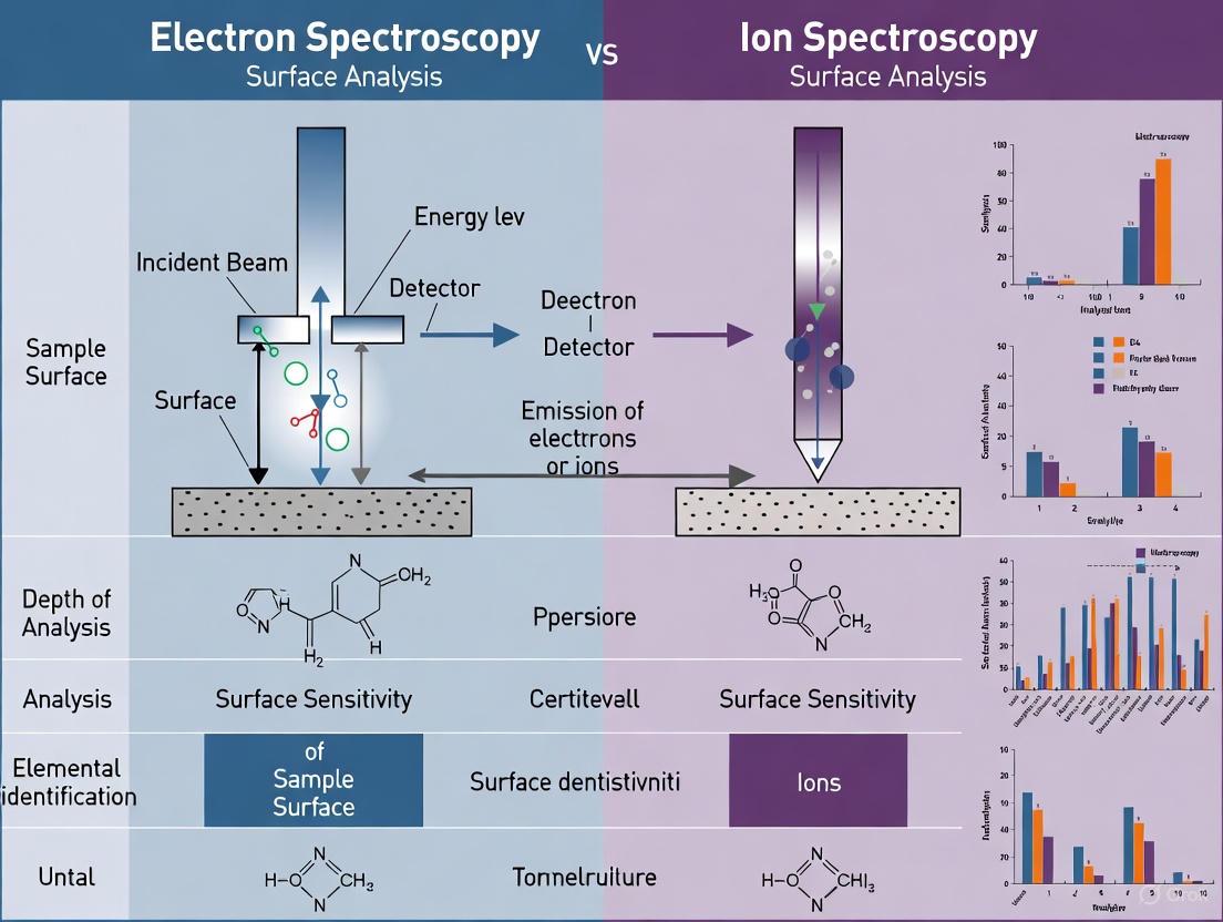
Surface analysis is a critical discipline in analytical science, providing insights into the outermost layers of materials where many chemical and physical processes originate. For researchers in fields ranging from drug development to nanotechnology, understanding the composition and chemistry of surfaces is essential. The techniques designed for this purpose primarily use either electron or ion probes to investigate surface characteristics. This guide provides an objective comparison of the major surface analysis techniques, with a specific focus on the divide between electron and ion spectroscopy methods. We will explore the fundamental principles, analytical capabilities, and practical applications of these techniques, supported by current experimental data and protocols to inform your research decisions.
The three most widely applied surface analysis techniques are X-ray Photoelectron Spectroscopy (XPS), Auger Electron Spectroscopy (AES), and Secondary Ion Mass Spectrometry (SIMS) [1]. XPS and AES fall under the category of electron spectroscopy, while SIMS represents ion spectroscopy. Each technique offers unique advantages and suffers from specific limitations, making them complementary rather than competitive for comprehensive surface characterization.
Fundamental Principles: Electron vs. Ion Spectroscopy
Electron Spectroscopy Techniques
Electron spectroscopy techniques utilize incident particles (X-rays or electrons) to eject electrons from the sample surface, which are then analyzed to determine surface composition and chemical state.
X-ray Photoelectron Spectroscopy (XPS), also known as Electron Spectroscopy for Chemical Analysis (ESCA), operates on the photoelectric effect. When a material is irradiated with X-rays, electrons are ejected from core levels. The kinetic energy of these photoelectrons is measured, allowing calculation of their binding energy, which is element-specific and sensitive to chemical environment [1]. XPS provides excellent quantitative information and chemical state identification, making it the most commonly used surface analysis technique [1].
Auger Electron Spectroscopy (AES) uses a focused electron beam to create core holes in atoms. The subsequent relaxation process leads to emission of Auger electrons, whose energies are characteristic of the elements present [1]. AES typically offers superior spatial resolution compared to XPS (can be below 10 nm) and can in some cases provide better chemical state information, particularly for carbon on metal surfaces [1].
Ion Spectroscopy Techniques
Ion spectroscopy techniques use energetic primary ions to sputter material from the sample surface, then analyze the ejected particles.
Secondary Ion Mass Spectrometry (SIMS) bombards the surface with primary ions (typically O₂⁺, Cs⁺, Ga⁺, or Bi₃⁺), causing the ejection (sputtering) of neutral atoms and molecules, as well as positively and negatively charged secondary ions. These secondary ions are then analyzed by mass spectrometry [1]. SIMS offers exceptional sensitivity (parts-per-billion to parts-per-million range), the ability to detect all elements including hydrogen and isotopes, and high spatial resolution imaging capabilities.
A variation of SIMS, sputtered neutral mass spectrometry (SNMS), measures the mass spectrum of the neutral species emitted, which are ionized after leaving the surface [1].
Table 1: Fundamental Characteristics of Major Surface Analysis Techniques
| Technique | Primary Probe | Detected Signal | Information Obtained | Vacuum Requirement |
|---|---|---|---|---|
| XPS | X-rays | Photoelectrons | Elemental composition, chemical state, oxidation state | Ultra-high vacuum (UHV) |
| AES | Electrons | Auger electrons | Elemental composition, chemical state (for some elements) | UHV |
| SIMS | Ions | Secondary ions | Elemental and isotopic composition, molecular structure, trace impurities | UHV |
Technical Comparison of Capabilities
Detection Capabilities and Limitations
Each surface analysis technique has distinct strengths and limitations in terms of what it can detect and quantify.
XPS does not directly detect hydrogen (H) or helium (He), though the effect of hydrogen on other elements can sometimes be observed indirectly [1]. It provides relatively straightforward quantification with detection limits typically around 0.1-1 at%. Modern XPS instruments achieve spatial resolution in the 1-10 μm range, with synchrotron-based systems reaching approximately 150 nm [1].
AES similarly cannot directly detect H or He [1]. Its major advantage lies in superior spatial resolution, as electron beams can be focused to small areas, enabling nanoscale analysis. AES detection limits are similar to XPS but with better spatial resolution for mapping applications.
SIMS excels in detection capabilities, able to identify all elements including hydrogen and distinguish between isotopes [1]. This isotopic discrimination is particularly useful when an oxygen beam is used for analysis, where oxygen from the surface can be distinguished from the oxygen in the beam [1]. SIMS offers exceptional sensitivity with detection limits in the parts-per-billion to parts-per-million range, though quantification is more challenging than for XPS.
Spectral Complexity and Interpretation
The complexity of data interpretation varies significantly between techniques.
XPS spectra are generally the simplest to interpret, with well-resolved peaks corresponding to specific elemental transitions and chemical states [1]. This relative simplicity contributes to its widespread use and makes quantification more straightforward.
AES spectra can be more complex due to the involvement of three energy levels in the Auger process, but still generally provide interpretable elemental and some chemical information.
SIMS produces the most complex spectra, as large molecular fragments from the material are formed in addition to elemental ions [1]. While this provides rich molecular information, it complicates interpretation and quantification. The complexity is particularly pronounced when analyzing organic materials or complex molecular structures.
Table 2: Analytical Performance Comparison of Surface Analysis Techniques
| Parameter | XPS | AES | SIMS |
|---|---|---|---|
| Elements Detected | All except H and He | All except H and He | All elements, including H and He |
| Detection Limit | 0.1-1 at% | 0.1-1 at% | ppb-ppm range |
| Spatial Resolution | 1-10 μm (150 nm with synchrotron) | <10 nm | 50-100 nm (with Ga⁺ LMIG) |
| Chemical Information | Excellent (oxidation states, functional groups) | Good for some elements | Molecular structure, fragments |
| Quantification | Excellent (relative accuracy 5-10%) | Good (relative accuracy 10-15%) | Difficult (requires standards) |
| Depth Resolution | 2-5 nm (angle-resolved) | 2-5 nm | 1-3 nm (static SIMS) |
| Isotopic Detection | No | No | Yes |
Recent Technological Advances
Instrumental Developments
Surface analysis techniques continue to evolve with significant improvements in capability and accessibility.
XPS has seen remarkable advancements, including Hard X-ray Photoelectron Spectroscopy (HAXPES), which uses higher energy X-rays (from silver, chromium, or gallium sources instead of conventional aluminum or magnesium sources) to probe deeper interfaces and reduce surface contamination effects [1]. Near Ambient Pressure XPS (NAP-XPS) represents another major advancement, allowing chemical analysis of surfaces in reactive environments rather than requiring ultra-high vacuum [1]. This enables studies of corrosion, microorganisms, and catalytic processes under more realistic conditions.
AES and SIMS instruments have achieved higher spatial resolutions through improved focusing of electron and ion beams [1]. While the number of manufacturers of commercial AES and SIMS instruments has decreased over recent decades, there remains healthy competition in the XPS instrument market, driving continued innovation [1].
Miniaturization and Specialized Applications
The field has witnessed significant progress in miniaturization, similar to trends in related analytical techniques. While not directly applied to XPS, AES, or SIMS in the search results, developments in Drift Tube Ion Mobility Spectrometry (DT-IMS) demonstrate the broader trend toward portability and field deployment through miniaturization, improved ion shutters, drift tubes, and integrated chip-based pre-separation methods [2].
In pharmaceutical and forensic applications, novel approaches like Extractive-Liquid Sampling Electron Ionization-Mass Spectrometry (E-LEI-MS) combine ambient sampling with the high identification power of electron ionization, enabling rapid analysis of drugs and contaminants with minimal sample preparation [3]. This technique has been successfully applied to detect active pharmaceutical ingredients and excipients in various drug formulations, as well as benzodiazepines in simulated forensic scenarios involving adulterated cocktails [3].
Experimental Protocols
Representative Workflow: Surface Analysis of Pharmaceutical Compounds
The following dot code provides a workflow for surface analysis of pharmaceutical compounds using E-LEI-MS, based on published methodologies [3]:
Figure 1: Workflow for surface analysis of pharmaceutical compounds using E-LEI-MS.
Detailed Methodologies
Protocol 1: Analysis of Active Pharmaceutical Ingredients (APIs) using E-LEI-MS [3]
- Sample Preparation: Twenty commercially available pharmaceuticals containing 16 different APIs were analyzed without any pre-treatment. Samples included tablets, lozenges, and gels.
- Instrument Configuration: E-LEI-MS system coupled to a triple quadrupole mass spectrometer equipped with an EI source. The system includes a solvent-release mechanism with a syringe pump and a sampling tip consisting of two coaxial tubes.
- Solvent Delivery: Acetonitrile was pumped through the outer tubing onto the sample surface at a controlled rate.
- Liquid Extraction: Analytes were directly extracted from the sample surface wetted by solvent droplets.
- Vacuum Aspiration: The liquid extract was immediately aspirated by the high vacuum of the EI source through the inner capillary.
- Vaporization and Ionization: The extract passed through a vaporization microchannel (VMC) heated to 300°C, then into the EI source where ionization occurred at 70 eV.
- Mass Analysis: Ions were analyzed by the triple quadrupole mass spectrometer in full scan mode (m/z 50-500).
- Data Analysis: Spectra were compared against commercial EI spectral libraries for compound identification.
Protocol 2: Analysis of Benzodiazepines in Fortified Cocktails (Simulating DFSA Scenarios) [3]
- Sample Preparation: Six benzodiazepines (clobazam, clonazepam, diazepam, flunitrazepam, lorazepam, and oxazepam) were used to fortify a gin tonic cocktail at concentrations of 20 mg/L and 100 mg/L.
- Spot Preparation: 20 μL of adulterated cocktails were spotted on a watch glass surface and analyzed as dried spots.
- Analysis Conditions: Similar to Protocol 1, but using high-resolution accurate-mass quadrupole time-of-flight (Q-ToF) mass spectrometry for confident compound identification.
- Identification Criteria: Accurate mass measurement with mass error < 5 ppm and isotopic pattern matching.
Essential Research Reagents and Materials
Table 3: Essential Research Reagents and Materials for Surface Analysis Experiments
| Item | Function | Application Example |
|---|---|---|
| Acetonitrile (HPLC grade) | Extraction solvent | Dissolving and extracting analytes from sample surfaces in E-LEI-MS [3] |
| Standard solutions | Calibration and quantification | Preparing reference standards for benzodiazepines at concentrations of 20, 100, and 1000 mg/L [3] |
| Silica capillaries | Liquid transport | Inner capillary (40-50 μm I.D.) for transporting liquid extract to MS [3] |
| Peek tubing | Solvent delivery | Outer tubing (450 μm I.D.) for delivering solvent to sample surface [3] |
| Vaporization microchannel (VMC) | Sample vaporization | Facilitating vaporization and transport of liquid extract into ion source [3] |
| Syringe pump | Solvent delivery control | Precisely controlling solvent flow rate (typically 1-10 μL/min) [3] |
| Manual microfluid valve | Flow control | Regulating liquid flow into the mass spectrometer [3] |
Comparative Performance in Practical Applications
Application-Specific Considerations
The choice of surface analysis technique depends heavily on the specific application requirements:
For chemical state analysis and quantitative composition, XPS is generally preferred due to its straightforward interpretation and reliable quantification [1]. Applications include surface contamination analysis, coating characterization, and failure analysis.
For high-spatial resolution elemental mapping, AES provides superior performance with its finely focused electron beam [1]. This makes it valuable for semiconductor device analysis, grain boundary studies, and microelectronic failure analysis.
For trace detection and molecular identification, SIMS offers unparalleled sensitivity and molecular information [1]. Applications include dopant profiling in semiconductors, organic contaminant identification, and biological surface characterization.
For atmospheric or semi-atmospheric pressure studies, NAP-XPS enables investigation of surfaces under realistic environmental conditions, unlike traditional UHV techniques [1]. This is particularly valuable for catalytic studies, corrosion science, and biological surface analysis.
Data Analysis Challenges and Solutions
Data interpretation remains a significant challenge across all surface analysis techniques, particularly for non-experts.
In XPS, peak fitting is one of the most commonly used procedures, yet approximately 40% of papers show incorrect fitting of peaks [1]. Common errors include using symmetrical peaks for asymmetrical metal peaks, not applying appropriate constraints for doublet relative intensities and separations, and incorrectly setting full-width at half-maximum (FWHM) parameters [1]. For example, the Ti 2p₁/₂ FWHM is typically about 20% larger than the FWHM of the Ti 2p₃/₂ peak, a detail often overlooked in improper peak fitting [1].
SIMS data interpretation is challenged by spectral complexity, with numerous peaks corresponding to molecular fragments in addition to elemental ions. Multivariate analysis techniques are often required for comprehensive data interpretation.
Software solutions continue to evolve, but fully automated analysis and interpretation remain problematic. Manufacturers' claims of completely automated analysis and reporting often fall short in practice, frequently generating reports with errors [1]. Organizations such as ISO continue to work on methods for improving data analysis standardization.
Surface analysis techniques provide indispensable tools for characterizing the outermost layers of materials, with XPS, AES, and SIMS representing the three most widely applied methods. Each technique offers unique capabilities: XPS excels in quantitative analysis and chemical state determination; AES provides superior spatial resolution for elemental mapping; while SIMS offers exceptional sensitivity and isotopic discrimination.
The choice between electron spectroscopy (XPS, AES) and ion spectroscopy (SIMS) depends on specific analytical requirements including detection sensitivity, spatial resolution, need for chemical state information, and whether isotopic or molecular information is required. Recent advancements such as HAXPES, NAP-XPS, and hybrid techniques like E-LEI-MS continue to expand application possibilities across pharmaceutical, forensic, materials, and biological research.
As these techniques evolve, challenges remain in data interpretation, particularly in peak fitting for XPS and spectral complexity in SIMS. Ongoing developments in instrumentation, data processing software, and standardization efforts promise to address these challenges, further enhancing the value of surface analysis across scientific disciplines.
Surface analysis is critical for understanding material properties in fields ranging from drug development to nanotechnology. Among the most prominent techniques are X-ray Photoelectron Spectroscopy (XPS) and Auger Electron Spectroscopy (AES), both belonging to the electron spectroscopy family. These techniques probe the topmost 1-10 nanometers of a material, providing invaluable information about elemental composition and chemical state [4] [5]. While they share the common principle of analyzing ejected electrons to characterize surfaces, their excitation mechanisms and the specific information they deliver differ significantly. This guide provides a detailed comparison of XPS and AES, outlining their fundamental mechanisms, experimental protocols, and appropriate applications within the broader context of surface science research.
The fundamental physical process for both techniques begins with the creation of a core-hole in an atom. Where they differ is in the initial excitation mechanism and the subsequent relaxation process that produces the detected electron. XPS relies on the photoelectric effect, where an incident X-ray photon is absorbed, directly ejecting a photoelectron. In contrast, AES uses a focusedelectron beam to create the initial core hole, and the detected signal comes from a secondary electron emitted during the relaxation process that follows [1]. This fundamental distinction in excitation and emission mechanisms dictates their relative strengths, weaknesses, and ideal application areas.
Fundamental Mechanisms and Theoretical Background
X-ray Photoelectron Spectroscopy (XPS) Mechanism
XPS, also known as Electron Spectroscopy for Chemical Analysis (ESCA), operates on the principle of the photoelectric effect. When a material is irradiated with X-rays of known energy, photons are absorbed by atoms, ejecting core-level electrons known as photoelectrons. The kinetic energy (KE) of these ejected photoelectrons is measured by the instrument, and the electron binding energy (BE) is calculated using the fundamental equation [6] [5]:
Binding Energy (BE) = Photon Energy (hν) – Kinetic Energy (KE) – Work Function (φ) [5]
The binding energy is a characteristic value for each element and electronic shell, enabling qualitative analysis. Furthermore, because the binding energy is sensitive to the chemical environment of the atom, XPS provides chemical state information. For example, the binding energy for carbon in a C-C bond is different from that in a C-O bond [4] [5]. The average depth of analysis for XPS is very shallow, typically less than 10 nm, making it exceptionally surface-sensitive [4]. Its detection limits are generally in the parts per thousand range, though parts per million (ppm) can be achieved with long collection times and surface concentration [5].
Auger Electron Spectroscopy (AES) Mechanism
The AES process is a three-step phenomenon initiated by a high-energy electron beam (typically 3-20 keV). First, the incident electron collides with an atom, ejecting a core-level electron and creating a core-hole. Second, an electron from a higher energy level fills this vacancy. Third, the energy released from this relaxation is transferred to another electron, which is then ejected from the atom; this ejected electron is called an Auger electron (named after Pierre Auger) [1]. The kinetic energy of the Auger electron is characteristic of the element from which it was emitted but is generally independent of the incident beam energy.
The kinetic energy of an Auger electron is determined by the energy levels of the three orbitals involved in the process (the initial core-hole, the filling electron, and the ejected electron). For a transition involving the K, L₁, and L₂₃ levels, the kinetic energy is approximately EKinetic ≈ EK – EL₁ – EL₂₃, where E denotes the binding energy of the respective levels [7]. Unlike XPS, the Auger process does not directly provide the same detailed chemical state information, though chemical shifts in Auger peaks can still occur and are sometimes used in specialized Auger parameter studies for additional chemical information.
Conceptual Workflow Diagram
The following diagram illustrates the core mechanisms and comparative workflows of XPS and AES analysis.
Figure 1: Comparative mechanisms and workflows of XPS and AES surface analysis techniques.
Comparative Technical Specifications
For researchers selecting the appropriate technique, a direct comparison of key technical parameters is essential. The following table summarizes the fundamental characteristics of XPS and AES.
Table 1: Technical comparison of XPS and AES
| Parameter | XPS (ESCA) | AES |
|---|---|---|
| Primary Excitation Source | X-ray photons (e.g., Al Kα, Mg Kα) [4] | High-energy electron beam (3-20 keV) [1] |
| Detected Particle | Photoelectrons [5] | Auger electrons [1] |
| Primary Information | Elemental identity, chemical state, and oxidation state [4] [5] | Elemental identity and lateral distribution [1] |
| Spatial Resolution | ~10 µm (lab source); can be < 150 nm with synchrotrons [1] | Higher than XPS; can be focused to nanometers [1] |
| Detection Limits | ~0.1-1.0 at% (1000 ppm); can reach ppm with long acquisition [5] | Similar to XPS, but highly dependent on element and matrix [7] |
| Quantitative Accuracy | Excellent (90-95% for major peaks) with relative sensitivity factors [5] | Good, but can be more complex than XPS due to background [7] |
| Chemical State Sensitivity | Excellent, a key strength of the technique [4] [5] | Moderate; chemical shifts are smaller and more complex to interpret [1] |
| Sample Damage | Generally low for most solids; can degrade some polymers [5] | Higher potential for damage due to focused electron beam [1] |
| Vacuum Requirement | High vacuum (HV) or ultra-high vacuum (UHV) [5] | Ultra-high vacuum (UHV) is essential [1] |
Experimental Protocols and Methodologies
Standard XPS Analysis Protocol
1. Sample Preparation: Samples must be solid and compatible with ultra-high vacuum (UHV ~10⁻⁹ mbar). Conducting samples can be mounted directly, while insulating samples may require charge neutralization with a low-energy electron flood gun. Sample size is variable, with modern instruments accepting samples from millimeters to several centimeters in size [5].
2. Instrument Calibration and Setup: The energy scale of the spectrometer is calibrated using standard reference samples like clean gold or copper foil. The analyst selects an appropriate X-ray source (typically monochromatic Al Kα at 1486.6 eV for high resolution), and the analyzer pass energy is set to achieve the desired balance between energy resolution and signal-to-noise ratio [7] [6].
3. Data Acquisition:
- Survey Scan: A wide energy range scan (e.g., 0-1100 eV binding energy) is first acquired to identify all elements present on the surface. Acquisition time is typically 1-20 minutes [5].
- High-Resolution Regional Scans: Narrow energy windows covering the core-level peaks of identified elements are scanned with higher energy resolution to determine chemical states. Acquisition times range from 1-15 minutes per region, and multiple sweeps are often used to improve the signal-to-noise ratio [5].
4. Data Processing and Quantification:
- Background Subtraction: A suitable algorithm (e.g., Shirley or Tougaard background) is applied to remove the inelastically scattered electron background [7] [8].
- Peak Fitting: High-resolution spectra are deconvoluted using curve-fitting with appropriate peak shapes (e.g., mixed Gaussian-Lorentzian functions) and constraints based on known chemical states and spin-orbit splitting [1] [6].
- Quantification: The area under each photoelectron peak is calculated and divided by an element-specific relative sensitivity factor (RSF) to determine atomic concentrations [7] [5]. The formula for the atomic concentration of element A is: at% A = (I_A / RSF_A) / Σ(I_n / RSF_n), where I is the measured peak area.
Standard AES Analysis Protocol
1. Sample Preparation: Similar to XPS, samples must be UHV-compatible. Due to the use of an electron beam, sample charging of insulators can be more challenging to manage than in XPS.
2. Instrument Setup: The electron gun is configured with a specific beam energy (e.g., 10 keV) and current. The electron optic column is aligned to achieve the smallest possible spot size for high-spatial-resolution analysis. The analyzer is set to a constant pass energy for consistent resolution [7].
3. Data Acquisition: AES data can be acquired in two primary modes:
- Direct Spectrum Mode (N(E) vs. E): This mode provides the true electron energy distribution and is required for accurate quantitative analysis. Peak areas are integrated after background removal [7].
- Differential Spectrum Mode (dN(E)/dE vs. E): This was the traditional, more rapid mode where the peak-to-peak height in the differentiated spectrum is used as a semi-quantitative measure of elemental concentration. However, this method is strongly influenced by chemical state changes and peak shape, making it less reliable for quantification than the direct spectrum method [7].
4. Data Processing and Quantification:
- For quantification from direct spectra, the background is carefully removed, often using methods like the Tougaard algorithm [7].
- The peak area for a specific Auger transition is measured. Quantitative analysis involves complex calculations or sensitivity factors that account for the ionization cross-section, backscattering factor, and inelastic mean free path. The total intensity from all transitions originating from an ionized shell often provides the best correlation with theory [7].
Depth Profiling Methodology
Both techniques can be used for depth profiling by combining analysis with sequential material removal via sputtering by an ion beam (e.g., Ar⁺) [9] [8].
1. Protocol: A cycle consists of (1) acquiring spectra from the fresh surface, (2) etching the surface for a fixed time using a rastered ion beam, and (3) repeating until the desired depth is reached [9].
2. Optimization Considerations:
- Ion Beam Parameters: Lower ion energies and larger primary ion species (e.g., Xe⁺) improve depth resolution by reducing atomic mixing [9].
- Incidence Angle: Shallow (grazing) angles improve depth resolution by reducing the ion penetration depth [9].
- Crater Quality: The sputtered crater must be large and flat, with the analysis area well-centered to avoid crater wall effects [9].
- Sample Rotation: Azimuthal rotation during sputtering significantly reduces induced roughness, leading to higher resolution profiles, especially for polycrystalline materials [9].
Table 2: Key reagents and materials for electron spectroscopy
| Item | Function |
|---|---|
| Monochromatic Al Kα X-ray Source | Standard laboratory X-ray source for XPS (1486.6 eV); provides narrow linewidth for high-resolution chemical state analysis [6] [5]. |
| High-Energy Electron Gun | Source of primary electrons for AES excitation; can be focused to a fine probe for high-spatial-resolution mapping [1]. |
| Argon Gas Cluster Ion Source | Advanced sputtering source for depth profiling organic and polymeric materials; minimizes damage compared to monatomic ions [8] [10]. |
| Charge Neutralization Flood Gun | Source of low-energy electrons and ions to compensate for surface charging on insulating samples during analysis, essential for accurate data [9] [5]. |
| Certified Standard Reference Samples | Samples with known composition (e.g., Au, Cu, Si) for quantitative calibration of the spectrometer's intensity/energy response function [7]. |
| High-Purity Sputter Gases (Ar, Xe) | Inert gases for ion guns used in sample cleaning and depth profiling; high purity is critical to avoid surface contamination [9]. |
Data Interpretation and Analysis
Quantitative Analysis and Sensitivity Factors
The foundation of quantification in both XPS and AES is the scaling of measured peak intensities with element-specific relative sensitivity factors (RSFs). In XPS, the process is relatively straightforward: the integrated area of a photoelectron peak is divided by its RSF, and the results are normalized to 100% to obtain atomic percentages [5]. These RSFs account for the photoionization cross-section (typically from Scofield's calculations) and the energy-dependent transmission of the electron analyzer [7].
Quantification in AES is inherently more complex. The Auger current depends not only on the ionization cross-section but also on the backscattering factor (the contribution of incident electrons that are backscattered and cause additional ionizations) and complex core-hole relaxation dynamics, including Coster-Kronig transitions [7]. Studies show that the best quantitative correlations are achieved by considering the total intensity for all Auger transitions originating from an ionized shell, using the Casnati et al. ionization cross-section and specific inelastic mean free path calculations [7].
Spectral Features and Chemical State Information
XPS: Chemical state identification is a principal strength. A shift in the binding energy of a photoelectron peak indicates a change in the chemical environment of the atom. For example, the Si 2p peak will have a distinct, higher binding energy in SiO₂ compared to pure Si. Peak fitting of high-resolution spectra is used to deconvolve these different chemical states [1] [6]. A common challenge, however, is that in about 40% of published papers, peak fitting is performed incorrectly, for instance, by using symmetrical peaks for inherently asymmetrical metallic peaks or misapplying constraints on doublet separations and intensities [1].
AES: While the primary Auger peak energy is used for elemental identification, the Auger line shape can also be sensitive to chemical environment. For instance, the carbon KLL spectrum is markedly different between graphite, carbide, and hydrocarbon states. However, interpreting these shape changes is often less intuitive than interpreting XPS chemical shifts [1].
Current Trends and Advancements
The field of electron spectroscopy is continuously evolving. Key trends shaping its future include:
- Democratization and Automation: Instrumentation is becoming more user-friendly and automated, extending access beyond specialist operators. Intelligent software is being developed to improve data reproducibility and integrity, though fully automated interpretation remains a challenge [1] [10].
- Advanced Light Sources: The use of Hard X-ray Photoelectron Spectroscopy (HAXPES) with laboratory Cr or Ga sources or synchrotrons allows probing of deeper bulk regions and interfaces (tens of nanometers), reducing surface sensitivity issues [1] [6].
- Near-Ambient Pressure XPS (NAP-XPS): This advancement enables the study of surfaces in the presence of gases or vapors, opening new frontiers in catalysis, environmental science, and electrochemistry [1].
- Improved Sputtering: The development of gas cluster ion beams (e.g., Arₙ⁺, n>1000) has revolutionized depth profiling of organic materials, polymers, and pharmaceuticals by significantly reducing the ion beam damage associated with traditional monatomic ions [9] [8] [10].
XPS and AES are powerful, complementary techniques in the surface scientist's toolkit. The choice between them depends heavily on the specific analytical question.
- Choose XPS when the primary requirements are excellent chemical state information, straightforward quantitative analysis of homogeneous surfaces, and minimal risk of beam-induced damage for sensitive materials. It is the more universally applied technique for general surface chemical characterization.
- Choose AES when the analysis demands very high lateral spatial resolution (down to the nanometer scale) for mapping elemental distributions on the micro- to nano-scale, and when the sample is conductive and robust enough to withstand electron beam exposure.
Within the broader thesis comparing electron and ion spectroscopy techniques, this guide establishes that electron-based spectroscopies like XPS and AES excel in providing direct information on elemental composition and chemical bonding from the outermost surface layers. Their integration with ion beam sputtering for depth profiling creates a powerful, hybrid approach for three-dimensional material characterization, bridging the information gap between pure electron and pure ion spectroscopy methods.
Surface compositional analysis is critical in fields ranging from materials science to pharmaceutical development, where understanding the outermost layers of a material is essential for predicting its performance and stability. Ion spectroscopy techniques, particularly Secondary Ion Mass Spectrometry (SIMS) and Sputtered Neutral Mass Spectrometry (SNMS), represent two powerful approaches for obtaining detailed chemical information from surfaces. These techniques operate on the principle of surface erosion by ion beam sputtering but differ fundamentally in the species they detect and their resulting analytical capabilities. Within the broader context of surface analysis techniques, which include electron spectroscopies like XPS and AES, SIMS and SNMS offer unique advantages for elemental and molecular characterization with excellent depth resolution and sensitivity. This guide provides a comprehensive comparison of SIMS and SNMS methodologies, presenting their fundamental mechanisms, comparative performance data, and practical experimental considerations to assist researchers in selecting the appropriate technique for their specific analytical challenges.
Fundamental Principles and Mechanisms
Secondary Ion Mass Spectrometry (SIMS)
The SIMS technique operates through a focused primary ion beam (typically Cs+, O2+, or Ga+) that bombards the sample surface, causing the ejection (sputtering) of atoms and molecules from the uppermost layers. A critical fraction of these sputtered particles become ionized (forming secondary ions) and are subsequently extracted into a mass analyzer for identification. The process involves multiple sequential steps: primary ion impact, energy transfer through collision cascades, sputtering of material, ionization of a fraction of the sputtered particles, and finally mass analysis of the secondary ions. The detected secondary ion intensities provide information about the elemental, isotopic, and molecular composition of the analyzed surface volume.
SIMS is particularly renowned for its exceptional sensitivity, capable of detecting elements present at trace levels (parts-per-billion to parts-per-million range). However, this sensitivity comes with a significant analytical challenge known as the matrix effect, where the ionization probability of sputtered particles—and thus the measured signal intensity—depends strongly on the chemical environment of the element within the sample. This effect complicates quantitative analysis as relative sensitivity factors can vary by orders of magnitude between different matrices, requiring careful calibration with matrix-matched standards for accurate quantification [11].
Sputtered Neutral Mass Spectrometry (SNMS)
SNMS was developed to overcome the matrix effects that plague quantitative analysis in SIMS. While the initial sputtering process in SNMS is similar to SIMS, the fundamental difference lies in the detection scheme. In SNMS, the majority sputtered neutral atoms and molecules (which constitute over 99% of the total sputtered flux) are selectively ionized after leaving the sample surface using a dedicated post-ionization mechanism. This physical separation of the sputtering and ionization processes effectively decouples the emission and ionization events, dramatically reducing matrix dependence [12] [13].
Various post-ionization methods have been implemented in SNMS instruments. The electron gas SNMS approach utilizes a dense, confined electron gas maintained at low pressures (∼10⁻³ Pa) through which the sputtered neutrals pass and undergo electron impact ionization. Alternative implementations employ electron beams or high-power lasers for post-ionization. The use of Cs+ primary ions in SNMS has been shown to improve depth resolution compared to Ar+ bombardment without altering the relative sensitivity factors used for quantification, making it advantageous for depth profiling of layered structures [12]. Additionally, SNMS spectra are notably cleaner than SIMS spectra as they contain "no significant amount of molecules," reducing spectral interferences [12].
Comparative Performance Analysis
Technical Comparison of SIMS and SNMS
Table 1: Fundamental characteristics and comparative performance of SIMS and SNMS
| Parameter | SIMS | SNMS |
|---|---|---|
| Detected Species | Secondary ions | Post-ionized sputtered neutrals |
| Ionization Process | Occurs during sputtering | Post-ionization after sputtering |
| Matrix Effects | Strong (major limitation) | Minimal (key advantage) |
| Useful Yield | ~0.1-10% (varies greatly with matrix) | Can approach >50% for electron gas SNMS |
| Quantification | Requires matrix-matched standards | Direct quantification with relative sensitivity factors |
| Molecular Information | Yes (detects molecular ions) | Limited (primarily atomic species) |
| Detection Limits | Excellent (ppb-ppm range) | Good (ppm range typically) |
| Depth Resolution | Good, but can be degraded by atomic mixing | Superior, improved with Cs+ primary ions and sample biasing [12] |
| Dynamic Range | Good | High (improved in combined instruments) [13] |
Quantitative Analysis Capabilities
The comparative studies between MCs+-SIMS and electron-beam SNMS reveal critical differences in their quantitative capabilities. In SNMS, the relative sensitivity factors (RSFs) show minimal matrix dependence, enabling more straightforward quantification of heterostructure depth profiles. In contrast, MCs+-SIMS demonstrates matrix-dependent RSFs that complicate quantitative analysis, despite its improved depth resolution compared to conventional SIMS modes [12]. The fundamental reason for this difference lies in the ionization mechanism: since SNMS detects neutrals that are ionized in a controlled environment after sputtering, the ionization probability becomes largely independent of the sample matrix.
For depth profiling applications, SNMS offers advantages in depth resolution through technical implementations such as biasing the sample against the primary ion beam, which reduces the net energy of primary ions and creates a more grazing impact angle [12]. Combined SNMS/SIMS instruments have been developed to leverage the strengths of both techniques, providing high dynamic range and improved detection limits for comprehensive trace and depth profile analysis [13].
Experimental Protocols and Methodologies
SIMS Experimental Protocol for Surface Analysis
Instrument Setup and Parameters: Time-of-Flight (ToF) SIMS instruments are widely used for surface analysis due to their high mass resolution and sensitivity. The experimental protocol begins with sample preparation, which typically involves mounting the specimen on a conductive substrate to mitigate charging effects during analysis. For insulating samples, electron flood guns are employed for charge compensation. The primary ion source (commonly liquid metal ion guns like Ga+ or Bi3+ for high spatial resolution, or Cs+ for enhanced negative secondary ion yield) is tuned to optimal parameters, with typical primary ion energies ranging from 10-30 keV. The mass spectrometer is mass-calibrated using known reference peaks prior to analysis [14] [15].
Data Acquisition and Analysis: Surface spectra are acquired in static SIMS mode using a low primary ion dose (<10¹³ ions/cm²) to ensure the analysis remains surface-specific. For depth profiling, dynamic SIMS employs higher primary ion doses with continuous sputtering to progressively reveal subsurface information. The secondary ions are extracted into the time-of-flight analyzer, separated by their mass-to-charge ratios, and detected using microchannel plate detectors. Data interpretation involves identifying elemental and molecular peaks through exact mass assignment, often supplemented by multivariate analysis techniques for complex organic and biological samples [14].
SNMS Experimental Protocol for Quantitative Depth Profiling
Instrument Configuration: SNMS instrumentation incorporates additional components compared to SIMS, primarily the post-ionization source situated between the sample and mass analyzer. In electron gas SNMS systems, a confined electron gas is maintained in a Wien filter configuration, where the sputtered neutrals pass through and undergo electron impact ionization. The electron beam SNMS variant employs a focused electron beam directed across the path of the sputtered neutral flux. Primary ion sources for SNMS commonly use Cs+ ions, which have been shown to improve depth resolution without affecting quantification relative to Ar+ bombardment [12] [13].
Measurement Procedure: Samples are typically mounted on conducting holders with the surface normal aligned at a specific angle (often 45°) relative to both the primary ion gun and the extraction optics. The post-ionization source parameters (electron energy and density for electron gas SNMS) are optimized to maximize ionization efficiency while minimizing energy broadening of the detected ions. During depth profiling, the primary ion beam is rastered over the analysis area while continuously sputtering the sample. The detected ion signals are recorded as a function of sputtering time, which is subsequently converted to depth scale using pre-calibrated sputter rates for the specific material system. Quantitative composition is determined using relative sensitivity factors derived from standard reference materials [12] [13].
Cryogenic Sample Preparation for Nanomedicine Characterization
Advanced applications in pharmaceutical nanomedicine characterization require specialized sample preparation protocols. For analyzing temperature-sensitive materials like PEGylated liposomal nanomedicines, a cryogenic protocol has been developed for ToF-SIMS analysis. This methodology involves rapid freezing of the nanoparticle suspension in liquid nitrogen slush to preserve the native structure and surface organization of the nanoparticles. The frozen hydrate sample is then transferred under vacuum to the SIMS analysis chamber using a specialized cryo-transfer system, maintaining temperatures below -120°C throughout the process. This approach prevents dehydration-induced reorganization of surface functional groups and enables accurate characterization of critical quality attributes such as PEG coating density on liposomal surfaces [14].
Research Reagent Solutions and Essential Materials
Table 2: Key research reagents and materials for SIMS and SNMS experiments
| Item | Function/Application | Technical Specifications |
|---|---|---|
| Primary Ion Sources | Sputtering and particle ejection from sample surface | Cs+, O2+, Ga+, Bi3+ liquid metal ion guns; Energy range: 0.5-30 keV |
| Conductive Substrates | Sample mounting and charge dissipation | Silicon wafers, indium foil, gold-coated substrates |
| Charge Compensation Systems | Neutralizing surface charge on insulating samples | Low-energy electron flood guns, pulsed electron sources |
| Cryogenic Transfer Systems | Preserving native structure of biological/soft materials | Liquid nitrogen slush, vacuum transfer stages, temperature control <-120°C |
| Standard Reference Materials | Quantification calibration and instrument performance verification | Certified ion implant standards, homogeneous alloy standards, organic thin films |
| Mass Resolution Calibrants | Mass scale calibration and resolution verification | Known molecular ions (e.g., CH3+, C2H5+, C3H7+ for low mass range) |
| Ultra-high Vacuum Components | Maintaining required operational pressure | Ion pumps, turbomolecular pumps, pressure < 10⁻⁸ Pa |
Application Scenarios and Technique Selection
Pharmaceutical and Nanomedicine Development
In pharmaceutical development, particularly for nanomedicine formulations like PEGylated liposomes, SIMS has emerged as a powerful characterization tool. The cryo-ToF-SIMS methodology enables precise characterization of critical quality attributes such as PEG coating density on liposomal surfaces, which directly influences biological stability and pharmacokinetics. This application demonstrates how SIMS can distinguish between liposome formulations with varying PEG-lipid contents (3.0 to 15.5 mol%) in their outer membranes, providing essential quality control for drug manufacturing processes. The ability to probe surface functionality densities without resorting to large-scale facilities like neutron beamlines makes SIMS particularly valuable for pharmaceutical R&D and regulatory studies [14].
Materials Science and Semiconductor Applications
Both SIMS and SNMS find extensive applications in materials science, particularly for semiconductor device characterization and thin film analysis. SIMS dominates applications requiring high sensitivity for dopant profiling and contaminant detection at trace levels, leveraging its exceptional detection limits for most elements. The magnetic sector and time-of-flight SIMS instruments are widely employed for these applications, with the time-of-flight segment accounting for a significant market share [15]. SNMS excels in applications demanding precise quantitative depth profiling of multilayer structures and thin film interfaces where matrix effects would compromise SIMS quantification. The combined SNMS/SIMS instruments are particularly valuable for comprehensive analysis requiring both high sensitivity and accurate quantification across multiple elements [13].
Technique Selection Guidelines
Selecting between SIMS and SNMS depends primarily on the specific analytical requirements:
Choose SIMS when: Ultimate detection sensitivity (ppb-ppm) is required; molecular or chemical state information is needed; analysis of insulating materials without conducting coatings; or when mapping trace element distributions with high spatial resolution.
Choose SNMS when: Accurate quantification without matrix-matched standards is essential; analyzing complex multilayer structures with changing matrix composition; primarily interested in atomic composition rather than molecular information; or when high useful yield and dynamic range are prioritized.
Consider combined approaches when: Both extreme sensitivity and accurate quantification are needed across different elements; analyzing unknown samples with potentially varying matrix effects; or when comprehensive characterization justifies the instrumental complexity.
SIMS and SNMS represent complementary approaches in the ion spectroscopy toolkit for surface compositional analysis. While SIMS offers superior sensitivity and molecular detection capabilities, SNMS provides more reliable quantification with minimal matrix effects. The continuing development of both techniques, including cryogenic preparation methods for biological samples and combined instrument platforms, expands their applicability across diverse fields from semiconductor technology to pharmaceutical development. Understanding their fundamental mechanisms, performance characteristics, and implementation requirements enables researchers to strategically deploy these powerful surface analysis techniques to address specific analytical challenges in both fundamental research and industrial applications.
Electron Kinetic Energies vs. Ion Mass-to-Charge Ratios
In the realm of analytical spectroscopy, two fundamental measured outputs form the cornerstone of a wide array of surface analysis and material characterization techniques: electron kinetic energies and ion mass-to-charge ratios. These measurements provide distinct yet complementary windows into the composition, structure, and properties of materials at the molecular and atomic levels. Techniques measuring electron kinetic energies, such as X-ray Photoelectron Spectroscopy (XPS) and Auger Electron Spectroscopy (AES), probe the electronic structure and chemical state of surface atoms. In contrast, techniques measuring ion mass-to-charge ratios, including various forms of Mass Spectrometry (MS) and Secondary Ion Mass Spectrometry (SIMS), provide information about elemental composition, molecular structure, and isotopic distribution. This guide provides an objective comparison of these fundamental approaches, their operating principles, applications, and performance characteristics within the context of surface science research, particularly for researchers and professionals in drug development and pharmaceutical sciences.
Fundamental Principles and Theoretical Background
Techniques Measuring Electron Kinetic Energies
Techniques based on measuring electron kinetic energies derive their analytical power from the photoelectric effect and related electron emission phenomena. When materials absorb photons or electrons with sufficient energy, they emit electrons whose kinetic energies carry specific information about their atomic and chemical origins.
X-ray Photoelectron Spectroscopy (XPS) operates by irradiating a sample with X-rays, causing the emission of photoelectrons from core electron orbitals. The kinetic energy (EK) of these photoelectrons is measured and related to their binding energy (EB) through the fundamental equation: [ EB = h\nu - EK - \Phi ] where ( h\nu ) is the energy of the incident X-ray photon and ( \Phi ) is the work function of the spectrometer [5]. This binding energy serves as a unique fingerprint for elemental identification and provides chemical state information, as the precise binding energy shifts slightly depending on the chemical environment of the atom.
Auger Electron Spectroscopy (AES) employs a different mechanism involving a three-step process. First, a high-energy electron beam creates a core-level vacancy. Second, an electron from a higher energy level fills this vacancy. Third, the energy released from this transition causes the emission of another electron—the Auger electron—whose kinetic energy is characteristic of the element and largely independent of the incident beam energy [16]. For AES, the kinetic energy of the Auger electron is typically described by: [ E{KL1L2} = EK - E{L1} - E{L2} ] where ( EK ), ( E{L1} ), and ( E{L_2} ) are the binding energies of electrons in the K, L₁, and L₂ shells, respectively [16].
Techniques Measuring Ion Mass-to-Charge Ratios
Techniques measuring ion mass-to-charge ratios (m/z) separate ions based on their motion in electromagnetic fields. The fundamental relationship governing these techniques stems from Newton's second law applied to charged particles in these fields.
In Mass Spectrometry (MS), the mass-to-charge ratio forms the primary measured parameter [17]. The basic principle involves converting sample molecules into gas-phase ions, separating them based on their m/z ratios, and detecting them quantitatively. Different mass analyzers achieve separation through different physical principles:
Time-of-Flight (TOF) analyzers separate ions based on the time they take to travel a fixed distance after being accelerated by a fixed electrical potential, following the relationship: [ t = L \times \sqrt{\frac{m/z}{2eV}} ] where ( t ) is the flight time, ( L ) is the flight path length, ( m/z ) is the mass-to-charge ratio, ( e ) is the elementary charge, and ( V ) is the acceleration voltage [18].
Dynamic Secondary Ion Mass Spectrometry (SIMS) uses a focused primary ion beam to sputter material from the sample surface, with a fraction of the sputtered material being ionized (secondary ions). These secondary ions are then extracted into a mass spectrometer (typically a double-focusing mass spectrometer using electrostatic and magnetic fields) that separates them according to their mass-to-charge ratio [19].
Technical Comparison and Performance Metrics
The following tables provide a detailed comparison of the key performance metrics and characteristics for representative techniques from both categories.
Table 1: Comparison of Key Performance Metrics for Surface Analysis Techniques
| Parameter | XPS | AES | Dynamic SIMS | TOF-MS |
|---|---|---|---|---|
| Primary Measured Output | Electron Kinetic Energy | Electron Kinetic Energy | Ion Mass-to-Charge Ratio | Ion Mass-to-Charge Ratio |
| Information Obtained | Elemental identity, chemical state, electronic structure | Elemental identity, chemical state (limited) | Elemental/isotopic composition, trace impurities | Molecular mass, structural information |
| Detection Limits | 0.1-1 at% (1000 ppm) [5] | ~1 at% | ppm to ppb range [19] | Variable (depends on ionization) |
| Depth Resolution | 5-10 nm [5] | <5 nm [20] | <10 nm [19] | Not surface-specific |
| Lateral Resolution | 10-200 μm [5] | ~8 nm [20] | Raster scanning or direct imaging capability [19] | Not surface-specific |
| Quantitative Accuracy | Excellent (90-95% for major elements) [5] | Good with standards | Quantitative with standards [19] | Good with internal standards |
Table 2: Applications and Limitations in Pharmaceutical Research Context
| Aspect | Electron Kinetic Energy Techniques | Ion Mass-to-Charge Ratio Techniques |
|---|---|---|
| Primary Strengths | Surface-sensitive, chemical state information, quantitative without standards, minimal damage (XPS) | Extreme sensitivity, isotopic discrimination, depth profiling, molecular identification |
| Common Pharmaceutical Applications | Surface composition of drug formulations, coating analysis, impurity identification | Drug metabolite identification, trace impurity analysis, protein characterization, drug delivery system studies |
| Sample Requirements | Solid surfaces, vacuum compatible, limited to ~1 cm size typically | Varied (solid, liquid, gas), specific preparation for different MS modes |
| Key Limitations | Limited sensitivity (ppm range), cannot detect H or He (XPS), potential sample damage | Destructive (SIMS), complex spectra for mixtures, matrix effects, requires calibration |
Experimental Protocols and Methodologies
Standard Experimental Workflow for Electron Kinetic Energy Techniques
The following diagram illustrates the generalized experimental workflow for techniques measuring electron kinetic energies, such as XPS and AES:
Sample Preparation Protocol for XPS/AES:
- Sample Cleaning: Remove surface contaminants using appropriate solvents (e.g., high-purity ethanol, acetone) or mild plasma cleaning
- Mounting: Secure sample on appropriate holder using conductive tape or clips to minimize charging
- Charge Neutralization: For insulating samples, apply low-energy electron flood gun for charge compensation (XPS)
- Surface Preservation: Maintain ultra-high vacuum conditions (10⁻⁷ to 10⁻⁹ Pa) to prevent surface contamination [5]
Data Collection Parameters for XPS:
- X-ray Source: Typically Al Kα (1486.7 eV) or Mg Kα (1253.7 eV)
- Analysis Area: 10 μm to 1 mm diameter, depending on instrument capabilities
- Pass Energy: 20-160 eV for survey scans, 10-50 eV for high-resolution regions
- Step Size: 1.0 eV for survey, 0.05-0.1 eV for high-resolution scans
- Acquisition Time: 2-5 minutes for survey, 5-20 minutes per high-resolution region [5]
Standard Experimental Workflow for Ion Mass-to-Charge Techniques
The following diagram illustrates the generalized experimental workflow for techniques measuring ion mass-to-charge ratios, such as Dynamic SIMS and TOF-MS:
Dynamic SIMS Depth Profiling Protocol:
- Primary Ion Source Selection: Choose between oxygen (Cs⁺) for electropositive elements or cesium (O₂⁺) for electronegative elements to enhance ionization yields [19]
- Sputtering Conditions: Optimize primary ion energy (typically 1-15 keV) and current to balance depth resolution and detection sensitivity
- Analysis Area Definition: Use electronic gating or physical apertures to select analysis area and exclude crater edge effects
- Data Acquisition: Continuously monitor secondary ion signals as function of sputtering time, converting to depth using calibrated sputtering rates
- Quantification: Apply relative sensitivity factors (RSFs) derived from matrix-matched standards to convert ion intensities to concentrations [19]
Mass Spectrometry Parameters for Drug Analysis:
- Ionization Method: Electrospray ionization (ESI) for polar compounds, atmospheric pressure chemical ionization (APCI) for low-to-medium polarity compounds [21]
- Mass Analyzer: Selection based on required resolution and application (Q-TOF for accurate mass, Orbitrap for high resolution)
- LC-MS Conditions: Reverse-phase C18 columns, water/acetonitrile gradients with 0.1% formic acid modifier
- Calibration: External calibration or internal standardization with stable isotope-labeled analogs [21]
The Scientist's Toolkit: Essential Research Reagents and Materials
Table 3: Key Research Reagents and Materials for Electron and Ion Spectroscopy
| Category | Specific Items | Function/Application |
|---|---|---|
| Reference Materials | Certified XPS reference samples (Au, Ag, Cu), ISO 15472 CRM | Energy scale calibration, instrument performance verification |
| Sample Preparation | Conductive tapes (Cu, C), sample holders, ultrasonic cleaner, plasma cleaner | Sample mounting, surface cleaning, charge reduction |
| Ion Source Materials | Cesium, oxygen, gallium primary ion sources | Primary ion beams for SIMS analysis [19] |
| MS Standards | Tuning and calibration solutions (e.g., NaI, CsI), PEG standards | Mass accuracy calibration, instrument performance verification |
| Chromatography | HPLC-grade solvents (water, acetonitrile, methanol), volatile buffers (ammonium acetate, formate) | Mobile phases for LC-MS applications [21] |
Applications in Drug Development and Pharmaceutical Research
Electron Spectroscopy Applications
XPS finds important applications in pharmaceutical research for characterizing the surface composition of drug formulations and delivery systems. The technique provides quantitative information about elemental composition and chemical states at the surface of solid dosage forms, which is critical for understanding coating uniformity, contamination, and surface segregation of excipients. For example, XPS can detect the presence of surface lubricants (e.g., magnesium stearate) on tablets, analyze the composition of multi-layer coatings, and identify surface contaminants that may affect drug performance or stability [5].
AES, with its superior lateral resolution, is particularly valuable for investigating small-scale surface features and inclusions in drug formulations. The technique can map the distribution of elements across tablet surfaces with sub-micrometer resolution, providing insights into mixing homogeneity and potential segregation of active pharmaceutical ingredients (APIs) or excipients during processing [20].
Mass Spectrometry Applications
Mass spectrometry techniques, particularly those measuring ion mass-to-charge ratios, play indispensable roles throughout drug discovery and development. During early discovery, MS is used for high-throughput characterization of synthetic compounds, confirmation of chemical structures, and purity assessment [21]. Liquid chromatography-mass spectrometry (LC-MS) becomes the workhorse technique for metabolite identification, pharmacokinetic studies, and impurity profiling during preclinical and clinical development.
Dynamic SIMS offers unique capabilities for elemental and isotopic imaging in pharmaceutical research. The technique can generate three-dimensional maps of elemental distributions within drug delivery systems with excellent sensitivity (ppm to ppb) and spatial resolution (down to nanometers). This is particularly valuable for studying the distribution of APIs and excipients in controlled-release formulations, investigating cross-layer diffusion in multi-layer tablets, and analyzing the incorporation of trace elements in drug crystals [19].
Charge Detection Mass Spectrometry (CD-MS) and Orbitrap Individual Ion Mass Spectrometry (I²MS) represent recent advances for analyzing heterogeneous and high-mass samples that challenge conventional MS approaches. These single-ion MS methods determine the mass of each individual ion from simultaneous measurement of both m/z and charge, enabling accurate mass measurements for samples ranging from kilo-Daltons to giga-Daltons. This capability opens new possibilities for characterizing viruses, gene therapies, vaccines, and other large biological assemblies relevant to modern pharmaceutical development [22].
Emerging Trends and Future Directions
The convergence of techniques measuring electron kinetic energies and ion mass-to-charge ratios represents an important trend in analytical science. Hybrid approaches that combine multiple spectroscopic techniques within a single instrument platform are becoming increasingly common, providing complementary data from the same sample region. For instance, combined XPS-SIMS instruments offer simultaneous elemental/chemical state information from XPS with high-sensitivity elemental and molecular information from SIMS.
Another significant development is the advancement of ambient pressure XPS, which enables analysis of samples under more realistic environmental conditions rather than requiring ultra-high vacuum. This capability is particularly relevant for pharmaceutical applications where hydrated states or atmospheric exposure conditions need to be preserved during analysis [5].
In the mass spectrometry domain, continued improvements in mass resolution, detection sensitivity, and data acquisition speeds are expanding the application space for pharmaceutical analysis. The development of higher-resolution CD-MS instruments promises to enable direct analysis of highly complex mixtures such as cell lysates and to facilitate studies of small ligand binding to large biological assemblies, including drug molecule interactions with viruses and other therapeutic targets [22].
Inherent Strengths and Fundamental Limitations of Each Approach
Surface analysis is a critical component of materials science, playing a pivotal role in characterizing material properties, investigating failure mechanisms, and driving innovation in fields ranging from semiconductor manufacturing to pharmaceutical development. These techniques enable researchers to determine the elemental composition, chemical state, and structure of the outermost layers of a material, which often dictate its performance and interaction with the environment. Among the diverse array of analytical methods available, electron and ion spectroscopy represent two foundational approaches that operate on different physical principles and offer complementary information.
This guide provides a comprehensive comparison of two prominent surface analysis techniques: Auger Electron Spectroscopy (AES) as a representative electron spectroscopy method, and Ion Scattering Spectroscopy (ISS) as a representative ion spectroscopy technique. We will objectively examine their fundamental principles, inherent strengths, limitations, and appropriate applications through structured data presentation, experimental protocols, and visualization tools to assist researchers in selecting the optimal technique for their specific analytical challenges.
Fundamental Principles and Instrumentation
Auger Electron Spectroscopy (AES)
AES is a surface-sensitive analytical technique that utilizes a high-energy electron beam (typically 2-10 kV) as an excitation source. When this electron beam strikes a sample surface, it ejects core-level electrons from atoms, creating excited ions. These ions relax through a radiative or non-radiative process. In the Auger process, an electron from a higher energy level fills the core hole, and the excess energy causes the emission of a third electron—the Auger electron. The kinetic energy of these emitted Auger electrons is characteristic of elements within the top 3-10 nm of the sample surface, providing elemental identification and compositional data [23] [24] [25].
Modern AES instruments incorporate several key components: an electron gun (often with field emission sources enabling spatial resolution down to <10 nm), an energy analyzer for detecting ejected electrons, an ion sputter gun for depth profiling, and an ultra-high vacuum chamber to prevent surface contamination and allow mean-free path for electrons. The ability to focus the electron beam to diameters of 10-20 nm makes AES exceptionally powerful for elemental analysis of small surface features [26] [27] [25].
Ion Scattering Spectroscopy (ISS)
ISS is an analytical technique that provides direct structural, topographical, and atomic compositional information at interfaces using ions as projectiles. In ISS, a beam of noble gas ions (typically He+, Ne+, or Ar+) with known energy is directed at the sample surface. When these primary ions collide with surface atoms, they lose energy through elastic binary collisions. The energy of the scattered ions is measured at a specific angle, and this energy loss is characteristic of the mass of the target atoms, following classical scattering laws [28].
The technique is particularly surface-sensitive, with information coming primarily from the outermost atomic layer. A variant called Neutral Impact Collision Ion Scattering Spectroscopy (NICISS) is especially useful for probing liquid interfaces. ISS achieves exceptional depth resolution of approximately 1-2 Å, depending on experimental parameters, making it ideal for studying atomic layer composition and structure [28].
Comparative Analysis of Techniques
Technical Capabilities and Performance Parameters
Table 1: Comparison of Key Technical Parameters between AES and ISS
| Parameter | Auger Electron Spectroscopy (AES) | Ion Scattering Spectroscopy (ISS) |
|---|---|---|
| Probe Beam | High-energy electrons (2-10 keV) | Noble gas ions (He+, Ne+, Ar+) |
| Detected Signal | Auger electrons | Scattered ions/neutral atoms |
| Information Depth | 3-10 nm [23] [25] | Top atomic layer (∼1-2 Å) [28] |
| Lateral Resolution | ≥10 nm [27] [25] | Typically hundreds of µm to mm |
| Detectable Elements | Li to U (all except H and He) [26] [25] | All elements, dependent on projectile mass |
| Detection Sensitivity | 0.1-1 atomic % [25] | Varies by element, typically <1% monolayer |
| Depth Profiling | Yes (with sputter ion gun) [24] [26] | Limited capability |
| Quantitative Analysis | Semi-quantitative (standards improve accuracy) [25] | Quantitative with appropriate models |
| Typical Analysis Time | 30 minutes to several hours [23] | Minutes to hours |
Strengths and Limitations
Table 2: Inherent Strengths and Limitations of AES and ISS
| Aspect | Auger Electron Spectroscopy (AES) | Ion Scattering Spectroscopy (ISS) |
|---|---|---|
| Key Strengths | • High spatial resolution (<10 nm) [27]• Elemental mapping capability [26]• Depth profiling with high resolution (2-20 nm) [25]• Sensitivity to light elements (Li onwards) [25]• Well-established quantification protocols | • Exceptional surface sensitivity (top monolayer) [28]• Direct structural and topographical information [28]• Capability to probe liquid interfaces [28]• Quantitative atomic composition• High depth resolution (1-2 Å) [28] |
| Fundamental Limitations | • Requires conductive/semiconducting samples [23] [26]• Potential for electron beam damage [23]• Ultra-high vacuum compatibility required [25]• Relative error rate of 10-20% in quantification [23]• Cannot detect hydrogen or helium [26] | • Limited lateral resolution [28]• Challenging for high-vapor pressure liquids [28]• Limited access to buried interfaces [28]• Potential for ion beam damage• Complex data interpretation for rough surfaces |
| Optimal Applications | • Defect and particle analysis [25]• Small-area depth profiling [25]• Semiconductor failure analysis [26]• Thin film composition analysis [25]• Metallurgical research [25] | • Molecular orientation at interfaces [28]• Composition and distribution of atoms as function of depth [28]• Vapor-liquid interface studies [28]• Environmental pollutant tracking [28] |
Experimental Protocols and Methodologies
Standard AES Analysis Protocol
Sample Preparation:
- Samples must be vacuum-compatible and ideally conductive or semi-conductive. Insulating samples may require special preparation such as coating with a thin carbon or metal layer, though this may obscure the original surface chemistry [23] [26].
- Sample dimensions typically limited to instrument stage specifications (usually several cm in diameter).
- Surface cleaning may be performed in situ using ion sputtering to remove adventitious carbon contamination [26].
Data Acquisition:
- The sample is transferred to an ultra-high vacuum chamber (typically ≤10⁻⁸ Pa) [29].
- A primary electron beam is focused on the area of interest with accelerating voltages typically between 2-10 kV and beam currents from pA to nA range [24].
- Auger electrons are collected by a hemispherical energy analyzer, which measures their kinetic energy distribution [29].
- For depth profiling, an ion sputter gun (typically Ar⁺ with 0.5-5 keV energy) is used to sequentially remove material while performing AES analysis [24] [26].
- Elemental maps are acquired by scanning the electron beam across the surface and recording specific Auger transitions at each pixel [27].
Data Analysis:
- Peak identification based on characteristic Auger energies for each element.
- Quantitative analysis using sensitivity factors derived from standard materials [25].
- Depth profiles are reconstructed by plotting elemental concentrations as a function of sputtering time, which can be converted to depth using calibration standards [24].
Standard ISS Analysis Protocol
Sample Preparation:
- Samples must be compatible with vacuum environment.
- Liquid samples require special handling to minimize evaporation, particularly for high-vapor pressure liquids [28].
- Solid surfaces should be clean; in situ cleaning with ion sputtering may be employed.
Data Acquisition:
- A beam of noble gas ions (typically ⁴He⁺, ²⁰Ne⁺, or ⁴⁰Ar⁺) with well-defined energy (usually 0.5-3 keV) is directed at the sample surface [28].
- Scattered ions are energy-analyzed at a specific scattering angle (typically 90°-180°) using an electrostatic analyzer.
- For NICISS, both ions and neutral atoms are detected, extending the capability to buried interfaces and liquid surfaces [28].
- Time-of-flight measurements may be employed for energy analysis of neutrals.
Data Analysis:
- Energy spectra are converted to mass scale using classical scattering equations.
- Concentration depth profiles are extracted from the energy spectrum of scattered particles using appropriate deconvolution algorithms [28].
- Structural information is derived from shadowing and focusing effects observed in angular distributions.
Visualization of Technique Workflows
Research Reagent Solutions
Table 3: Essential Research Reagents and Materials for Surface Analysis Experiments
| Item | Function/Purpose | Application Notes |
|---|---|---|
| Conductive Substrates (Gold, Silicon wafer, HOPG) | Provides suitable surface for analysis of non-conductive materials | For AES analysis of insulating samples, thin coating (≤10 nm) may be applied [23] [26] |
| Argon Gas Supply (High purity, 99.999%) | Source for ion sputter gun for depth profiling | Used in both AES and ISS for surface cleaning and depth profiling [24] [28] |
| Standard Reference Materials (Elemental standards, thin film standards) | Quantification and instrument calibration | Critical for accurate quantitative analysis in AES [25] |
| UHV-Compatible Mounting (Specialized holders, clips) | Secure sample positioning in vacuum | Ensures stability during analysis and thermal management |
| Surface Cleaning Supplies (Solvents, plasma cleaners) | Removal of adventitious contamination | Essential for reproducible surface-sensitive measurements |
| Noble Gases (He, Ne, Ar - high purity) | Projectile sources for ISS | Selection depends on target elements and required mass resolution [28] |
Application Case Studies
AES in Semiconductor Failure Analysis
AES has made significant contributions to very-large-scale integration (VLSI) technology, which involves ion implanting high dopant quantities into devices with minimal layer depths. In one application, AES was used to analyze self-assembled monolayer (SAM) films in semiconductor manufacturing. The analysis successfully identified fluorine KLL Auger electrons at 648 eV in specific patterned regions, with concentrations of 11.7% and 10.3% in the SAM-coated areas compared to 0.36% in silicon dioxide regions. This demonstrated the technique's capability for quantitative mapping of elemental distributions at the nanoscale, confirming the uniformity of vapor-deposited SAM films critical for advanced chip manufacturing [26].
ISS at Liquid Interfaces
ISS has emerged as a valuable technique for probing vapor-liquid interfaces, providing direct information about molecular orientation, composition, and distribution of atoms as a function of depth. In studies of ionic liquids and aqueous solutions, ISS has revealed how ions and solute molecules arrange themselves at interfaces with depth resolution of ∼1-2 Å. This capability is particularly valuable for understanding specific ion effects, atmospheric reactions in aerosol and seawater droplets, and the behavior of environmental pollutants like heavy metal ions and per-fluoroalkyl substances (PFAS) at interfaces [28].
The comparative analysis presented in this guide demonstrates that AES and ISS offer complementary capabilities for surface characterization, each with distinct strengths and limitations. AES excels in high spatial resolution elemental mapping and depth profiling of conductive materials, making it indispensable for semiconductor, metallurgical, and thin film applications. Its ability to focus electron beams to nanometer-scale spots enables analysis of tiny features and defects that would be inaccessible to many other techniques.
ISS provides unparalleled sensitivity to the outermost atomic layer and unique capability for probing liquid interfaces, offering insights into molecular orientation and surface structure that complement the elemental information from AES. Its quantitative nature and exceptional depth resolution make it valuable for fundamental studies of interfacial phenomena.
The selection between these techniques should be guided by specific analytical needs: AES for nanoscale elemental analysis of solid surfaces, and ISS for ultimate surface sensitivity and liquid interface studies. As surface analysis continues to evolve, integration of these techniques with complementary methods and emerging technologies like machine learning promises to further expand their capabilities and applications in scientific research and industrial development.
Techniques in Action: Applying Electron and Ion Spectroscopy to Solve Biomedical Problems
Surface Chemistry and Contamination Analysis with XPS and AES
The performance and reliability of modern materials, from pharmaceutical devices to semiconductor chips, are profoundly influenced by their outermost atomic layers. Surface chemistry dictates critical properties including adhesion, corrosion resistance, biocompatibility, and catalytic activity. Consequently, analyzing surface composition and contamination is a cornerstone of materials research and development. Among the most powerful techniques for this purpose are X-ray Photoelectron Spectroscopy (XPS) and Auger Electron Spectroscopy (AES), both electron spectroscopies that provide elemental and chemical information from the top 1-10 nanometers of a material [30].
Although XPS and AES are often used to address similar analytical challenges, they operate on different physical principles and offer complementary strengths. This guide provides a detailed, objective comparison of XPS and AES, framing them within the broader context of electron spectroscopy techniques. It is designed to help researchers and scientists select the most appropriate method for their specific surface analysis needs, particularly in contamination identification and chemical state analysis, by presenting core differences, experimental protocols, and quantitative performance data.
Fundamental Principles and Comparison
Core Physical Principles
X-ray Photoelectron Spectroscopy (XPS) relies on the photoelectric effect. A sample is irradiated with X-rays (typically from Al Kα or Mg Kα sources), which causes the emission of photoelectrons from core atomic levels. The kinetic energy of these photoelectrons is measured, and since it is determined by the difference between the X-ray photon energy and the electron's binding energy, it provides a direct measure of the elemental identity and chemical state of the atom [31] [30]. The sampling depth is typically around 10 nm for standard X-ray sources, as this is the distance an excited photoelectron can travel through a solid without losing energy [30].
Auger Electron Spectroscopy (AES) is based on the Auger effect, a three-step process initiated by an incident electron beam. The beam creates a core-hole vacancy; this vacancy is filled by an electron from a higher energy level, and the resultant energy released causes the emission of a third electron, known as the Auger electron. The kinetic energy of the Auger electron, which is characteristic of the element and independent of the incident electron beam energy, is measured to determine surface composition [31]. The average depth of analysis for AES is around 5 nm [27].
Comparative Strengths and Limitations
The different excitation sources (X-rays for XPS vs. electron beams for AES) lead to a fundamental divergence in their capabilities and optimal applications.
Table 1: Core Characteristics of XPS and AES
| Feature | XPS (X-ray Photoelectron Spectroscopy) | AES (Auger Electron Spectroscopy) |
|---|---|---|
| Primary Excitation Source | X-ray photons | Energetic electron beam |
| Information Obtained | Elemental identity, concentration, and chemical state (oxidation state, bonding) | Primarily elemental identity and concentration; limited chemical state via peak shape [31] |
| Spatial Resolution | Typically 10-15 µm; imaging resolution down to ~1 µm [30] | High spatial resolution; can be as small as 8 nm [27] |
| Quantitative Capability | Excellent; provides quantitative atomic concentrations [7] [31] | Good; requires standards and is more matrix-sensitive [7] |
| Chemical Shift Data | Direct measurement via photoelectron peak shifts; mean chemical shift of 1.71 eV [32] | Indirect via Auger peak shifts and line shape; mean chemical shift of -3.86 eV (generally 1.5x larger than XPS) [32] |
| Sample Charging | Sensitive, can be challenging for insulating materials | Sensitive, can be challenging for insulating materials [31] |
| Vacuum Requirement | Ultra-High Vacuum (UHV) | Ultra-High Vacuum (UHV) [31] |
| Primary Application | Chemical state analysis, thin films, oxidation, catalysis | High-resolution mapping, micro-contamination analysis, failure analysis [27] [31] |
A key quantitative difference lies in chemical state sensitivity. A direct comparison shows that while AES chemical shifts are generally 1.5 times larger than those in XPS, the standard deviation for AES shifts (3.62 eV) is also larger than for XPS (2.38 eV), indicating greater variability [32]. For some elements like Fe, Co, Ni, and Cu, AES chemical shifts are exceptionally small, and chemical state information must instead be derived from changes in Auger peak shape [32].
Both techniques are highly surface-sensitive due to the short inelastic mean free paths (IMFPs) of low-energy electrons in solids. The Mean Escape Depth (MED) for electrons is a key parameter and is approximately equal to the IMFP multiplied by the cosine of the emission angle. It is important to note that elastic-electron scattering can modify the MED, reducing it by up to ~35% in AES and varying it by up to ±30% in XPS [33].
Experimental Protocols and Data Interpretation
Standard Experimental Workflow
A generalized workflow for surface analysis using XPS and AES involves sample preparation, data acquisition, and data processing, though the specific details differ.
Quantitative Analysis and Background Subtraction
Accurate quantification in both XPS and AES requires careful measurement of peak intensities and removal of the inelastic background. For quantitative analysis of homogeneous materials, analysts use simple equations that scale the measured intensities for different elements by Relative Sensitivity Factors (RSFs) generated from experimental databases [7].
XPS Quantification: The photoelectron intensity for an element A is calculated using the equation: IA∞A(theor, hν) = secα NA ∑i QA(EAXi) nAXi σAXi(hν) λA(EAXi) where NA is the atomic density, QA is the backscattering factor, σAXi is the ionization cross-section (typically from Scofield [7]), and λA is the inelastic mean free path [7].
AES Quantification: The process is more complex than in XPS because the total Auger electron intensity originating from ionization in a given sub-shell is not directly related to the ionization cross-sections for that sub-shell due to fast Coster-Kronig transitions. However, the total intensity for the entire shell is conserved and can be measured experimentally [7].
Background subtraction is critical. The inelastic background in XPS and AES spectra arises from electrons that have lost energy due to various interactions while traveling through the material. Advanced procedures based on dielectric response theory can extract the primary excitation spectrum (the intrinsic electronic structure of the material) by modeling and removing both intrinsic and extrinsic energy losses. This approach, implemented in software like QUEELS-XPS, provides a more physically accurate background subtraction than traditional phenomenological methods [34].
The Researcher's Toolkit
Successful surface analysis requires not just the main spectrometer but also a suite of associated tools, reagents, and software.
Table 2: Essential Research Reagent Solutions and Materials
| Item/Technique | Function/Description | Application Context |
|---|---|---|
| Concentric Hemi-spherical Analyzer | An electron energy analyzer that provides high-energy resolution for spectrum acquisition. | Used in both XPS and AES systems to measure the kinetic energy of emitted electrons [32]. |
| Arn+ Gas Cluster Ion Source | A source of large, low-energy argon clusters used for sputtering. | Enables gentle, non-destructive depth profiling of organic layers and soft materials in XPS [30]. |
| Focused Ion Beam (FIB) | A precise ion beam used for milling and cross-sectioning. | Integrated with AES to prepare and analyze cross-sections, revealing subsurface features [27]. |
| Relative Sensitivity Factors (RSFs) | Database of empirical factors for converting peak intensities to atomic concentrations. | Essential for quantitative analysis in both XPS and AES; modern databases use fully calibrated instruments [7]. |
| QUEELS-XPS Software | A software package implementing dielectric theory for electron energy loss analysis. | Used for advanced, quantitative background subtraction and extraction of primary excitation spectra [34]. |
| Energy Dispersive X-ray Spectroscopy (EDS) | A technique detecting characteristic X-rays emitted from a sample. | Often integrated with AES systems to provide complementary bulk elemental information [27]. |
Application in Surface Contamination Analysis
Surface contamination, whether from manufacturing processes or environmental exposure, can severely impact material performance. XPS and AES are frontline techniques for identifying and characterizing such contaminants.
- Adhesion and Corrosion: Surface properties like adhesion for protective coatings or the initial stages of corrosion are controlled by surface chemistry. XPS is particularly well-suited for these applications because it can identify the oxidation states of metals (e.g., distinguishing between Fe, Fe₂O₃, and FeOOH) and the bonding states in organic contaminants [30].
- Battery and Energy Materials: The functionality of Li-ion batteries hinges on the surface interfaces between the anode, electrolyte, and cathode. XPS is used extensively to study the composition and chemistry of solid-electrolyte interphase (SEI) layers, which are critical for battery performance and longevity [30].
- Microelectronics Failure Analysis: AES, with its superior spatial resolution, is ideal for identifying nanoscale contaminants that cause device failures. For instance, it can map the distribution of chlorine or carbonaceous residues on a specific transistor or within a solder joint, as demonstrated in studies of lead-free solder using high-resolution AES elemental mapping with color overlays [27].
- Nanomaterials and Biomaterials: As material dimensions shrink to the nanoscale, the surface-to-volume ratio increases dramatically, making surface composition the dominant factor in material behavior. XPS and AES are crucial for characterizing nanoparticles, 2D materials like graphene, and the surface modification of biomaterials to control cell adhesion [30].
XPS and AES are complementary pillars of modern surface analysis. The choice between them is not a matter of which is superior, but which is more appropriate for the specific analytical question.
- Choose XPS when the primary requirement is detailed chemical state information and quantitative analysis of surface composition, especially for insulating materials or when analyzing a relatively large area (>>10 µm).
- Choose AES when the analysis demands high spatial resolution (down to 8 nm) for elemental mapping or point analysis of specific microscopic features, contaminants, or inclusions on conducting or semiconducting samples.
The ongoing development of these techniques, including their integration with other tools like FIB and the application of advanced data processing and AI, continues to enhance their power and accessibility [35] [27]. For researchers confronting challenges in surface chemistry and contamination, a clear understanding of the capabilities and protocols of both XPS and AES is indispensable for driving innovation in fields ranging from drug development to advanced electronics.
Label-Free Molecular Imaging and Mapping with High-Resolution SIMS
In the evolving field of surface analysis techniques, researchers face a critical choice between electron and ion spectroscopy methods for molecular imaging. Each technique offers distinct advantages and limitations in spatial resolution, molecular sensitivity, and analytical capabilities. Secondary Ion Mass Spectrometry (SIMS) has emerged as a powerful label-free molecular imaging technique that utilizes a focused primary ion beam to desorb and ionize species from a solid surface, enabling the creation of highly detailed spatial maps of molecular distributions. Unlike electron spectroscopy methods, SIMS provides direct molecular information through mass analysis, preserving label-free chemical data while achieving exceptional spatial resolution. This guide provides a comprehensive technical comparison of high-resolution SIMS against alternative mass spectrometry imaging (MSI) techniques, presenting objective performance data and detailed experimental protocols to inform research and drug development applications.
Technical Comparison of Label-Free MSI Techniques
Performance Metrics and Capabilities
Table 1: Comparative Analysis of Label-Free Mass Spectrometry Imaging Techniques
| Feature | SIMS | MALDI | DESI |
|---|---|---|---|
| Spatial Resolution | 20-50 nm (nanoSIMS) [36]; < 1 μm (static SIMS) [36] | 5-10 μm (commercial); 1.4 μm (advanced AP-MALDI) [36] | ≥10 μm (nano-DESI) [37] |
| Ionization Mechanism | Energetic primary ion beam (e.g., Cs⁺, O⁻, Bi₃⁺) [36] | Matrix-assisted laser desorption/ionization [36] | Charged solvent spray desorption [37] |
| Vacuum Requirements | High vacuum required [36] | Vacuum (typically) or ambient pressure (AP-MALDI) [36] | Ambient conditions [37] |
| Molecular Coverage | Elements, small molecules, lipids; limited peptides/proteins due to fragmentation [36] | Metabolites, lipids, peptides, proteins, glycans [36] | Small molecules, lipids, metabolites [37] |
| Ionization Type | "Hard" ionization causing fragmentation [36] | "Soft" ionization with minimal fragmentation [36] | "Soft" ionization with minimal fragmentation [37] |
| Sample Throughput | Moderate to low [36] | High [36] | High [37] |
Table 2: Analytical Performance Metrics for SIMS Imaging
| Performance Metric | Typical Range | Key Influencing Factors |
|---|---|---|
| Lateral Resolution | 20 nm - 1 μm [36] | Primary ion beam diameter, sample preparation |
| Mass Resolution | Varies by instrument (TOF-SIMS: high) | Mass analyzer type (TOF, FT-ICR, Orbitrap) |
| Detection Sensitivity | Parts-per-billion to parts-per-million [36] | Ion yield, matrix effects, instrumentation |
| Depth Resolution | 1-10 nm [36] | Primary ion energy, angle of incidence |
| Multiplexing Capacity | Virtually unlimited (label-free) | Mass resolution, dynamic range |
Technique Selection Guidelines
The choice between SIMS and alternative MSI techniques depends heavily on research priorities. SIMS is unequivocally superior for applications demanding the highest possible spatial resolution and elemental mapping. Its nanometer-scale capabilities make it indispensable for subcellular imaging, material surface analysis, and trace element detection. However, researchers must consider its limitations in analyzing intact biomacromolecules due to its hard ionization characteristics and its requirement for high-vacuum conditions, which may not be suitable for all sample types [36].
MALDI-MSI offers an optimal balance for most biological applications requiring comprehensive molecular coverage of metabolites, lipids, and proteins. Its strengths include robust instrumentation, relative ease of use, and well-established protocols. The development of MALDI-2 (laser post-ionization) has further enhanced its sensitivity for challenging compounds like steroids and cholesterol [36].
DESI provides unique advantages for rapid analysis under ambient conditions without extensive sample preparation. Its ability to analyze samples in their native state makes it valuable for intraoperative diagnostics, forensic analysis, and high-throughput screening [37].
SIMS Experimental Workflow and Protocols
Core Methodology and Instrumentation
Detailed Experimental Protocol
Sample Preparation for SIMS Imaging
Tissue Sectioning and Mounting:
- Cryosectioning: Flash-freeze tissue samples in liquid nitrogen-cooled isopentane and section at 4-20 μm thickness using cryostat microtome [38]
- Substrate Selection: Mount on conductive substrates (silicon wafers, indium tin oxide-coated glass) to minimize charging effects [36]
- Matrix Application (if required): For enhanced sensitivity with larger molecules, apply thin layer of specialized matrices (e.g., gold nanoparticles, C₆₀) via sublimation or spin-coating [36]
Critical Considerations: SIMS requires high vacuum compatibility; avoid volatile compounds and ensure complete dehydration. Minimal sample preparation preserves native molecular distributions but may limit sensitivity for certain analyte classes [38] [36].
Instrumentation and Data Acquisition
Primary Ion Beam Selection:
- Liquid Metal Ion Guns (LMIG): Ga⁺, Bi₃⁺, Au₃⁺ for high spatial resolution (50-200 nm)
- Gas Cluster Ion Beams (GCIB): Arₙ⁺ (n=500-10,000) for reduced fragmentation and enhanced molecular ion yields
- Cesium/Coxygen Sources: Cs⁺ for enhanced negative ion yield; O⁻ for positive ion yield [36]
Data Acquisition Parameters:
- Spatial Resolution: Set pixel size based on primary beam diameter (20-1000 nm)
- Mass Resolution: Optimize for specific analytes (typically 10,000-100,000 for TOF-SIMS)
- Dose Control: Maintain primary ion dose below static SIMS limit (10¹³ ions/cm²) to preserve molecular integrity [36]
Advanced Methodological Variations
Multimodal Integration:
- Correlative Imaging: Combine SIMS with complementary techniques such as electron microscopy (SEM/TEM) for structural context [36]
- MIBI-TOF: Multiplexed ion beam imaging by time-of-flight enables highly multiplexed protein detection using metal-tagged antibodies [38]
Enhancement Strategies:
- Sample Preparation Innovations: Hydrogel-assisted tissue expansion for improved effective spatial resolution [38]
- Post-ionization Methods: Laser post-ionization (SIMS-2) to enhance ionization efficiency of neutral molecules [36]
Research Reagent Solutions
Table 3: Essential Research Reagents for SIMS Imaging
| Reagent/Category | Function | Specific Examples |
|---|---|---|
| Primary Ion Sources | Surface sputtering and ion generation | Cs⁺, O⁻, Bi₃⁺, Ar-GCIB [36] |
| Conductive Substrates | Sample mounting and charge dissipation | Silicon wafers, ITO glass, gold-coated slides [36] |
| Sputtered Metals | Enhanced secondary ion yield | Gold, silver nanoparticles [36] |
| Reference Materials | Mass calibration and quantification | PEG standards, lipid mixtures, polymer films [36] |
| Matrix Materials | Enhanced ionization (when used) | C₆₀, graphene, metallic nanoparticles [36] |
High-resolution SIMS occupies a unique and vital position in the landscape of surface analysis techniques, offering unparalleled spatial resolution for label-free molecular imaging. While its "hard" ionization characteristics present limitations for intact biomacromolecule analysis, ongoing technological innovations continue to expand its capabilities. The choice between SIMS, MALDI, and DESI should be guided by specific research requirements regarding spatial resolution, molecular coverage, and analytical conditions. As MSI technologies evolve toward higher sensitivity, improved molecular coverage, and more sophisticated multimodal integration, SIMS will remain indispensable for applications demanding the ultimate in spatial resolution for elemental and small molecule distribution analysis.
For researchers and drug development professionals, the precise characterization of implantable drug delivery systems (IDDS) and biomaterials is critical for ensuring device performance, stability, and biocompatibility. The functional surface of an implantable device dictates its interaction with the biological environment, controlling processes such as protein adhesion, cellular response, and drug release kinetics. Surface analysis techniques, primarily electron and ion spectroscopy, provide the necessary tools to probe these critical surface properties at the molecular level. This guide objectively compares the capabilities of X-Ray Photoelectron Spectroscopy (XPS), Auger Electron Spectroscopy (AES), and Secondary Ion Mass Spectrometry (SIMS) for analyzing advanced biomaterials, using a case study on a novel zwitterionic nanocoating for implantable devices. The performance of these techniques is evaluated based on their sensitivity, spatial resolution, and chemical specificity in resolving surface composition—key parameters that directly influence the accuracy of biomaterial performance data.
Comparative Analysis of Surface Spectroscopy Techniques
The most prevalent surface analysis techniques offer complementary information, with the choice of method depending on the specific analytical requirements of the biomaterial study.
Table 1: Core Characteristics of Major Surface Analysis Techniques [1]
| Feature | XPS (ESCA) | AES | SIMS |
|---|---|---|---|
| Primary Information | Elemental identity, chemical state | Elemental identity, chemical state (for some elements) | Elemental & molecular structure, isotopic identification |
| Detection Capability | All elements except H & He | All elements except H & He | All elements, including H & He |
| Spatial Resolution | ~1-10 μm (lab sources); ~150 nm (synchrotrons) | Higher than XPS (sub-micron) | Highest (nanometer scale) |
| Quantitative Ease | Excellent; simplest spectra | Good | Difficult; complex spectra with matrix effects |
| Primary Application in Biomaterials | Surface chemistry, coating composition, contamination | High-resolution mapping, thin film interfaces | Trace element detection, molecular fragment imaging, 3D depth profiling |
Table 2: Advanced Operational Modes and Their Applications in Biomaterials
| Technique / Mode | Key Advantage | Biomaterial Application Example |
|---|---|---|
| HAXPES (Hard X-ray PES) | Probes deeper interfaces (> several nm), reduces surface contamination effects [1] | Analyzing buried interfaces between a drug-loaded polymer coating and a metallic implant substrate |
| NAP-XPS (Near Ambient Pressure XPS) | Allows analysis in reactive environments (e.g., controlled humidity) [1] | Studying protein adsorption or corrosion initiation on biomaterial surfaces in near-physiological conditions |
| Depth Profiling (XPS/AES with Sputtering) | Provides compositional depth information | Characterizing the homogeneity of a layered drug-eluting coating |
| ToF-SIMS (Time-of-Flight SIMS) | High mass resolution for molecular identification | Identifying the distribution of a specific drug compound within a polymer matrix |
Key Performance Differentiators [1]:
- XPS is the most widely used technique due to its relatively straightforward quantification and excellent chemical state information. It is particularly valuable for confirming the successful surface modification of biomaterials, such as verifying the presence of a specific functional group in a polymer coating.
- AES can provide superior spatial resolution for mapping and, in some cases, enhanced chemical state information (e.g., for carbon on metal surfaces). Its requirement for a focused electron beam can cause damage to some organic biomaterials.
- SIMS is unparalleled in its sensitivity for trace elements and its ability to detect all elements and isotopes. However, its spectra are complex, and quantification is challenging due to strong matrix effects where the yield of one ion is affected by the surrounding material.
Case Study: Analyzing a Bioinspired Zwitterionic Nanocoating
Experimental Background and Objective
A recent 2025 study developed a novel bioinspired zwitterionic nanocoating (PDA-PSB) for implantable drug delivery systems (IDDS) [39]. The primary challenge addressed was the foreign body reaction (FBR), which often leads to fibrotic tissue formation, infiltration, and ultimate occlusion of the implant, preventing sustained drug delivery. The objective of the analysis was to characterize the coating and confirm its ability to resist protein/cell adhesion and maintain patency in long-term in vivo models.
Experimental Protocol and Methodology
1. Coating Fabrication and Surface Characterization: [39]
- Coating Application: The PDA-PSB coating was applied to microcatheters via a dip-coating or immersion process, facilitating the formation of a stable, hydrophilic layer.
- Surface Analysis (XPS): XPS was used to confirm the successful grafting of the zwitterionic polymer onto the device surface. The technique verified the presence of key elemental signatures (e.g., nitrogen, sulfur) and chemical bonds characteristic of the PSB moiety, proving the coating's surface composition.
- Hydrophilicity Assessment: Water contact angle measurements were performed, demonstrating that the PDA-PSB coating significantly improved surface hydrophilicity compared to the uncoated control.
2. In Vitro Biofouling Tests: [39]
- Protein Adhesion Assay: Coated and uncoated surfaces were exposed to protein solutions (e.g., serum). The amount of adsorbed protein was quantified, showing a significant reduction on the PDA-PSB-coated surfaces.
- Cell Culture Studies: Macrophages and other relevant cell lines were cultured on the surfaces. Cell adhesion and proliferation were measured, confirming the anti-fouling properties of the coating.
3. In Vivo Long-Term Performance and Analysis: [39]
- Animal Implantation: PDA-PSB-coated and uncoated microcatheters were implanted subcutaneously and in the tympanic bullae of rats for a period of six months.
- Histological and Functional Analysis: After explantation, the devices were analyzed.
- Macroscopic & Microscopic Inspection: Visual and microscopic observation (e.g., SEM) revealed that uncoated catheters were fully occluded by fibrotic tissue, while coated catheters remained clear.
- Pressure Measurements: Fluid delivery pressure was measured through explanted devices, showing that coated microcatheters maintained low delivery pressure, confirming sustained patency.
- Immunohistochemistry: Tissue surrounding the implants was analyzed to investigate the mechanistic pathway. Specific staining for macrophage phenotypes (M1/M2) and markers for macrophage-to-myofibroblast transition (MMT) was performed.
Experimental Workflow Diagram
The following diagram illustrates the integrated experimental workflow from material synthesis to in vivo validation, highlighting the role of surface analysis.
Key Findings and Mechanistic Pathway
The study provided conclusive data demonstrating the efficacy of the zwitterionic coating [39]. Key findings include:
- Patency Rate: After 6 months of implantation, 100% of the uncoated microcatheters were completely occluded by fibrotic tissue, whereas the PDA-PSB-coated devices maintained sustained patency and continuous drug delivery.
- Functional Performance: Pressure measurements confirmed that coated microcatheters maintained low drug delivery pressure, functionally verifying no blockage.
- Mechanistic Insight: The research revealed that the PDA-PSB coating did not just passively resist fouling; it actively modulated the immune response by inhibiting early macrophage M1 polarization and preventing macrophage transition into myofibroblasts (MMT), thereby reducing the source of collagen deposition and fibrosis.
The following diagram summarizes this identified anti-fibrotic signaling pathway.
The Scientist's Toolkit: Essential Reagents and Materials
The following table details key materials and reagents essential for experiments in the development and analysis of advanced implantable drug delivery systems, as reflected in the cited research.
Table 3: Key Research Reagent Solutions for Implantable Drug Delivery Systems [39] [40]
| Reagent/Material | Function in Research Context |
|---|---|
| Zwitterionic Polymers (e.g., PSB) | Form the core of anti-fouling coatings; resist protein and cell adhesion via a hydration layer. |
| Polydopamine (PDA) | Serves as a versatile adhesive primer layer to facilitate the coating's attachment to various implant substrates. |
| PLGA (Poly(lactic-co-glycolic acid)) | A biodegradable polymer used as a matrix for controlled drug release in microspheres and implants. |
| PCL (Poly(ε-caprolactone)) | A flexible, biodegradable polymer used in implants and tissue engineering scaffolds. |
| Chitosan | A natural polymer used in coatings and composites to improve biocompatibility and mechanical integration. |
| Anti-inflammatory Agents (e.g., Dexamethasone) | A model drug released from polymer coatings to modulate the local immune response and reduce fibrosis. |
| Titanium Alloys | Common substrate material for permanent implants (dental, orthopedic); requires surface functionalization. |
| Crosslinkers (e.g., genipin, glutaraldehyde) | Used to enhance the mechanical strength and stability of natural polymer coatings like collagen. |
This comparison guide demonstrates that the selection of surface analysis techniques is not a one-size-fits-all process but must be tailored to the specific research question. XPS offers the most accessible and quantifiable data for general surface composition, while SIMS provides unparalleled sensitivity for tracking specific molecules and ions, and AES delivers high-resolution spatial mapping. The case study on the zwitterionic nanocoating underscores how these techniques validate material properties that lead to superior in vivo performance by actively modulating biological pathways.
Future directions in the field point toward increased integration and intelligence. The use of HAXPES will allow researchers to non-destructively probe critical buried interfaces in complex, multi-layered drug delivery devices [1]. The trend towards personalized medicine is driving the development of 3D-printed, patient-specific implants with tailored drug release profiles, requiring advanced characterization to ensure quality [41] [42]. Furthermore, the next generation of "smart" implants will likely incorporate biodegradable materials and externally controlled release mechanisms, necessitating a new level of analytical sophistication to monitor real-time degradation and drug release kinetics in situ [43]. For researchers, mastering this suite of electron and ion spectroscopy tools is fundamental to driving innovation in the design and functionality of advanced implantable biomaterials.
This guide provides an objective comparison of advanced surface characterization techniques, framing them within the broader research context of electron versus ion spectroscopy. It is designed to help researchers select the most appropriate methodology for investigating material surfaces and interfaces.
Surface analysis techniques are indispensable for understanding material composition, chemical states, and electronic structure at the nanoscale. While X-ray Photoelectron Spectroscopy (XPS) is a powerful and widely used tool for studying surface properties (within less than 10 nm), several advanced methodologies have emerged to address its limitations and expand its capabilities [44]. This guide focuses on three key developments: Hard X-ray Photoelectron Spectroscopy (HAXPES), Near-Ambient Pressure XPS (NAP-XPS), and Advanced Coincidence Spectrometry.
HAXPES addresses the limited probing depth of conventional XPS by utilizing higher energy X-rays (typically > 2 keV), which generate photoelectrons with a higher inelastic mean-free path. This results in an information depth of >10 nm, allowing access to genuine bulk bands, buried layers, and interfaces in thin-film devices [45]. In contrast, NAP-XPS is not discussed in the provided search results, indicating a potential gap in the available information. Advanced Coincidence Spectrometry, as exemplified by the MUSTACHE setup, represents a paradigm shift by combining multiple detection modalities. It performs high-resolution electron–multi-ion coincidence measurements, correlating electron kinetic energy with ion mass and momentum to provide a comprehensive picture of photoinduced dynamics [46].
Technical Performance and Comparative Analysis
The following tables summarize the key performance metrics and application profiles of these techniques based on current experimental data.
Table 1: Quantitative Performance Comparison of Advanced Spectroscopies
| Technique | Probing Depth | Energy Resolution | Spatial Resolution | Kinetic Energy Range |
|---|---|---|---|---|
| HAXPES | >10 nm [45] | 47 meV - 450 meV (depending on monochromator) [45] | Not specified (beam spot ~15 µm) | Up to 8 keV [45] |
| Traditional XPS | <10 nm [44] | Typically >0.3 eV | >10 µm | Typically <1.5 keV |
| Auger Electron Spectroscopy (AES) | ~5 nm [27] | Not primarily for energy resolution | ~8 nm [27] | Dependent on Auger transitions |
| Advanced Coincidence (MUSTACHE) | Gas phase (no solid depth) | 13 meV - 1.2 eV (adjustable) [46] | Not applicable (gas phase) | Up to 5 keV [46] |
Table 2: Application Suitability and Key Differentiators
| Technique | Optimal Application Fields | Key Advantages | Inherent Challenges |
|---|---|---|---|
| HAXPES | Buried interfaces, capped samples, bulk electronic structure [45] | Non-destructive bulk probing; analysis of in-situ/operando devices [45] | Low photoemission cross-sections; strong phonon-scattering background [45] |
| NAP-XPS | Information not available in search results | Information not available in search results | Information not available in search results |
| Advanced Coincidence (MUSTACHE) | Gas-phase molecular dynamics, Auger cascades, Coulomb explosion [46] | Correlates electronic and nuclear dynamics; high electron energy resolution [46] | Low solid angle of collection for hemispherical analyzer leads to long acquisition times [46] |
| AES | Nanoscale chemical distributions, thin film structures, failure analysis [27] | Excellent lateral spatial resolution; combined with FIB for cross-section analysis [27] | Electron beam can induce damage; primarily elemental (limited chemical state info) |
Experimental Protocols and Methodologies
HAXPES with Tomographic k-Space Mapping
This protocol is based on work performed at the P22 beamline of PETRA III [45].
- Sample Preparation: Samples may include single crystals, thin-film devices, or capped surfaces. For bulk-sensitive measurements, samples can be analyzed without ultra-high vacuum surface preparation.
- Photon Irradiation: A high-brilliance, monochromatized synchrotron X-ray source is used. For example:
- Source: PETRA III, beamline P22.
- Photon Energy: Tunable, with tests at 4.0 keV and 5.977 keV.
- Spot Size: <20 µm in diameter.
- Monochromator: Si(333), Si(311), or Si(111) crystals to achieve total energy resolutions (photon + detector) of 62 meV, 180 meV, and 450 meV, respectively [45].
- Data Acquisition: The key innovation is a 3D recording scheme.
- Instrument: A high-energy momentum microscope with a special objective lens.
- k-Space Imaging: The system performs full-field imaging of the 2D (k~x~, k~y~) photoelectron momentum distribution, simultaneously imaging many Brillouin zones with a k-space acceptance up to 25 Å⁻¹ [45].
- Energy Recording: Time-of-flight (ToF) parallel detection is used instead of a dispersive analyzer, recording I(E~kin~, k~x~, k~y~). This gains two orders of magnitude in detection efficiency [45].
- Data Processing: Acquired tomographic k-maps are processed to extract electronic band structure and hard X-ray photoelectron diffraction (hXPD) patterns.
Diagram 1: HAXPES Tomographic k-Space Mapping Workflow
Advanced Electron–Multi-Ion Coincidence Spectrometry
This protocol details the operation of the MUSTACHE setup for gas-phase experiments [46].
- Sample Introduction: The target gas (e.g., Ar, N₂, CS₂) is introduced via a needle close to the interaction region without a gas cell, maintaining an open source design.
- Photon Irradiation: Tender or hard X-rays (∼2–10 keV) from a synchrotron or FEL source intersect the gas jet.
- Coincidence Detection:
- Electron Analysis: Emitted electrons are collected by a high-resolution hemispherical analyzer (Scienta Omicron DA20). The lens operates in "XPS" (2-4000 eV) or "HAXPES" (1345-5000 eV) mode. The detector is a position-sensitive delay-line detector [46].
- Ion Analysis: Ions are accelerated in a pulsed Wiley–McLaren-type time-of-flight (TOF) spectrometer. An additional "lens" element improves the collection efficiency and momentum resolution of fast, light ions [46].
- Data Correlation: A detection event in the electron spectrometer triggers the pulsed extraction field of the ion TOF. The kinetic energy of the electron is correlated in time with the mass-to-charge ratios and momenta of all ions from the same ionization event.
Diagram 2: Electron-Multi-Ion Coincidence Setup
The Scientist's Toolkit: Essential Research Reagents and Materials
Table 3: Key Components for Advanced Spectrometry Experiments
| Item Name | Function/Application | Technical Specifications |
|---|---|---|
| High-Brilliance Synchrotron Beamline | Provides tunable, high-flux hard X-rays for HAXPES. | Flux: ~10¹³ photons/s; Energy resolution: <100 meV; Spot size: ~15-20 µm [45]. |
| Momentum Microscope with ToF Detector | Enables efficient 3D data acquisition (E~kin~, k~x~, k~y~) in HAXPES. | k-resolution: 0.025 Å⁻¹; Initial kinetic energy acceptance: up to 8 keV [45]. |
| High-Resolution Hemispherical Analyzer | Measures electron kinetic energy with high resolution in coincidence experiments. | Kinetic energy range: 2-5000 eV; Resolution: 13 meV - 1.2 eV FWHM [46]. |
| Wiley-McLaren Ion Time-of-Flight Spectrometer | Measures mass-to-charge and momentum of ionic fragments. | Pulsed extraction field; Short flight path (396 mm) for fast ions; 80 mm MCP detector [46]. |
| Delay-Line Detector (DLD) | Position-sensitive detection for electrons or ions; fast response is critical for coincidences. | Fast timing response; 40 mm diameter for electrons [46]. |
| Focused Ion Beam (FIB) System | Integrated with techniques like AES for in-situ cross-section analysis of solids. | Enables subsurface chemical analysis of specific features [27]. |
Critical Considerations and Data Interpretation
When applying these techniques, researchers must be aware of specific challenges and best practices.
HAXPES Challenges: The technique faces intrinsic obstacles, including rapidly dropping photoemission cross-sections and a significant quasi-elastic background caused by increased electron-phonon scattering at high energies [45]. Furthermore, strong valence-band photoelectron diffraction can modulate band-structure patterns, complicating quantitative analysis [45].
Coincidence Spectroscopy Limitations: The major limitation of a hemispherical-analyzer-based coincidence setup like MUSTACHE is its relatively small solid angle of collection, which can lead to long data acquisition times to build statistically significant coincidence datasets [46].
General XPS Pitfalls: For all XPS-derived methods, common errors in data collection, peak fitting, and reporting persist in the literature [47]. It is critical to properly handle XPS backgrounds, avoid over-fitting, and fully report all instrument parameters to ensure the validity and reproducibility of results [47].
Overcoming Challenges: Data Interpretation, Quantification, and Technical Pitfalls
Navigating Peak Fitting and Spectral Interpretation in XPS
X-ray Photoelectron Spectroscopy (XPS) stands as one of the most widely used analytical techniques for determining the surface chemistry of materials. Within the broader field of surface analysis, which includes both electron spectroscopy (like XPS and Auger Electron Spectroscopy) and ion spectroscopy (like Secondary Ion Mass Spectrometry) techniques, XPS provides unique quantitative information about elemental composition and chemical states [48]. However, the accurate interpretation of XPS data, particularly through peak fitting of complex spectra, remains a significant challenge with substantial implications for research conclusions. Recent studies indicate that a startling majority of published papers contain critical errors in XPS peak fitting, potentially compromising the reliability of findings across materials science, corrosion studies, and drug development research [49].
The complexity of XPS spectral interpretation arises from fundamental physical phenomena including spin-orbit coupling, multiplet splitting, and shake-up processes that create intricate spectral structures. For transition metals like iron, these complexities are often oversimplified or misunderstood in routine analysis. This article provides a comprehensive comparison of proper versus improper peak fitting methodologies, supported by experimental data and detailed protocols to guide researchers in avoiding common pitfalls and producing more reliable surface analysis data.
Common Pitfalls in XPS Peak Fitting: A Systematic Analysis
Quantitative Assessment of Peak Fitting Errors
A comprehensive review of XPS applications in ferrous metals corrosion studies reveals alarming rates of misinterpretation. Critical appraisal of over 220 papers published between 2015 and 2024 found that more than 70% contained significant errors in Fe 2p spectrum fitting [49]. These errors can be categorized into three primary types, each with distinct implications for data reliability:
Table 1: Classification and Frequency of XPS Peak Fitting Errors
| Error Category | Description | Prevalence | Impact on Data Accuracy |
|---|---|---|---|
| Spin Orbit Misassignment | Incorrect assignment of Fe 2p₁/₂ peaks to different chemical species | High | Severe - creates false chemical states |
| Satellite Misinterpretation | Assignment of satellite structures to distinct chemical species | Very High | Moderate-Severe - overestimates chemical complexity |
| Peak Shape Neglect | Use of single peaks instead of complex multiplet structures | High | Moderate - inaccurate chemical state quantification |
Comparative Analysis: Problematic vs. Correct Peak Fitting
The challenges in XPS peak fitting become evident when examining specific elemental spectra side-by-side. The following examples illustrate common errors and their solutions across different material systems:
Iron (Fe) 2p Analysis: In corrosion studies, the Fe 2p spectrum presents particular challenges due to the complex multiplet splitting in high-spin Fe³⁺ compounds [49]. Erroneous analyses frequently misassign the Fe 2p₁/₂ peak to a different chemical species rather than recognizing it as part of the spin-orbit doublet, fundamentally misrepresenting the surface chemistry.
Silicon (Si) 2p Analysis: For native silicon oxide, a common error involves fitting the Si 2p signal with single peaks for different chemical states, despite the known spin-orbit splitting of approximately 0.6 eV between Si 2p₃/₂ and Si 2p₁/₂ components [50]. Proper fitting must employ doublet structures with appropriate area ratios (2:1 for 2p₃/₂:2p₁/₂) and recognize that metal oxide peaks typically exhibit 2-3 times broader full width at half maximum (FWHM) compared to their pure metal counterparts [50].
Nickel (Ni) 2p Analysis: Conductive materials like nickel metal foil require special consideration of both background subtraction and peak asymmetry. Proper analysis should use Shirley-type backgrounds for conductive samples and apply asymmetry to the main peak due to valence-core interactions [50]. Over-fitting represents a common problem, particularly when analysts add numerous metal-oxide peaks despite minimal oxygen content in the survey spectrum.
Cerium (Ce) 3d Analysis: Rare earth elements like cerium exhibit complex multiplet splittings due to interactions of unpaired electrons. The Ce 3d spectrum in CeO₂ requires specialized fitting approaches that account for these multiplet structures, which are often contaminated with low levels of Ce₂O₃ [50]. Expert-recommended peak fits provide guidance for proper interpretation of these complex systems.
Experimental Protocols for Reliable XPS Analysis
Standardized Peak Fitting Methodology
Table 2: Essential Research Reagents and Parameters for XPS Analysis
| Research Reagent/Parameter | Function/Application | Optimal Specifications |
|---|---|---|
| Reference Materials (Au, Ag, Cu) | Energy scale calibration | >99.95% purity, sputter-cleaned |
| Charge Compensation Source | Neutralizing surface charge on insulators | Low-energy electron flood gun |
| Ion Etching Source | Surface cleaning and depth profiling | Ar⁺ ions, 0.5-4 keV, rastered |
| Shirley/Various Backgrounds | Background subtraction for different sample types | Shirley for conductors, linear for polymers |
| Lorentzian-Gaussian Sum Line Shapes | Modeling peak shapes for chemical states | 70-90% Gaussian, 10-30% Lorentzian |
| Spin-Orbit Splitting Constraints | Maintaining physical relationships in doublets | Appropriate ΔE and area ratios |
Based on analysis of successful versus problematic peak fitting approaches, the following experimental protocol is recommended for reliable XPS data interpretation:
Sample Preparation: Conduct proper surface cleaning through argon ion etching (0.5-4 keV) for conductive samples to remove adventitious carbon and surface contaminants. For insulating samples, utilize low-energy electron flood guns for charge compensation without causing sample damage [50].
Data Collection Parameters: Employ pass energies of 20-50 eV for high-resolution regional scans to optimize signal-to-noise ratio while maintaining sufficient energy resolution. Ensure step sizes are ≤0.1 eV to adequately sample peak shapes, particularly for complex multiplet structures.
Background Subtraction: Select appropriate background subtraction methods based on sample conductivity. Use Shirley backgrounds for conductors and linear backgrounds for polymers and insulators [50]. Avoid Tougaard backgrounds unless specifically justified for inelastic scattering analysis.
Peak Fitting Procedure:
- Begin with minimal components based on known sample chemistry
- Apply spin-orbit splitting constraints with appropriate energy separations and area ratios (2:1 for p orbitals, 3:2 for d orbitals)
- Use consistent FWHM values (typically 1.0-1.8 eV for most compounds) for related chemical states
- For transition metals, incorporate multiplet splitting patterns based on reference standards
- Validate fits against known empirical ratios for polymers (e.g., 3:1:1 ratio for PET)
Quality Assessment: Evaluate fit quality using Chi-square statistics (<5 typically acceptable), visual inspection of residuals, and chemical plausibility of component assignments. Cross-validate with other surface analysis techniques where possible.
Workflow for Robust XPS Interpretation
The following diagram illustrates the logical workflow for proper XPS peak fitting, emphasizing decision points that address common pitfalls:
XPS Peak Fitting Workflow
Comparative Performance: XPS vs. Alternative Surface Techniques
Technical Capabilities Across Surface Analysis Methods
When situating XPS within the broader context of surface analytical techniques, its strengths and limitations in peak fitting and interpretation become clearer through comparison with ion spectroscopy methods like SIMS and other electron spectroscopy techniques like AES.
Table 3: Comparison of Surface Analysis Techniques for Material Characterization
| Parameter | XPS | AES | SIMS |
|---|---|---|---|
| Information Depth | 5-10 nm | 2-5 nm | 1-3 monolayers |
| Detection Limits | 0.1-1 at% | 0.1-1 at% | ppm-ppb |
| Chemical Bonding Information | Excellent | Moderate | Limited |
| Quantitative Accuracy | Good (10-20%) | Moderate (20-30%) | Poor (requires standards) |
| Sample Damage | Minimal | Moderate | Severe |
| Spatial Resolution | 10-100 µm | 50 nm-1 µm | 100 nm-1 µm |
| Peak Fitting Complexity | High | Moderate | Low |
The comparative data reveals that XPS provides superior chemical bonding information but requires more sophisticated peak fitting approaches compared to AES and SIMS [48]. While SIMS offers superior detection limits, it provides limited chemical state information and causes more significant sample damage, making it less suitable for analysis of delicate pharmaceutical compounds or thin corrosion layers.
Case Studies: Experimental Data on Proper vs. Problematic Fitting
Polymer Analysis: PET (Mylar) Film
Analysis of polyethylene terephthalate (PET) demonstrates the importance of constraining peak fits with known chemical information. Improper fitting of C 1s spectra may use variable full width at half maximum (FWHM) values or incorrect peak area ratios, resulting in Chi-square values that appear reasonable but chemically implausible component distributions [50].
Corrected methodology incorporates constraints based on the known empirical ratio of carbon environments in PET (3:1:1 for C-C/C-H, C-O, and O-C=O, respectively) and acknowledges potential minor contaminants through additional small components. This approach maintains FWHM consistency (typically 1.0-1.6 eV for chemical compounds) and uses appropriate Gaussian:Lorentzian sum peak shape ratios (typically 80:20 for similar chemical states) [50].
Metal Oxide Analysis: Native Silicon Oxide
For native silicon oxide, a common error involves excessive peak components with unrealistically narrow FWHM values (e.g., 1.0 eV versus the expected 1.5-1.8 eV for O 1s) and implausibly small chemical shifts (~0.3 eV) [50]. Proper analysis recognizes that native oxides primarily form the most stable oxidized form with potentially minor hydroxide contributions, requiring only 2-3 components with chemically reasonable parameters.
Conductive Material Analysis: Nickel Metal
Analysis of conductive nickel metal foil demonstrates the consequences of ignoring physical constraints. Improper fits may neglect necessary peak asymmetry for conductive samples or add excessive oxide components inconsistent with minimal oxygen content (<5 atom% from survey spectra) [50]. Correct fitting utilizes Shirley backgrounds, applies appropriate asymmetry to main peaks, and employs minimal additional components justified by the actual sample chemistry.
The systematic comparison of peak fitting methodologies across multiple material systems reveals critical requirements for reliable XPS data interpretation. First, analysts must respect the fundamental physics of photoemission, including spin-orbit splitting, multiplet effects, and satellite structures. Second, fitting approaches should incorporate constraints based on known sample chemistry and empirical relationships. Third, validation must extend beyond statistical metrics like Chi-square to include chemical plausibility assessments.
For the research community, these findings highlight the need for improved education on XPS fundamentals, more widespread use of reference materials, and enhanced reporting standards that explicitly describe fitting methodologies and constraints. As surface analysis continues to play a critical role in materials development, corrosion science, and pharmaceutical research, addressing these peak fitting challenges will be essential for generating reliable, reproducible data that advances scientific understanding and technological innovation.
The comparison with alternative surface techniques clarifies that while XPS presents significant interpretation challenges, it provides unique chemical state information not readily available through other methods. By adopting more rigorous peak fitting protocols, researchers can better leverage this powerful technique while avoiding the widespread misinterpretation documented in current literature.
Managing Surface Charge and Damage During Analysis
This guide provides an objective comparison of surface analysis techniques, focusing on the critical challenges of surface charge and sample damage. It equips researchers with data and methodologies to select the appropriate technique for their specific materials, particularly within the context of electron versus ion spectroscopy.
Comparative Analysis of Surface Techniques
The following table summarizes the core characteristics, charging behavior, and damage mechanisms of the primary surface analysis techniques.
Table 1: Quantitative Comparison of Surface Analysis Techniques
| Technique | Primary Probe | Information Depth | Lateral Resolution | Charging of Insulators | Primary Damage Mechanisms |
|---|---|---|---|---|---|
| XPS [1] [51] | X-rays | 5-10 nm [52] | 1-10 μm [1] | Significant, positive surface charging [53] [51] | X-ray-induced bond breaking, mass loss from UHV, dehydration [51] |
| AES [27] [1] | Electrons | ~5 nm [27] | <10 nm [27] | Significant, negative surface charging | Electron beam-induced damage, localized heating |
| SIMS [52] [1] | Ions | 1-2 monolayers [52] | < 1 μm [1] | Can occur, depends on conductivity | Sputtering and irreversible bond breaking, complex molecular fragmentation [1] |
Experimental Protocols for Charge and Damage Management
Protocol: Eliminating Charging in XPS of Insulators
A recent study demonstrated a metal capping method to eliminate charging during XPS analysis of insulating thin films [53].
- Objective: To enable XPS analysis of chemical bonding in electrically insulating SiO₂ films without charging artifacts.
- Materials: Insulating film (e.g., SiO₂ with thickness 30–3000 nm), metal deposition source (e.g., Tungsten or Aluminum), XPS instrument with standard Al Kα or Mg Kα X-ray source [53].
- Methodology:
- Deposit a few-nanometer-thick metallic cap (e.g., W or Al, chosen for low oxygen affinity) onto the insulator surface via magnetron sputtering or thermal evaporation.
- Apply the metal as a global layer grounded with Cu clips, or as discrete dots (e.g., 1-mm or 5-mm diameter) [53].
- Perform XPS analysis, ensuring the X-ray irradiation area is aligned with the grounded metal cap for optimal charge dissipation.
- Key Control Factors: The efficacy depends on the metal's photoelectron yield, the cap's grounding connection, the size of the metal cap relative to the X-ray beam, and the insulator's intrinsic X-ray-induced conductivity [53].
Protocol: Chemically Resolved Electrical Measurements (CREM) for Soft Materials
The CREM technique leverages and controls surface charging in XPS to extract electrical information from organic and biological specimens [51].
- Objective: To perform in-situ chemo-electrical analysis of soft materials without top electrical contacts and to probe charge transport and stability.
- Materials: Organic/bio-sample (e.g., self-assembled monolayers, proteins), XPS instrument equipped with an electron flood gun (eFG) [51].
- Methodology:
- Mount the sample without creating a top electrical contact.
- Use the eFG not only to neutralize positive charge but to systematically vary the surface potential by controlling the flux of low-energy electrons.
- Record XPS spectra at different eFG settings (current and bias), monitoring the resulting shifts in photoelectron peaks.
- Analyze these shifts to derive current-voltage characteristics for specific elemental "addresses" within the material, providing insights into charge capture and transport [51].
- Key Applications: Probing beam damage, light-induced charge transport across molecular layers, ion diffusion, and evaluating hydrogen bonding in sensitive biomaterials [51].
The Scientist's Toolkit: Essential Research Reagents & Materials
Table 2: Key Materials for Managing Surface Effects
| Item | Function in Experiment |
|---|---|
| Electron Flood Gun (eFG) [51] | Standard component in modern XPS instruments; sprays low-energy electrons to compensate for positive surface charge or to controllably induce negative charging for CREM studies. |
| Metal Capping Layers (W, Al) [53] | Thin, grounded metallic films deposited on insulators to provide a path for photoelectrons to ground, thereby eliminating charging artifacts during XPS. |
| Focused Ion Beam (FIB) [27] | Integrated with AES/SEM systems for in-situ cross-sectioning of samples, allowing for subsurface analysis and access to interfaces not visible via surface analysis alone. |
| Multilevel Embedding Software (autoSKZCAM) [54] | An open-source computational framework that uses correlated wavefunction theory to provide benchmark-quality predictions of surface chemistry, helping to interpret and validate experimental data. |
Technique Selection Workflow
The following diagram outlines a logical decision-making process for selecting and applying surface analysis techniques based on sample properties and analytical goals, incorporating strategies to manage charge and damage.
Achieving Accurate Quantification and Avoiding Matrix Effects
For researchers in drug development and material science, selecting the appropriate surface analysis technique is critical for obtaining accurate, reliable data. The choice often centers on techniques utilizing electron or ion probes, each with distinct strengths and weaknesses in quantification capabilities and susceptibility to matrix effects. This guide provides a objective comparison of these methods, supported by experimental data, to help scientists navigate this complex landscape and select the optimal tool for their specific analytical challenges.
Fundamental Techniques at a Glance
Surface analysis relies on probing a material with either electrons or ions and analyzing the emitted particles to determine composition and chemical state. The three most widespread techniques are X-ray Photoelectron Spectroscopy (XPS), Auger Electron Spectroscopy (AES), and Secondary Ion Mass Spectrometry (SIMS) [1].
The fundamental physical processes differ significantly between these techniques, as illustrated below.
Quantitative Performance Comparison
The core analytical performance of electron and ion techniques varies significantly, influencing their suitability for different quantification tasks.
Table 1: Fundamental Characteristics of Major Surface Techniques [1]
| Technique | Probe Particle | Signal Detected | Information Obtained | Hydrogen/Helium Detection |
|---|---|---|---|---|
| XPS | X-ray photon | Photoelectrons | Elemental identity, chemical state, empirical formula | No |
| AES | Energetic electron | Auger electrons | Elemental identity, chemical state (superior for carbon on metals) | No |
| SIMS | Energetic ion | Sputtered ions | Elemental & isotopic identity, molecular structure | Yes |
Table 2: Quantitative Performance and Detection Metrics
| Technique | Typical Detection Limits | Spatial Resolution | Quantitative Ease | Key Quantification Challenge |
|---|---|---|---|---|
| XPS | ~0.1-1 at% | 1-10 µm (lab); 150 nm (synchrotron) [1] | Excellent (simplest spectra) [1] | Incorrect peak fitting in ~40% of publications [1] |
| AES | ~0.1-1 at% | Sub-micrometer (superior to XPS) [1] | Good | |
| SIMS | ppm-ppb (superior sensitivity) | Sub-micrometer (superior to XPS) [1] | Poor (complex spectra, matrix effects) | Large molecular fragments complicate spectra [1] |
Matrix Effects: A Critical Challenge
Matrix effects occur when the sample's composition and structure significantly influence the analytical signal, posing a substantial challenge for accurate quantification.
- In Electron Spectroscopy (XPS/AES): Matrix effects primarily influence the electron inelastic mean free path and can cause differential charging on insulating samples. However, XPS is generally considered the easiest surface technique to quantify because it provides simple spectra with well-defined peak intensities and positions that are less dramatically affected by the surrounding matrix compared to ion techniques [1].
- In Ion Spectroscopy (SIMS): Matrix effects are the most severe limitation. The ionization probability of a sputtered atom—which directly determines the signal intensity—can change by orders of magnitude depending on the chemical environment. The presence of electronegative (e.g., oxygen) or electropositive (e.g., cesium) elements can dramatically enhance or suppress the yield of positive or negative secondary ions, making quantification without standard references highly uncertain [1].
Table 3: Susceptibility to Matrix Effects and Mitigation Strategies
| Technique | Susceptibility to Matrix Effects | Primary Manifestation | Common Mitigation Strategies |
|---|---|---|---|
| XPS | Low to Moderate | Changes in electron escape depth; peak shape changes for chemical states. | Use of standard relative sensitivity factors (RSFs); internal charge referencing (e.g., C 1s adventitious carbon). |
| AES | Moderate | Changes in electron backscattering and escape depth. | Use of standard relative sensitivity factors (RSFs); analysis of derivative spectra to enhance peak visibility. |
| SIMS | Very High | Changes in secondary ion yield (by orders of magnitude). | Use of meticulously matched calibration standards; MCs+ analysis (metallic clusters); laser post-ionization of sputtered neutrals (SNMS). |
Experimental Protocols for Method Optimization
Protocol: Laser Photodetachment Threshold (LPT) Spectroscopy for Electron Affinity
This advanced electron spectroscopy technique demonstrates high-precision quantification of fundamental atomic properties, relevant for understanding chemical reactivity [55].
- Objective: To determine the Electron Affinity (EA) of elements with high precision using a minimal number of ions.
- Materials:
- Negative ion source (e.g., surface ion source)
- Paul trap (for ion accumulation and cooling)
- Multi-Reflection Time-of-Flight (MR-ToF) device (electrostatic ion beam trap)
- Narrow-bandwidth continuous-wave (cw) laser
- High-efficiency neutral particle detector
- Method Workflow:
- Ion Production & Selection: A continuous beam of anions (e.g., Cl⁻) is produced. Anion bunches are captured, accumulated, and cooled in a Paul trap. Bunches are released and the desired isotope (e.g., ³⁵Cl⁻) is selected using a pulsed deflector.
- Confinement & Laser Interaction: The anion bunch is injected into the MR-ToF device, where it is confined between electrostatic mirrors. The anions are collinearly overlapped with the spectroscopy laser for an extended period (thousands of reflections).
- Signal Detection & Analysis: When a laser photon detaches the extra electron, the resulting neutral atom continues on its path to a dedicated detector. The number of neutralized atoms is recorded as a function of laser photon energy. The threshold energy where neutralization begins corresponds directly to the EA.
This method's enhanced sensitivity, achieved through prolonged laser-ion interaction, allows for state-of-the-art precision with five orders of magnitude fewer anions than conventional approaches [55].
Protocol: Solid-Phase Extraction Combined with LC-MS/MS for Micropollutant Quantification
While not a surface technique, this protocol is a prime example of using Response Surface Methodology (RSM) to systematically optimize a complex analytical method and control for matrix effects in environmental water samples [56] [57].
- Objective: To develop a robust, multi-residue method for quantifying pharmaceuticals, pesticides, and organic UV filters in surface water at ng/L to μg/L levels.
- Materials:
- Solid-Phase Extraction (SPE) system and sorbents
- Liquid Chromatography-Tandem Mass Spectrometry (LC-MS/MS) system
- Design of Experiments (DoE) software
- Method Workflow:
This systematic approach, which optimized for sample pH of 3-4, volume of 375 mL, and ethanol eluent, successfully validated a method for 32 micropollutants, achieving an average absolute recovery of 73% and a minimal matrix effect of 8% [56] [57].
The Scientist's Toolkit: Essential Research Reagents & Materials
Table 4: Key Materials and Reagents for Advanced Spectroscopic Analysis
| Item/Reagent | Function/Purpose | Application Context |
|---|---|---|
| Ultrapure Water (e.g., Milli-Q SQ2) | Sample preparation, buffer/mobile phase preparation, dilution to prevent contamination. | General lab use, especially in LC-MS/MS [58]. |
| SPE Sorbents & Cartridges | Extraction and pre-concentration of analytes from complex liquid matrices. | Sample prep for LC-MS/MS analysis of micropollutants [56] [57]. |
| High-Purity Argon Gas | Sustain plasma; prevent torch melting in ICP-OES. Consumption can be 8-20 L/min [59]. | ICP-OES and ICP-MS. |
| Certified Reference Materials | Instrument calibration and quantification via standard curves. | All quantitative surface analysis and mass spectrometry. |
| Internal Standard Solutions | Correct for variability in sample preparation and instrument response. | Quantification in ICP-MS, LC-MS/MS, and SIMS to mitigate matrix effects. |
| Narrow-Bandwidth cw Lasers | Precise photon energy definition for high-resolution photodetachment spectroscopy. | LPT spectroscopy for electron affinity measurements [55]. |
The pursuit of accurate quantification while avoiding matrix effects requires a careful balance of technical capabilities. Electron-based techniques like XPS offer more straightforward quantification and lower susceptibility to matrix effects, making them ideal for general surface composition and chemical state analysis. Ion-based techniques like SIMS provide superior detection limits and spatial resolution but require rigorous standardization to overcome significant matrix effects.
The choice is context-dependent: for direct surface composition with minimal sample preparation, XPS is often preferred. For trace element detection or isotopic analysis, SIMS is unparalleled, provided appropriate standards are available. Furthermore, as demonstrated by the LPT and SPE-LC-MS/MS protocols, sophisticated experimental design and data processing are increasingly critical to unlock the full quantitative potential of both electron and ion spectroscopy techniques.
Optimizing Spatial Resolution and Sensitivity for Specific Samples
Surface analysis techniques are indispensable for characterizing the chemical composition of a material's outermost layers, which dictate key properties like corrosion resistance, catalytic activity, and adhesion. Among the most powerful techniques are those utilizing electron and ion beams for excitation, primarily Auger Electron Spectroscopy (AES) and Secondary Ion Mass Spectrometry (SIMS). The choice between these methods often hinges on a fundamental trade-off: optimizing for high spatial resolution or for ultra-high sensitivity and depth resolution. This guide provides a objective comparison of electron and ion spectroscopy techniques, focusing on their performance characteristics for different sample types and analytical goals. By presenting core principles, quantitative data, and detailed experimental protocols, this article equips researchers with the knowledge to select the optimal technique for their specific samples, particularly in fields like materials science, semiconductor development, and biomaterials research.
Fundamental Principles and Technical Comparison
How AES and SIMS Work
Auger Electron Spectroscopy (AES) relies on a focused electron beam to excite atoms on the sample surface. This excitation ejects an inner-shell electron. When an outer-shell electron fills this vacancy, the released energy can eject a third electron, known as an Auger electron. The kinetic energy of this Auger electron is characteristic of the element from which it originated, allowing for elemental identification. Because Auger electrons have low energies, they can only escape from the top few nanometers of a solid, making AES an extremely surface-sensitive technique [60] [61].
Secondary Ion Mass Spectrometry (SIMS), in contrast, uses a focused primary ion beam (such as Cs⁺ or O₂⁺) to sputter the sample surface. This bombardment dislodges atoms and molecules, a fraction of which become ionized. These "secondary ions" are then extracted and analyzed by a mass spectrometer, which identifies them based on their mass-to-charge ratio. SIMS can detect elemental ions, isotopes, and molecular fragments [62] [60].
Direct Comparison of Key Performance Parameters
The different physical principles behind AES and SIMS lead to distinct performance profiles, as summarized in the table below.
Table 1: Key Performance Metrics for AES and SIMS
| Parameter | Auger Electron Spectroscopy (AES) | Secondary Ion Mass Spectrometry (SIMS) |
|---|---|---|
| Probe Beam | Focused electron beam [60] | Focused ion beam (e.g., Cs⁺, O₂⁺) [60] |
| Detected Signal | Auger electrons (characteristic kinetic energy) [60] | Sputtered secondary ions (mass-to-charge ratio) [62] [60] |
| Spatial Resolution | High (10-20 nm) [60] | Lower than AES; highly dependent on instrument and ion beam size [60] |
| Elemental Sensitivity | ~0.1 to 1.0 atomic % [61] | Extremely High (ppm to ppb) [60] |
| Information Depth | 1.5 - 3 nm (5-10 monolayers) [61] [63] | The first monolayer, with profiling capabilities [63] |
| Depth Profiling | Good (with sputtering); best for top few nm [60] | Excellent (nanometer-scale resolution) [60] |
| Chemical State Info | Limited line-shape analysis possible [61] | Can identify molecular fragments, but not direct bonding info [60] |
| Isotope Detection | No | Yes [60] |
| Detectable Elements | All except Hydrogen and Helium [61] | All elements and molecules, including H and He [60] |
Experimental Protocols for Technique Application
Standard Protocol for AES Analysis
The following workflow is typically used for conducting a point analysis and depth profile using AES.
Diagram Title: AES Analysis Workflow
- Sample Preparation: The sample must be conductive or made conductive via coating. It is typically cleaned and mounted on a suitable holder to ensure electrical contact and stability [61].
- Load into UHV Chamber: The sample is transferred into an ultra-high vacuum (UHV) chamber (typically better than 10⁻⁹ Torr) to prevent surface contamination by residual gases [61].
- Electron Beam Raster: A finely focused electron beam (with energy usually between 3-20 keV) is scanned over a selected point or area on the sample surface [61].
- Spectrum Acquisition: The energy analyzer (typically a Cylindrical Mirror Analyzer, CMA) is scanned through a pre-defined energy range, and the signal of emitted electrons is recorded and stored as a function of energy (N(E) format) [61].
- Data Processing: The raw spectrum is often mathematically differentiated to enhance the visibility of Auger peaks against the background. Background subtraction and smoothing routines may also be applied [61].
- Elemental Identification & Quantification: The energies of the peaks in the processed spectrum are used to identify elements present. Quantification is achieved by comparing peak intensities with sensitivity factors derived from standard samples [61].
- Depth Profiling (Optional): For depth-resolved analysis, an ion sputter gun (e.g., Ar⁺) is used to sequentially remove surface layers. The AES spectrum is acquired at intervals during this sputtering process to build a composition vs. depth profile [60] [61].
Standard Protocol for SIMS Analysis
This protocol outlines the steps for conducting a static or dynamic SIMS analysis, including depth profiling.
Diagram Title: SIMS Analysis Workflow
- Sample Preparation: Samples are cleaned and mounted, similar to AES. However, SIMS is more tolerant of insulating materials, though charge compensation may be required [62].
- Load into UHV Chamber: The sample is loaded into a UHV system to maximize the yield and lifetime of secondary ions [62].
- Primary Ion Beam Bombardment: A focused primary ion beam (e.g., O₂⁺, Cs⁺, or Ga⁺) is rastered over a defined area on the sample. The choice of ion species can greatly influence the yield of positive or negative secondary ions [62] [60].
- Secondary Ion Extraction and Energy Filtering: The sputtered secondary ions are extracted from the sample surface by an electric field. They then pass through an electrostatic energy analyzer, which filters ions by their kinetic energy. Applying a voltage offset can be used to suppress interfering molecular ions [62].
- Mass Separation: The energy-filtered ions are passed into a mass analyzer. Magnetic sector and quadrupole mass filters are the most common. The magnetic sector offers high mass resolution, while the quadrupole is a robust and compact alternative [62].
- Ion Detection: The separated ions are detected, typically by an electron multiplier, which provides high gain for counting individual ions [62].
- Data Acquisition: For a mass spectrum, the mass analyzer is scanned over a range of mass-to-charge ratios. For depth profiling, the intensity of selected secondary ions is monitored as a function of sputtering time, which is converted to depth [62] [60].
The Scientist's Toolkit: Essential Research Reagents and Materials
Successful surface analysis requires not only the main instrument but also a suite of specialized consumables and components.
Table 2: Essential Research Reagent Solutions for Surface Spectroscopy
| Item Name | Function / Description | Key Application Notes |
|---|---|---|
| Conductive Mounting Tape | Provides electrical and thermal contact between the sample and the sample holder. | Crucial for AES to prevent charging of non-conductive samples; less critical but still used in SIMS. |
| Primary Ion Beam Sources (Cs⁺, O₂⁺) | Generate the primary ion beam for sputtering in SIMS. | Cs⁺ enhances negative ion yield; O₂⁺ enhances positive ion yield and increases ionization efficiency for electropositive elements [62]. |
| Sputter Ion Gun (Ar⁺) | Used for cleaning surfaces and for depth profiling in both AES and SIMS. | Inert gas ions physically mill away the sample surface, allowing for compositional analysis as a function of depth [61]. |
| Electron Gun (LaB₆ or Field Emission) | Produces the finely focused primary electron beam for AES. | A high-brightness source (e.g., Field Emission) is required for achieving the highest spatial resolution (~10 nm) [60] [61]. |
| Standard Reference Materials | Well-characterized samples with known composition and thickness. | Used for calibrating the mass scale in SIMS, quantifying elemental concentrations in both techniques, and verifying depth scale in profiling [61]. |
The choice between AES and SIMS is not a matter of one technique being superior to the other, but rather of selecting the right tool for the specific analytical question. AES excels in high lateral resolution mapping and quantitative elemental analysis of the topmost surface layers, making it ideal for failure analysis of microelectronic devices, studying grain boundary segregation, and analyzing small surface features. SIMS is unparalleled in its detection sensitivity (down to ppb), its ability to profile composition with nanometer depth resolution, and its capacity to identify isotopes and molecular fragments. This makes it the method of choice for characterizing dopant distributions in semiconductors, tracing isotopes in geological samples, and analyzing complex organic layers.
For the most challenging materials characterization problems, these techniques are often used in tandem. A combined approach, perhaps using AES to first locate a feature of interest with high spatial resolution and then employing SIMS to perform an ultra-sensitive depth profile at that location, leverages the complementary strengths of both electron and ion spectroscopy to provide a comprehensive understanding of a sample's surface and near-surface chemistry.
In the field of surface analysis, electron and ion spectroscopy techniques provide powerful means to decipher material composition at the nanoscale. As research demands greater precision, throughput, and reproducibility, the role of software and automation has become increasingly critical. This guide objectively compares the current capabilities and persistent shortcomings in software automation across three predominant surface techniques: Auger Electron Spectroscopy (AES), X-ray Photoelectron Spectroscopy (XPS), and Secondary Ion Mass Spectrometry (SIMS). Framed within broader research on electron versus ion spectroscopy, this analysis draws upon experimental data and methodological protocols to illustrate how automation transforms data acquisition, processing, and interpretation while highlighting areas where human expertise remains irreplaceable. For researchers and drug development professionals, these insights provide a framework for selecting techniques based not only on analytical performance but also on computational maturity and automation readiness.
Technique Comparison: Quantitative Capabilities and Analytical Figures of Merit
The analytical performance of surface techniques dictates their application spaces. The table below summarizes key quantitative figures of merit for AES, XPS, and SIMS, highlighting their inherent strengths and limitations.
Table 1: Comparative Analysis of Surface-Sensitive Techniques
| Parameter | Auger Electron Spectroscopy (AES) | X-ray Photoelectron Spectroscopy (XPS) | Secondary Ion Mass Spectrometry (SIMS) |
|---|---|---|---|
| Primary Probe | Electron beam (typically 3-25 keV) [60] [27] | X-ray beam [64] | Ion beam (e.g., Cs⁺, O₂⁺) [60] |
| Detected Signal | Auger electrons [64] [27] | Photoelectrons [64] | Sputtered secondary ions [60] |
| Information Depth | ~5 nm [27] | Top few nanometers (more surface-sensitive than AES) [64] | Surface and slightly deeper than XPS [64] [60] |
| Lateral Resolution | ≤ 8 nm [27] | High (lower than AES) [64] | Good (highly instrument-dependent) [60] |
| Elemental Sensitivity | Good for light and heavy elements [60] | Excellent for elemental and chemical state analysis [64] | Parts-per-million to parts-per-billion (excellent trace sensitivity) [60] |
| Chemical State Info | Essentially restricted to elemental identification [60] | Provides information on chemical states and oxidation states [64] | Can identify molecular fragments, but not direct bonding info [60] |
| Destructive Nature | Minimal under standard conditions | Minimal | Inherently destructive (sputtering) [60] |
Experimental Protocols: Methodologies for Key Applications
Protocol 1: AES for Nanoscale Material Distribution Mapping
This protocol details the procedure for obtaining quantitative elemental maps of a complex material, such as a lead-free solder sample, using modern, automated AES [27].
- 1. Sample Preparation: Mount the specimen on a suitable holder. For cross-sectional analysis, use an integrated Focused Ion Beam (FIB) to mill a precise cut, revealing subsurface interfaces [27].
- 2. Instrument Setup: Insert the sample into the ultra-high vacuum (UHV) chamber of the AES instrument (e.g., a PHI 710 system). The software should allow for coordinated control of the electron gun and stage.
- 3. SEM Imaging: Use the integrated Scanning Electron Microscope (SEM) capability to acquire a high-resolution image (e.g., at 20 kV, 5 nA) to identify the region of interest (ROI) [27].
- 4. Automated AES Mapping: In the software, define the ROI from the SEM image. Set the acquisition parameters for the Auger scan (e.g., 20 kV beam energy) and initiate the automated mapping sequence. The software systematically raster scans the electron beam across the ROI, collecting Auger spectra at each pixel [27].
- 5. Data Processing & Overlay: The software automatically processes the spectral data, identifying the characteristic Auger peak intensities for each element. It then generates false-color elemental distribution maps (e.g., Sn in blue, Ag in red, Cu in green). These maps can be overlaid to visualize spatial correlations [27].
Protocol 2: Electron-Ion Coincidence Spectroscopy for Fragmentation Dynamics
This technique probes molecular dynamics by detecting electrons and fragment ions in coincidence, revealing how initial excitation leads to specific fragmentation pathways [65].
- 1. Core-Level Excitation: A high-brilliance, tunable synchrotron soft X-ray beam is focused on a gaseous sample. The photon energy is tuned to excite a core electron from a specific atomic site within the molecule (e.g., the terminal or central Nitrogen in N₂O) [65].
- 2. Simultaneous Detection: Following excitation, the molecule relaxes via Auger emission, leading to ionization and fragmentation. A high-luminosity double toroidal electron analyzer measures the kinetic energy of the emitted Auger electrons. Simultaneously, a short time-of-flight (TOF) mass spectrometer positioned perpendicularly detects the resulting fragment ions [65].
- 3. Coincidence Filtering: The detection software records the electron and ion signals with precise timing. A coincidence algorithm filters the data, correlating an electron of a specific energy (which corresponds to a particular final ionic state) with one or more fragment ions originating from the same ionization event. This creates a "coincidence map" [65].
- 4. Data Interpretation: By gating on electrons associated with a specific ionic state, the mass spectrum of the corresponding fragments is obtained. This allows researchers to identify selective bond cleavage resulting from the initially localized core-hole [65].
Protocol 3: Laser Photodetachment Threshold (LPT) Spectroscopy for Electron Affinity
This protocol describes a highly sensitive, automated method for determining the electron affinity (EA) of elements using an electrostatic ion beam trap, demonstrating advanced automation in data acquisition [55].
- 1. Ion Beam Preparation: Generate a continuous beam of anions (e.g., Cl⁻) using a negative ion source. The ions are then captured, accumulated, and cooled in a Paul trap with helium buffer gas [55].
- 2. Mass Selection: The cooled anions are ejected as a bunch and directed through a pulsed drift tube to adjust their kinetic energy. A deflector is used as a time-of-flight gate to isolate a specific isotope (e.g., ³⁵Cl⁻) [55].
- 3. Trapping and Laser Probing: The mass-selected ion bunch is injected into a Multi-Reflection Time-of-Flight (MR-ToF) device, an electrostatic ion beam trap. Here, the ions are confined and travel back and forth along a path where they are collinearly overlapped with a narrow-bandwidth, continuous-wave (cw) laser. The laser's wavelength is scanned across the calculated photodetachment threshold [55].
- 4. Neutral Atom Detection: When a laser photon detaches the extra electron from an anion, the resulting neutral atom continues on its trajectory and exits the trap. A detector positioned downstream counts these neutral atoms [55].
- 5. Automated Scanning and Analysis: The entire process—laser wavelength scanning, ion trapping, and neutral particle counting—is software-controlled. The system builds a spectrum of neutral atom yield versus photon energy. The EA is determined with high precision by identifying the threshold energy where the signal appears [55].
Workflow Visualization: Automated Spectroscopic Analysis
The following diagram illustrates the generalized automated workflow for a surface spectroscopy experiment, integrating hardware control, data acquisition, and processing.
The Scientist's Toolkit: Essential Research Reagents and Materials
Successful execution of advanced spectroscopic experiments relies on a suite of specialized reagents, instruments, and software solutions.
Table 2: Key Research Reagent Solutions and Essential Materials
| Item | Function / Description | Application Context |
|---|---|---|
| PHI 710 AES Instrument | An integrated instrument providing high spatial resolution (≤ 8 nm) AES, often combined with SEM, FIB, and EDS [27]. | Nanoscale elemental mapping and cross-sectional analysis of advanced materials like solders, nanoparticles, and thin-film devices [27]. |
| Double Toroidal Electron Analyzer | A high-luminosity electron spectrometer that enables parallel detection over a large acceptance angle [65]. | Key for coincidence experiments (e.g., electron-ion spectroscopy) where detection efficiency is critical for viable count rates [65]. |
| Multi-Reflection Time-of-Flight (MR-ToF) Device | An electrostatic ion beam trap that confines ions, allowing for repeated laser probing over an extended duration [55]. | Dramatically enhances sensitivity for laser spectroscopy experiments on rare isotopes, enabling electron affinity measurements with minuscule sample sizes [55]. |
| BrIccEmis Code | A Monte Carlo simulation program for modeling atomic relaxation cascades and predicting Auger electron yields and spectra [66]. | Quantifying electron emissions for medical dosimetry in Auger therapy research; verified against experimental spectra from isotopes like ¹²⁵I [66]. |
| Negative Surface Ion Source | Produces a continuous beam of negative ions (e.g., Cl⁻) for subsequent trapping and laser experiments [55]. | Essential for generating the initial anion population in high-precision electron affinity measurement experiments [55]. |
| Focused Ion Beam (FIB) Source | A source of focused ions (e.g., Ga⁺, Cs⁺) used for precise milling and cross-sectioning of samples in situ [27]. | Preparing cross-sectional samples for AES or SIMS analysis, revealing subsurface interfaces and layer structures without breaking vacuum [27]. |
Analysis of Automation Capabilities and Shortcomings
Current Capabilities
Automation and sophisticated software have profoundly enhanced surface analysis techniques. In AES and XPS, instrument control and data acquisition are highly automated, enabling pre-programmed routines for multi-point analysis, line scans, and elemental mapping over large areas with minimal user intervention [27]. Multimodal integration is another key achievement, where software seamlessly correlates data from different techniques. For instance, modern systems combine AES, SEM, and FIB, allowing a user to navigate using SEM imaging and then perform automated AES analysis on a specific feature or a FIB-milled cross-section [27]. In data processing, automated peak identification and quantification algorithms are standard, leveraging extensive databases of elemental transitions and relative sensitivity factors to rapidly convert spectral data into atomic concentrations.
Furthermore, sensitivity and precision have been pushed to new limits through automated feedback loops. In the LPT spectroscopy technique, software controls the precise tuning of the laser wavelength, the trapping of ions in the MR-ToF device, and the counting of neutralized atoms. This full automation enables the acquisition of high-precision data (e.g., for electron affinity) with several orders of magnitude fewer ions than previously required, showcasing a path to one-atom-at-a-time sensitivity [55]. Finally, theoretical simulation and data validation are now integral. Monte Carlo codes like BrIccEmis automatically simulate complex Auger cascades following nuclear decay, and their predictions can be directly compared to experimental spectra within the analysis software, providing crucial validation for applications like targeted radionuclide therapy [66].
Persistent Shortcomings
Despite these advances, significant shortcomings remain. A primary challenge is the limited capability for intelligent interpretation. While software can identify elemental peaks, it often lacks the sophistication to reliably interpret complex chemical states, differentiate between overlapping spectral features from different compounds, or account for peak shape changes due to matrix effects. As noted, AES is "essentially restricted to elemental identification" by software, and SIMS, while detecting molecular fragments, does not provide direct bonding information [60]. This nuanced interpretation still heavily relies on the researcher's expertise.
The integration of complex, multi-modal datasets also presents a hurdle. While instruments can collect AES, EDS, and SEM data simultaneously, the software to seamlessly fuse these datasets for a unified, quantitative material description is not universally available. This often requires manual, off-instrument processing, which is time-consuming and can introduce inconsistencies. Another shortcoming is the automation of experiment design. Current systems excel at executing pre-defined protocols but offer little to no AI-driven guidance for optimizing experimental parameters (e.g., beam energy, current, acquisition time) for a novel, uncharacterized sample to achieve the best possible data quality. Although Professor Giulia Galli noted at ICESS 2025 that AI's "most spectacular success" will be predicting the next step in an experiment, this capability is not yet mainstream in commercial surface science instruments [35].
Finally, a major persistent challenge is data accessibility and interoperability. Proprietary data formats from different instrument manufacturers can create siloes, hindering the use of universal, powerful data analysis platforms. The development of open standards and software that can autonomously extract, process, and correlate data from disparate instruments and techniques remains an area for future development.
The landscape of software and automation in electron and ion spectroscopy is one of remarkable achievement coupled with clear opportunities for growth. Current capabilities in automated acquisition, multimodal integration, and data processing have significantly enhanced throughput, reproducibility, and sensitivity, as evidenced by techniques achieving nanoscale resolution and single-atom-level detection. However, the field still grapples with the "interpretation gap," where software falls short of human expert knowledge in deciphering complex chemical information. The future trajectory points toward greater integration of artificial intelligence, not only for data analysis but also for intelligent experiment planning and autonomous optimization. For researchers in drug development and materials science, this evolution promises tools that are not only more powerful but also more insightful, accelerating the path from fundamental inquiry to practical application.
Head-to-Head Comparison: Selecting the Right Tool for Your Research Goal
Surface analysis techniques are fundamental tools in materials science, chemistry, and drug development, enabling researchers to determine the elemental composition and chemical state of solid surfaces. Among the most prominent techniques are those based on electron spectroscopy, such as Auger Electron Spectroscopy (AES), and those utilizing ion beams, notably Secondary Ion Mass Spectrometry (SIMS). These methods operate on different physical principles, leading to distinct performance characteristics in terms of elemental range, detection limits, and spatial resolution. This guide provides a direct, data-driven comparison of these core techniques, framing them within the broader context of electron versus ion spectroscopy to inform method selection for specific research applications. The capabilities of these techniques are often complementary, and understanding their differences is crucial for investigating surface composition, contamination, thin films, and interfacial chemistry [60].
Technical Comparison of Surface Analysis Techniques
The following table summarizes the key performance metrics for AES and SIMS, providing a clear, at-a-glance comparison to guide technique selection.
Table 1: Direct Capability Comparison of AES and SIMS
| Performance Characteristic | Auger Electron Spectroscopy (AES) | Secondary Ion Mass Spectrometry (SIMS) |
|---|---|---|
| Elemental Range | Lithium to Uranium (Li-U) [67] | All elements and isotopes, including Hydrogen [68] [60] |
| Detection Limits | 0.1-1 atomic % (1000-10000 ppm) [67] | Parts-per-million (ppm) to parts-per-billion (ppb) range [60] |
| Depth Resolution | 2-20 nm (in depth profiling mode) [67] | Sub-nanometer to atomic level [68] |
| Lateral/Probe Resolution | ≥10 nm [67] | Highly dependent on instrument design and ion beam size [60] |
| Chemical State Information | Minimal [67] | Can identify molecular fragments, but not direct oxidation states [60] |
Experimental Protocols for Technique Application
Auger Electron Spectroscopy (AES) Methodology
AES analysis involves a well-defined sequence of steps to obtain surface-specific elemental data [67]:
- Sample Preparation and Loading: The solid sample is introduced into an ultra-high vacuum (UHV) chamber. This is critical to prevent surface contamination and scattering of electrons by gas molecules.
- Primary Electron Beam Bombardment: A finely focused, high-energy electron beam (typically 3-25 keV) is rastered across the sample surface. This electron beam excites atoms within the top 3-10 nm of the material.
- Auger Electron Emission: The excited atoms relax through the emission of Auger electrons. The kinetic energy of these ejected electrons is characteristic of the element from which they originated.
- Energy Analysis and Detection: The emitted Auger electrons are collected and their kinetic energies are measured by an electron energy analyzer. The resulting spectrum is a plot of the derivative of electron intensity versus kinetic energy, which serves as a fingerprint for elemental identification.
- Data Acquisition Modes: AES can operate in several modes:
- Spot Analysis: The electron beam is stationary on a specific surface feature (e.g., a particle or defect) for elemental identification.
- Elemental Mapping: The electron beam is rastered across a region, and the intensity of a specific Auger electron peak is recorded to create a map of the element's lateral distribution.
- Depth Profiling: The surface is continuously sputtered by an ion gun while AES data is acquired, revealing composition as a function of depth.
Secondary Ion Mass Spectrometry (SIMS) Methodology
SIMS utilizes an ion beam for analysis and is renowned for its extreme sensitivity [68] [60]:
- Primary Ion Beam Sputtering: A focused primary ion beam (typically Cs⁺ or O₂⁺) bombards the sample surface under UHV conditions. This bombardment sputters, or eject, atoms and molecules from the outermost layers of the material.
- Secondary Ion Generation: A small fraction of the sputtered particles is ionized, becoming either positively or negatively secondary ions.
- Mass Spectrometric Analysis: These secondary ions are extracted into a mass spectrometer (e.g., a time-of-flight or quadrupole mass analyzer) where they are separated according to their mass-to-charge ratio (m/z).
- Ion Detection and Data Formation: The separated ions are detected, and their intensities are recorded. The mass spectrum provides information on the elemental, isotopic, and molecular composition of the surface.
- Operational Modes:
- Dynamic SIMS: Uses high primary ion current densities for rapid sputtering, ideal for high-resolution depth profiling of elements and isotopes.
- Static SIMS: Uses very low ion doses to preserve the molecular integrity of the surface, allowing for the analysis of organic materials and molecular fragments.
- 3D SIMS Analysis: By combining repeated sputtering (depth profiling) with lateral rastering, a three-dimensional compositional image of the sample can be reconstructed [68].
Signaling Pathways and Workflow Visualization
The fundamental operational principles of AES and SIMS can be visualized as distinct pathways, from the initial probe interaction to the final detected signal. The diagram below illustrates these core mechanisms and highlights the logical relationship between the techniques as either electron- or ion-emission based.
Research Reagent Solutions
The execution of surface analysis experiments requires specific materials and reagents to function correctly. The following table lists essential items and their functions in the context of AES and SIMS analyses.
Table 2: Essential Research Reagents and Materials for Surface Analysis
| Item | Function / Analytical Role |
|---|---|
| Primary Electron Beam (AES) | Source for exciting surface atoms, leading to the emission of Auger electrons [67]. |
| Primary Ion Beam (SIMS) | Source for sputtering the sample surface and generating secondary ions for mass analysis (e.g., Cs⁺ or O₂⁺) [60]. |
| Nebulizing / Drying Gas (ESI) | In ESI-MS, shears the sample solution and aids in droplet desolvation for ion generation [69]. |
| Cesium (Cs) Source (SIMS) | A primary ion source, particularly useful for enhancing negative ion yields and depth profiling [68]. |
| Sputtering Ion Gun (AES) | Used in conjunction with the electron beam to remove material layer-by-layer for depth profiling [67]. |
| TMODA Reagent | A dicationic reagent used in specialized ion/ion reaction MS workflows for selective derivatization of lipids like phosphatidylserines [70]. |
| Conductive Substrates | Often required for insulating samples to prevent surface charging, which can distort analysis in both AES and SIMS [67]. |
Surface analysis is crucial for advancing technologies in fields such as energy storage, catalysis, and biomaterials, where performance is dictated by the outermost atomic layers of a material. Selecting the appropriate surface analysis technique is a fundamental step in research and development. This guide provides an objective comparison between two dominant approaches: electron spectroscopy (XPS and AES) for elemental and chemical state information, and ion spectroscopy (SIMS) for molecular fingerprinting. Understanding their complementary strengths and limitations enables researchers to design more effective characterization strategies or accurately interpret analytical data.
Fundamental Principles at a Glance
The core difference between these techniques lies in their probing mechanism and the type of information they extract.
- XPS (X-ray Photoelectron Spectroscopy): Uses X-rays to eject core-level electrons from the sample. The measured kinetic energy of these electrons reveals their original binding energy, providing elemental identification and chemical state information [71] [72]. Its information depth is typically a few nanometers [63].
- AES (Auger Electron Spectroscopy): Uses an electron beam to create core-hole vacancies. The energy of the Auger electrons emitted when these vacancies are filled is measured, offering high-resolution nanoscale elemental mapping [71] [73]. Like XPS, it probes the top few nanometers.
- SIMS (Secondary Ion Mass Spectrometry): Uses a focused primary ion beam to sputter atoms and molecules from the very top surface layer. The mass-to-charge ratio of these secondary ions is analyzed, delivering unparalleled molecular fingerprinting and detection of trace elements [71] [74]. Static SIMS, which uses a very low ion dose, preserves surface integrity and analyzes the outermost 1-2 monolayers without causing measurable damage [74].
The diagram below illustrates the decision-making workflow for selecting a surface analysis technique based on core information requirements.
Technical Comparison and Performance Data
The following tables summarize the key performance characteristics and comparative strengths of these techniques.
Table 1: Core Technical Specifications of XPS, AES, and SIMS
| Parameter | XPS | AES | Static SIMS |
|---|---|---|---|
| Primary Probe | X-ray photons | Electrons | Ions (low dose) |
| Detected Signal | Photoelectrons | Auger electrons | Sputtered secondary ions |
| Information Depth | ~1-10 nm [63] | ~1-10 nm [63] | 1-2 nm (top 1-2 monolayers) [74] |
| Lateral Resolution | Micrometer to millimeter scale [71] | Nanoscale [71] | Sub-micrometer to nanometer scale [75] |
| Elemental Detection | Yes (Z > 2) | Yes (Z > 2) | Yes (all elements, isotopes) |
| Chemical State Info | Yes, excellent [71] [72] | Indirect | Limited, via fragment identification |
| Molecular Information | No | No | Yes, excellent (molecular fingerprinting) [71] [74] |
| Detection Sensitivity | 0.1 - 1 at% | 0.1 - 1 at% | ppb - ppm (parts-per-billion to -million) [63] [72] |
| Quantitative Ability | Good to excellent | Good | Semi-quantitative, requires standards |
| Surface Damage | Typically minimal | Can cause electron beam damage | Minimal under static limit (< 10¹² ions/cm²) [74] |
Table 2: Comparative Strengths and Limitations for Research Applications
| Aspect | XPS | AES | Static SIMS |
|---|---|---|---|
| Primary Strength | Quantitative chemical state analysis [71] | High-resolution elemental mapping [71] [73] | Ultra-sensitive molecular & trace analysis [74] |
| Best For | Identifying oxidation states, surface chemistry [76] | Mapping element distribution at the nanoscale [73] | Detecting contaminants, organic films, polymers [74] [75] |
| Main Limitation | Poor lateral resolution vs. AES; no molecular data | Potential sample damage; no molecular data | Complex spectra; matrix effects hinder quantification |
| Complementary Use | Provides chemical context for SIMS molecular data | Provides high-res elemental maps for SIMS | Identifies molecules underlying XPS chemical states |
Experimental Protocols in Practice
XPS for Chemical State Analysis
Objective: Determine the elemental composition and chemical bonding states at a material's surface. Workflow:
- Sample Preparation: Samples are typically introduced as solid slabs or thin films. They must be compatible with an ultra-high vacuum (UHV) environment. Common cleaning methods include argon sputtering to remove native oxides or contaminants.
- Data Acquisition: The sample is irradiated with a monochromatic X-ray beam (e.g., Al Kα). Emitted photoelectrons are collected by a hemispherical energy analyzer. A wide survey scan first identifies all elements present.
- High-Resolution Analysis: High-resolution scans over the binding energy range of specific elements (e.g., C 1s, O 1s) are performed. The precise binding energy shift indicates the chemical state (e.g., metal, oxide, carbide).
- Data Interpretation: Spectrum fitting is performed using specialized software. Peaks are identified based on known binding energy databases, and atomic concentrations are calculated from peak areas.
Static SIMS for Molecular Fingerprinting
Objective: Obtain a mass spectrum of the intact molecular species from the top 1-2 monolayers without damaging the surface. Workflow:
- Sample Preparation: Samples must be UHV-compatible. For ultra-clean surfaces, meticulous control of the transfer and handling process is critical to prevent airborne contamination [74].
- Beam Parameter Control: A pulsed primary ion beam (e.g., Bi₃⁺, C₆₀⁺, or heavy ions like Xe⁺) is used. The key is to maintain the primary ion dose below the "static limit" (typically 10¹² ions per cm²) to ensure the analysis is sampling a pristine, undamaged surface area [74].
- Data Acquisition: The primary ion beam is rastered over the analysis area. Secondary ions ejected from the surface are accelerated into a time-of-flight (ToF) mass analyzer. The flight time is measured, which correlates with the mass-to-charge ratio (m/z).
- Data Interpretation: The result is a mass spectrum displaying a "fingerprint" of the surface's molecular composition. Peaks correspond to elemental ions, cluster ions, and characteristic molecular fragments. Spectral libraries are often used for identification [75].
Essential Research Reagent Solutions
Table 3: Key Tools and Materials for Surface Analysis Experiments
| Item / Solution | Function in Research |
|---|---|
| Ultra-High Vacuum (UHV) System | Creates a contamination-free environment necessary for measuring low-energy electrons and ions without scattering or surface adsorption [74]. |
| Monochromated X-ray Source (Al Kα) | Provides high-energy resolution for XPS, enabling precise separation of chemical states. |
| Liquid Metal Ion Gun (LMIG) | Generates a finely focused ion beam for high-spatial-resolution AES analysis. |
| Cluster Ion Source (e.g., C₆₀⁺, Bi₃⁺) | Enhances the yield of large molecular ions in SIMS, crucial for organic and molecular fingerprinting [75]. |
| Time-of-Flight (ToF) Mass Analyzer | Provides high mass resolution and parallel detection of all masses, which is essential for Static SIMS [75]. |
| Hemispherical Electron Energy Analyzer | The core component of XPS and AES systems, used to measure the kinetic energy of electrons with high precision. |
| Conductive Tape / Mounting | Provides a reliable electrical path to ground to prevent surface charging during analysis with electron or ion beams. |
Application Case Studies
Battery and Fuel Cell Research
In developing platinum-nickel-cobalt (PtNiCo) nanowire catalysts for fuel cells, a multi-technique approach is essential. XPS revealed the chemical states of the metals and their surface enrichment after treatments like annealing [76]. AES provided high-resolution elemental mapping of individual nanowires, showing the distribution of components at the nanoscale [76]. Meanwhile, TOF-SIMS imaging detected surface-level contamination and visualized the spatial distribution of different elements across the nanowire structures, which is critical for understanding catalytic activity and durability [76].
Resolving Scientific Debates with Correlated Theory
Advanced quantum-mechanical simulations are now used to benchmark and validate surface analysis techniques. For instance, the adsorption configuration of molecules like NO on an MgO(001) surface has been debated, with different DFT studies proposing multiple "stable" geometries. A new automated framework (autoSKZCAM) that uses correlated wavefunction theory has provided high-accuracy benchmarks. It identified the correct adsorption configuration, demonstrating that while common density functional approximations (DFAs) in DFT can sometimes fortuitously match experimental adsorption enthalpies, they may misidentify the true, most stable configuration [54]. This highlights the importance of using high-accuracy theoretical frameworks to support the interpretation of experimental surface science data.
The choice between XPS/AES and SIMS is not about finding a superior technique, but about selecting the right tool for the specific research question. XPS is the unequivocal method for quantitative elemental analysis and discerning chemical states. AES excels in high-resolution elemental mapping at the nanoscale. SIMS provides unmatched sensitivity for molecular fingerprinting and trace contaminant detection from the topmost atomic layers. As showcased in cutting-edge research, the most powerful insights often come from a complementary, multi-technique strategy that integrates the chemical-state information from XPS with the molecular fingerprinting capability of SIMS, further strengthened by theoretical benchmarking [71] [54]. This synergistic approach provides the most complete picture of the complex surface landscape driving modern material innovation.
Comparative Analysis of Depth Profiling and 3D Characterization Capabilities
In the realm of surface and materials science, three-dimensional (3D) characterization has emerged as a pivotal capability for understanding the complex chemical and structural nature of materials across numerous fields, from pharmaceutical development to semiconductor technology. This guide provides an objective comparison of two principal spectroscopic techniques for depth profiling and 3D analysis: Secondary Ion Mass Spectrometry (SIMS), an ion spectroscopy technique, and Auger Electron Spectroscopy (AES), an electron spectroscopy technique. While both methods enable researchers to probe beneath the surface of materials, their underlying physical principles, performance characteristics, and optimal application domains differ significantly. Framed within a broader thesis comparing electron and ion spectroscopy, this analysis synthesizes experimental data and methodologies from recent research to illuminate the distinct capabilities and limitations of each approach, providing scientists with the evidence needed to select the appropriate tool for their specific analytical challenges.
The capability to perform molecular depth profiling and construct 3D chemical images relies on the fundamental interactions between specialized energy probes and the material sample. SIMS utilizes a focused primary ion beam (such as C60+, argon clusters, or cesium) to sputter material from the sample surface. The ejected secondary ions are then mass-analyzed to identify the chemical species present. With the advent of cluster ion sources, SIMS has overcome traditional limitations associated with damage accumulation, making it particularly effective for organic and molecular depth profiling [77]. The process involves alternating between sputter erosion cycles to remove material and data acquisition cycles to analyze the newly exposed surface, building a 3D dataset layer by layer [78].
In contrast, AES employs a focused electron beam to excite atoms within the top few nanometers of a material, resulting in the emission of Auger electrons whose energies are characteristic of the elements present. While traditionally considered a surface technique, AES can achieve depth profiling through sequential sputtering and analysis, similar to SIMS, but with greater emphasis on elemental rather than molecular information. Modern AES instruments achieve remarkable lateral spatial resolution down to 8 nm, with an analysis depth of approximately 5 nm [27]. The integration of AES with Focused Ion Beam (FIB) milling enables the creation of cross-sections for subsurface analysis, expanding its 3D characterization capabilities into the realm of nanoscale chemical distributions [27].
The following diagram illustrates the fundamental processes and sequential data integration shared by both techniques for 3D analysis:
Performance Metrics and Comparative Data
When selecting a depth profiling technique, researchers must consider several critical performance parameters that directly impact the quality and interpretability of the 3D data. The table below summarizes key metrics for SIMS and AES based on experimental data from recent studies:
Table 1: Comparative Performance Metrics for Depth Profiling Techniques
| Performance Parameter | SIMS (Cluster Source) | Auger Electron Spectroscopy (AES) |
|---|---|---|
| Depth Resolution | 13-25 nm (organic-organic interfaces) [77] [78] | Information limited |
| Lateral Resolution | Information limited | 8 nm spatial resolution [27] |
| Analysis Depth | Hundreds of micrometers (thick organic films) [79] | ~5 nm average depth [27] |
| Chemical Information | Molecular species and isotopes [77] [79] | Elemental composition [27] |
| Cryogenic Enhancement | Significant signal preservation at LN2T [77] | Not typically employed |
| Interface Width | 23-25 nm (DMPA-AA interfaces) [77] | Information limited |
A critical challenge in 3D SIMS is the distortion of cell morphology in reconstructed images due to the assumption of a constant sputter rate. As revealed in NanoSIMS studies of biological cells, this distortion manifests as flattened top surfaces and curved bottom surfaces, misrepresenting the actual spatial relationships within the sample [80]. Advanced depth correction strategies that utilize secondary electron images to reconstruct sample morphology have been developed to address this limitation, significantly improving the accuracy of localizing subcellular features [80].
In AES, the primary strength lies in exceptional surface sensitivity and elemental identification capabilities. When integrated with FIB milling, AES enables detailed cross-sectional analysis of complex materials, revealing subsurface features that would otherwise be inaccessible. This combination is particularly valuable for investigating nanoscale chemical distributions in advanced materials such as polished aluminum alloys and battery electrode materials [27].
Experimental Methodologies and Protocols
SIMS Depth Profiling of Organic Multilayers
The fundamental studies of molecular depth profiling using SIMS have established robust experimental protocols, particularly through the use of Langmuir-Blodgett (LB) multilayer films as model systems. These systems provide reproducible and well-defined layered structures with sharp interfaces, enabling quantitative assessment of depth resolution [77] [78].
A representative experimental protocol involves:
Sample Preparation: LB films are chemically alternated between barium arachidate (AA) and barium dimyristoyl phosphatidate (DMPA) on silicon substrates, creating well-defined organic-organic interfaces [77]. Typical multilayer structures consist of 20-23 layers of each material per block [77].
Data Acquisition: Depth profiling is performed using a 40-keV C60+ probe in an alternating sequence of sputter erosion and data acquisition cycles [78]. During acquisition, static SIMS images are collected with 128 × 128 pixels covering approximately 400 μm² raster areas, accumulating 20 shots per pixel [78].
Temperature Optimization: Experiments are conducted at both room temperature (RT) and liquid nitrogen temperature (LN2T) to assess signal preservation. Studies show that molecular ion signals are better preserved under cryogenic conditions, with minimal signal drop-off in deeper layers compared to approximately 50% signal reduction at RT [77].
Depth Scale Conversion: The fluence scale is converted to depth using a novel method that accounts for differential sputtering rates between materials according to the equation:
R = RAA(SAA,observed/SAA,max) + RDMPA(SDMPA,observed/SDMPA,max)
where R represents the instantaneous sputter rate, and S denotes characteristic secondary ion signals [77].
3D Reconstruction and Depth Correction: Secondary electron images collected in parallel with secondary ions are used to reconstruct sample morphology through intensity-based registration and illumination correction methods (logarithm transform, gamma correction, or contrast adjustment) [80]. This reconstruction enables depth correction of the 3D SIMS images to accurately represent cellular features and subcellular compartments.
AES with FIB Cross-Sectional Analysis
Modern AES protocols leverage integration with focused ion beam systems to extend characterization capabilities into the third dimension:
Sample Preparation: Complex, heterogeneous materials such as lead-free solder, iron-containing nanoparticles, or battery electrode materials are prepared with minimal pre-treatment to preserve native surface chemistry [27].
Data Acquisition: High-resolution AES mapping is performed using instruments such as the PHI 710, which provides spatial resolution as small as 8 nm [27]. Elemental distributions are visualized through color overlays of distinct element maps.
FIB Integration: A focused ion beam (typically gallium) is used to mill cross-sections in situ, exposing subsurface interfaces and features [27]. The FIB-cut face is then analyzed using AES to obtain chemical information from the cross-sectional surface.
Multimodal Correlation: AES survey spectra are correlated with secondary electron images of the FIB-cut face to precisely locate analysis positions and interpret elemental distributions in context with sample microstructure [27].
The experimental workflow for these techniques follows a logical progression from sample preparation through to data interpretation, as shown below:
The Scientist's Toolkit: Essential Research Reagents and Materials
Successful depth profiling and 3D characterization require specialized materials and reagents tailored to each technique's specific requirements. The following table details essential components for both SIMS and AES workflows:
Table 2: Essential Research Reagents and Materials for Depth Profiling Studies
| Category | Specific Material/Reagent | Function/Application | Technique |
|---|---|---|---|
| Model Systems | Langmuir-Blodgett (LB) films (barium arachidate, barium dimyristoyl phosphatidate) | Well-defined multilayer model system with sharp organic-organic interfaces for quantifying depth resolution [77] [78] | SIMS |
| Oral drug delivery films (buprenorphine, naloxone) | Pharmaceutical model system for quantifying API distribution in thick organic matrices [79] | SIMS | |
| Madin-Darby canine kidney (MDCK) cells | Biological model for studying intracellular distribution of isotope-labeled lipids [80] | SIMS | |
| Primary Probes | C60+ cluster ions | Sputter erosion and secondary ion generation with reduced damage accumulation in organic materials [77] [78] | SIMS |
| Argon cluster sources | Sputtering of thick organic films (hundreds of micrometers) for API quantification [79] | SIMS | |
| Cesium (Cs+) primary ions | High-resolution imaging and depth profiling in NanoSIMS instruments [80] | SIMS | |
| Isotope Labels | 15N-sphingolipid precursors | Metabolic labeling for tracing sphingolipid distribution in cellular membranes [80] | SIMS |
| 18O-cholesterol | Isotope-labeled cholesterol for monitoring subcellular localization [80] | SIMS | |
| Sample Support | Poly-l-lysine coated silicon wafers | Conductive substrates for cell culture and analysis, minimizing charging effects [80] | SIMS/AES |
| Au-patterned silicon substrates | Patterned substrates for evaluating sputter rate uniformity across different materials [77] | SIMS | |
| Surface Treatment | Iridium coating | Conductive coating for charge compensation during SIMS analysis of biological samples [80] | SIMS |
| Glutaraldehyde and osmium tetroxide | Chemical preservation of cellular structures for SIMS analysis [80] | SIMS |
Application-Specific Performance and Industrial Relevance
The selection between SIMS and AES for depth profiling is heavily influenced by the specific application requirements and material systems under investigation. In the pharmaceutical industry, SIMS has demonstrated exceptional capability for characterizing drug delivery systems. Studies of oral dissolvable films have successfully quantified and visualized the 3D distribution of active pharmaceutical ingredient (API) particles within polymer matrices, revealing heterogeneous distributions both laterally and with depth [79]. This application leveraged argon cluster sputtering to analyze films hundreds of micrometers thick, identifying buprenorphine particles with effective diameters ranging from 6 μm to 41 μm [79]. The ability to differentiate between films with API distributed throughout versus localized near the surface highlights SIMS' value for formulation validation and optimization.
For biological applications, SIMS has enabled unprecedented views into subcellular chemical organization. Using metabolic incorporation of 15N-sphingolipids and 18O-cholesterol, researchers have performed 3D characterization of lipid distributions within mammalian cells, identifying sphingolipid-enriched regions and cholesterol-rich compartments surrounded by specific membranes [80]. These studies required sophisticated depth correction strategies to accurately represent cellular morphology, addressing inherent challenges in constant sputter rate assumptions that would otherwise distort the reconstructed cell architecture [80].
In contrast, AES excels in materials science and engineering applications where elemental composition and distribution at the nanoscale are critical. The integration of AES with FIB milling has proven particularly valuable for analyzing advanced materials such as polished aluminum alloys, battery electrode materials, and lead-free solder [27]. This combination enables both surface and sub-surface investigations, revealing features inaccessible to standard surface techniques. The exceptional lateral resolution of AES (as small as 8 nm) provides distinct advantages for investigating nanoscale chemical distributions in heterogeneous materials systems [27].
This comparative analysis reveals that SIMS and AES offer complementary rather than competing capabilities for depth profiling and 3D characterization. SIMS provides superior molecular specificity and the ability to analyze thick organic systems, making it indispensable for pharmaceutical and biological applications. Its strengths include isotopic labeling capability, sensitivity to molecular species, and proven performance with organic multilayer systems. AES delivers exceptional surface sensitivity and nanoscale lateral resolution for elemental analysis, particularly when integrated with FIB milling for cross-sectional investigation. The choice between these techniques ultimately depends on the specific analytical questions being addressed—SIMS for molecular information in organic and biological systems, and AES for elemental distributions at the nanoscale in advanced materials. As both techniques continue to evolve, particularly with improvements in cluster ion sources for SIMS and FIB integration for AES, their capabilities for revealing the complex 3D chemical architecture of materials will further expand, opening new possibilities for scientific discovery and industrial innovation.
Assessing Cost, Accessibility, and Ease of Use for Routine Analysis
Surface analysis is a critical component in pharmaceutical development and materials science, where understanding the outermost layers of a material can determine product performance, stability, and safety. For researchers and drug development professionals, selecting the appropriate analytical technique involves balancing multiple factors: the fundamental physics of the technique, the specific information required, and practical considerations like cost, accessibility, and ease of use. This guide provides a detailed comparison of electron and ion spectroscopy techniques, focusing on these practical aspects to inform routine analytical decisions in industrial and academic settings.
Electron spectroscopy techniques, such as X-ray Photoelectron Spectroscopy (XPS) and Auger Electron Spectroscopy (AES), probe surface chemistry by analyzing electrons emitted from a sample after energy stimulation. In contrast, ion spectroscopy techniques, notably Secondary Ion Mass Spectrometry (SIMS), use primary ion beams to sputter and ionize surface atoms for mass analysis. While a basic understanding of their operating principles is widespread, a systematic comparison of their operational footprints is necessary for optimal technique selection in day-to-day laboratory workflows. This evaluation is framed within a broader thesis that these techniques should be viewed as complementary rather than competitive, with selection being driven by specific analytical questions and resource constraints.
Technical Comparison: Electron vs. Ion Spectroscopy
The fundamental differences between electron and ion spectroscopy techniques dictate their respective strengths and limitations. A thorough grasp of these technical distinctions is a prerequisite for evaluating their cost and operational characteristics.
Electron Spectroscopy Techniques include XPS and AES. XPS uses X-rays to eject core-level electrons, and the measured kinetic energy of these photoelectrons reveals the elemental identity, chemical state, and electronic structure of the surface atoms (typically the top 5-10 nm) [81]. It is highly quantitative and renowned for providing chemical bonding information. AES similarly uses an electron beam to excite atoms, but it measures the kinetic energy of the Auger electrons emitted during the subsequent relaxation process. AES excels in high-resolution imaging of surfaces, with lateral resolution potentially as low as 10–20 nanometers, making it ideal for analyzing microelectronic structures and localized contamination [60].
Ion Spectroscopy Techniques are best represented by SIMS. This technique bombards the surface with a focused primary ion beam (e.g., Cs⁺ or O₂⁺), which sputters away material, a fraction of which becomes ionized. These "secondary ions" are then analyzed by a mass spectrometer [60]. SIMS is unparalleled in its sensitivity, capable of detecting elements and isotopes at trace concentrations ranging from parts-per-million (ppm) down to parts-per-billion (ppb) levels. It is the definitive method for high-resolution depth profiling and ultra-thin film studies.
The table below summarizes the core technical capabilities of AES, a key electron spectroscopy technique, and SIMS, a key ion spectroscopy technique.
Table 1: Technical Comparison of AES and SIMS
| Feature | Auger Electron Spectroscopy (AES) | Secondary Ion Mass Spectrometry (SIMS) |
|---|---|---|
| Primary Probe | Focused electron beam | Focused ion beam (e.g., Cs⁺, O₂⁺) |
| Analyzed Species | Auger electrons | Secondary ions |
| Information Obtained | Elemental identification | Elemental, isotopic, and molecular fragment identification |
| Sensitivity | Less sensitive to trace elements; good surface specificity | Extremely high (ppm to ppb); best for trace analysis [60] |
| Depth Profiling | Possible with ion sputtering; best for top few nanometers | Excellent; provides nanometer-scale resolution for multilayer films [60] |
| Lateral Resolution | High (can be 10-20 nm) [60] | Varies; generally lower than AES but can be high in specific instruments [60] |
| Chemical State Info | Limited; primarily elemental | Limited; can identify molecular fragments but not direct bonding [60] |
| Key Strength | High-resolution surface imaging and elemental analysis of small features | Unmatched sensitivity and depth profiling capability [60] |
Decision Workflow for Technique Selection
The following workflow diagram synthesizes the technical comparison into a logical pathway to guide researchers in selecting the most appropriate technique based on their analytical goals. This decision process is foundational to efficient and effective resource allocation.
Comparative Analysis of Cost, Accessibility & Ease of Use
Beyond pure technical performance, the choice of an analytical technique is often dictated by practical constraints related to cost, accessibility, and operational complexity.
Instrument Cost and Service Fees
The acquisition cost for surface analysis instruments is substantial. High-performance systems like XPS, AES, and SIMS often represent capital investments ranging from hundreds of thousands to over a million dollars, placing them out of reach for individual labs without significant funding. For many researchers, accessibility means the availability and cost of fee-for-service analysis at core facilities.
Service rates provide a transparent proxy for the relative cost and complexity of an technique. The following table synthesizes market data and published rates from a core facility to illustrate a typical cost structure. It uses Liquid Chromatography-Mass Spectrometry (LC-MS) as a benchmark, a common but distinct technique, to provide a familiar reference point for scientists.
Table 2: Comparative Cost and Operational Analysis
| Technique | Capital Cost (New) | Service Fee (External Academic/Non-Profit) | Sample Throughput | Operational Complexity |
|---|---|---|---|---|
| XPS | Very High (>$1M) | ~$100 - $200/sample (estimated) | Low to Moderate | High (Ultra-high vacuum, expert operation) |
| AES | Very High | ~$150 - $300/sample (estimated) | Low | High (Ultra-high vacuum, expert operation) [60] |
| SIMS | Very High | ~$200 - $500/sample (estimated) | Low | Very High (Ultra-high vacuum, complex data interpretation) [60] |
| LC-MS (Benchmark) | High | $149/sample (LC-MS/MS) [82] | High | Moderate (requires chromatography expertise) |
Key Cost Insights: The data indicates that surface analysis techniques like XPS, AES, and SIMS are inherently high-cost endeavors, both in terms of capital investment and per-sample service fees. These costs reflect not only the sophisticated hardware but also the required operational expertise. For context, the Harvard Center for Mass Spectrometry charges $149 per analysis for an LC-MS/MS run for an academic user [82]. While not a direct comparison, this benchmark suggests that surface analysis techniques, with their more specialized infrastructure and lower throughput, likely command a similar or higher price point per sample.
Operational Workflow and Ease of Use
The day-to-day usability of a technique directly impacts its adoption in routine analysis. The following diagram maps the generalized experimental workflow for surface analysis, highlighting critical points of divergence and complexity between electron and ion-based methods.
Accessibility and Ease of Use Insights:
- Vacuum Requirements: All techniques require an ultra-high vacuum (UHV) environment, which increases pump-down time, instrument cost, and maintenance complexity [60]. This is a significant barrier to use for quick, routine checks.
- Sample Preparation: While some samples can be introduced directly, many require specific mounting or minimal exposure to air to avoid contamination, adding steps to the workflow.
- Data Interpretation: The complexity of data interpretation is a major differentiator. AES and XPS spectra require knowledge of peak positions and possible shifts for chemical state analysis. SIMS data interpretation is often considered more complex due to the presence of molecular fragments, matrix effects that strongly influence ion yield, and the sheer volume of data generated in depth profiling or imaging modes [60].
- Throughput: These are generally low-throughput techniques. Sample loading, pump-down, analysis, and data processing times are long compared to bulk analysis techniques, making them less suitable for high-volume routine analysis.
Experimental Protocols for Key Applications
To translate theoretical comparisons into practical understanding, below are detailed experimental protocols for common applications of AES and SIMS in a pharmaceutical or materials science context.
Protocol 1: Surface Contamination Analysis using AES
1. Objective: To identify and map the elemental composition of a sub-micrometer particulate contaminant found on a drug-eluting stent surface.
2. Methodology: Auger Electron Spectroscopy (AES) with elemental mapping.
3. Materials & Reagents:
- Sample: Drug-eluting stent with visible surface particulate.
- Mounting: Standard AES sample stub with conductive adhesive (e.g., carbon tape).
- Reference: Clean silicon wafer for instrument performance verification.
4. Procedure: a. Sample Preparation: Use precision tweezers to mount the stent on the sample stub, ensuring good electrical contact to prevent charging. If possible, isolate the particulate and mount it separately. b. Loading: Introduce the mounted sample into the UHV introduction chamber. c. Pump-down: Evacuate the introduction chamber and transfer the sample to the analysis chamber once UHV (< 10⁻⁹ Torr) is achieved. d. Survey Analysis: Use the scanning electron microscope (SEM) capability to locate the particulate of interest. Acquire a survey AES spectrum (e.g., 0-1000 eV) from the center of the particulate to identify all present elements. e. High-Resolution Mapping: Set the Auger spectrometer to the kinetic energy of the primary elements of interest (e.g., Carbon KLL, Oxygen KLL, and any trace metals found). Raster the focused electron beam over the area containing the particulate and acquire an elemental map for each peak. f. Data Analysis: Overlay the elemental maps to correlate the spatial distribution of elements. A high concentration of chlorine and sodium in the particulate, for instance, would strongly suggest a salt contaminant.
Protocol 2: Depth Profiling of a Polymer Coating using SIMS
1. Objective: To measure the diffusion profile of an active pharmaceutical ingredient (API) through a multilayer polymer coating on a tablet.
2. Methodology: Secondary Ion Mass Spectrometry (SIMS) in depth profiling mode.
3. Materials & Reagents:
- Sample: Cross-sectioned tablet, potted in epoxy resin and polished to expose a flat cross-section of the coating layers.
- Mounting: Standard SIMS sample holder.
- Primary Ion Source: Cesium (Cs⁺) or Oxygen (O₂⁺) ion gun, depending on the elements of interest.
4. Procedure: a. Sample Preparation: Carefully cross-section the tablet and embed it in an epoxy puck. Polish the surface using a series of finer grits to a mirror finish to ensure a flat interface for uniform sputtering. b. Loading and Pump-down: Mount the epoxy puck on the holder and introduce it into the UHV system of the SIMS instrument. c. Sputter Rate Calibration: Use a standard sample with a known thickness of a similar material to calibrate the sputter rate (nm/s) for the chosen primary ion beam conditions. d. Data Acquisition: Focus the primary ion beam on a flat area of the sample coating. Start the ion beam and begin acquiring mass spectra as the beam sputters a crater into the material. Monitor the secondary ion counts for the molecular fragment specific to the API and for fragments representative of each polymer layer versus time. e. Data Conversion and Analysis: Convert the sputtering time to depth using the calibrated sputter rate. Plot the intensity (concentration) of the API and polymer signals as a function of depth to visualize the inter-diffusion between layers. The resulting profile will show how the API concentration changes across the coating layers.
The Scientist's Toolkit: Essential Research Reagents & Materials
Successful surface analysis relies on more than just the main instrument. The following table details key consumables, reagents, and materials essential for preparing and analyzing samples for AES and SIMS.
Table 3: Essential Research Reagents and Materials for Surface Analysis
| Item | Function/Application | Critical Notes |
|---|---|---|
| Conductive Adhesive Tapes | Mounting non-conductive samples to prevent charging during electron or ion beam analysis. | Carbon tape is preferred for AES to avoid elemental interference; indium foil can be used for fragile samples. |
| Standard Reference Materials | Calibrating instrument energy scale (AES/XPS) and sputter rate (SIMS); verifying performance. | Certified bulk materials (e.g., Au, Cu, Si) are used for energy/position calibration. Thin film standards with known thickness are vital for SIMS depth scale calibration. |
| Ultra-Pure Water | Sample cleaning and preparation to prevent introduction of new contaminants. | Systems like the Milli-Q SQ2 series deliver the ultrapure water required to avoid surface deposits that would be detected by these sensitive techniques [58]. |
| Precision Tweezers & Tools | Handling samples to minimize contact with the area of interest and avoid contamination from skin oils. | Made of anti-magnetic materials (e.g., stainless steel, titanium) to avoid interference in the instrument's vacuum chamber. |
| Epoxy Potting Resin | Preparing cross-sectional samples for SIMS depth profiling; immobilizes and supports the sample. | Must have low vapor pressure to outgas quickly in vacuum and should not contain elements that interfere with the analysis. |
The comparative analysis of electron and ion spectroscopy techniques reveals a clear trade-off between the high spatial resolution and semi-quantitative capability of AES and the unparalleled sensitivity and depth resolution of SIMS. For routine analysis, the decision is rarely straightforward. XPS remains the gold standard for quantitative elemental and chemical state analysis of the topmost surface. AES is the tool of choice for investigating sub-micrometer surface features and contaminants, while SIMS is indispensable for tracking ultratrace components as a function of depth.
Looking forward, technological trends identified for 2025 point toward increased automation, AI-driven data analysis, and improved detector sensitivity [58] [83]. These advancements promise to lower the barrier to entry by simplifying operation and reducing data interpretation time. Furthermore, the development of more portable and handheld spectrometers in other spectroscopic domains suggests a future where certain surface analysis capabilities might become more accessible for at-line quality control [58]. For now, however, the practical constraints of cost, vacuum requirements, and operational complexity mean that these powerful techniques will likely remain primarily within central core facilities, where their unique capabilities can be leveraged as complementary tools in the analytical scientist's arsenal.
Selecting the appropriate surface analysis technique is a critical step in biomedical materials research. This guide provides an objective comparison of three core surface-sensitive techniques—X-ray Photoelectron Spectroscopy (XPS), Auger Electron Spectroscopy (AES), and Secondary Ion Mass Spectrometry (SIMS)—to help researchers navigate this decision based on specific experimental needs.
Technique Fundamentals and Comparative Performance
The selection process begins with a fundamental understanding of each technique's operating principles and its direct implications for analytical performance.
X-ray Photoelectron Spectroscopy (XPS), also known as Electron Spectroscopy for Chemical Analysis (ESCA), uses X-rays to eject electrons from atomic and molecular orbitals. The measured kinetic energies of these photoelectrons provide information on the chemical identity, molecular structure, and chemical state of surface atoms [84] [1]. It is renowned for providing excellent quantitative chemical state information and is considered the most straightforward to quantify [1].
Auger Electron Spectroscopy (AES) employs an incident electron beam to create core-hole vacancies. The subsequent relaxation process ejects a secondary Auger electron, whose energy is measured to provide quantitative elemental information from the top ~5 nm of a solid material [27]. Modern AES can achieve a lateral spatial resolution as fine as 8 nm, making it powerful for high-resolution mapping and analysis of nanomaterials [27].
Secondary Ion Mass Spectrometry (SIMS) uses energetic primary ions to sputter the material's surface, and the ejected positive or negative secondary ions are analyzed by their mass-to-charge ratio [1]. Its key strengths include high sensitivity, the ability to detect all elements including hydrogen and isotopes, and exceptional depth resolution for profiling. A key differentiator is its capability to detect large molecular fragments, which is invaluable for organic and biological sample analysis [1].
Table 1: Core Principles and Performance Metrics of XPS, AES, and SIMS.
| Feature | XPS (ESCA) | AES | SIMS |
|---|---|---|---|
| Primary Probe | X-ray photons | Electron beam | Energetic ion beam |
| Detected Signal | Photoelectrons | Auger electrons | Secondary Ions |
| Information Depth | ~10 nm | ~5 nm [27] | 1-2 nm (static) |
| Lateral Resolution | 1-10 μm (150 nm at synchrotrons) [1] | ~8 nm [27] | < 100 nm |
| Detection Capability | All elements except H and He [1] | All elements except H and He [1] | All elements and isotopes [1] |
| Chemical State Info | Excellent, primary strength | Good, in some cases superior to XPS [1] | Limited for inorganic species, good for molecular |
| Quantitative Analysis | Excellent, simplest to quantify [1] | Good | Difficult, matrix effects are strong |
| Typical Vacuum | Ultra-High Vacuum (UHV) or Near Ambient Pressure (NAP-XPS) [1] | Ultra-High Vacuum (UHV) | Ultra-High Vacuum (UHV) |
Experimental Protocols and Data Interpretation
A clear understanding of experimental workflows and data handling is essential for generating reliable and reproducible results.
Representative Experimental Protocols
Protocol 1: Assessing Biomaterial Biocompatibility using XPS This protocol is adapted from studies on composite bioactive coatings [85].
- Sample Preparation: Coat substrate (e.g., silicon) with the biomaterial of interest (e.g., Magnesium-doped Hydroxyapatite/Chitosan composite via RF magnetron sputtering).
- In Vitro Conditioning: Immerse coated samples in a relevant biological medium (e.g., RPMI-1640 or DMEM) for set periods (e.g., 7 and 14 days) to simulate physiological interaction.
- Sample Transfer: Rinse conditioned samples gently with deionized water and dry under a nitrogen stream to remove salts. Transfer to the XPS instrument introduction chamber without exposing to ambient atmosphere for extended periods.
- XPS Analysis:
- Setup: Use a monochromatic Al Kα X-ray source (1486.6 eV) operating at 50-150 W. Apply charge neutralization for insulating samples.
- Acquisition: Acquire wide survey scans (e.g., 0-1100 eV binding energy) to identify all elements present. Acquire high-resolution regional scans for key elements (e.g., C 1s, O 1s, N 1s, Ca 2p, P 2p) with a pass energy of 20-50 eV for high resolution.
- Data Processing: Calibrate spectra to the adventitious C 1s peak at 284.8 eV. Use integrated software for peak fitting of high-resolution spectra, applying appropriate constraints (e.g., fixed doublet separations, correct peak asymmetry for metals) to identify chemical states [1].
Protocol 2: Nanoscale Surface Mapping of a Medical Alloy using AES This protocol is based on state-of-the-art AES applications [27].
- Sample Preparation: Mount a cross-section of the alloy (e.g., polished aluminum alloy or retrieved implant). Optionally, use a Focused Ion Beam (FIB) to prepare a site-specific cross-section in situ.
- AES Analysis:
- Setup: Insert sample into a UHV chamber (< 10^-9 Torr). Use a high-resolution electron column capable of focusing the beam to a spot size of < 10 nm.
- Acquisition: Image the region of interest with the electron beam (e.g., 20 kV, 1-10 nA). Perform an Auger survey spectrum on a representative area to identify elements. Acquire high-resolution Auger elemental maps for key elements (e.g., O, Al, Mg) by scanning the electron beam over the area and recording the Auger signal at characteristic energies for each pixel.
- Data Integration: Overlay elemental maps (using color overlays) to visualize the correlation and distribution of different elements, revealing phases, inclusions, or corrosion products.
Critical Data Interpretation Challenges
- Peak Fitting in XPS: A significant challenge; approximately 40% of published papers show incorrect peak fitting [1]. Common errors include using symmetrical peaks for inherently asymmetric metal peaks or misapplying constraints on doublet peak widths and separations. Researchers must justify their choice of peak shapes, backgrounds, and constraints [1].
- Quantification in SIMS: The signal intensity in SIMS is heavily influenced by the chemical environment (the "matrix effect"), making quantification without standard reference materials highly complex. Data is often presented as ion counts or normalized counts rather than atomic concentration.
Technique Selection Workflow
The following diagram visualizes the decision pathway for selecting the most appropriate technique based on the primary analytical question.
Application Scenarios in Biomedical Research
Table 2: Technique Selection Guide for Common Biomedical Scenarios.
| Biomedical Scenario | Recommended Technique | Rationale and Experimental Insight |
|---|---|---|
| Biomaterial Surface Composition & Biocompatibility [85] | XPS | Ideal for tracking the formation of a carbonated hydroxyapatite layer on implants after immersion in cell culture medium (RPMI-1640) and quantifying the chemical states of carbon, oxygen, and calcium. |
| Nanoparticle or Coating Homogeneity [27] | AES | Its high spatial resolution (~8 nm) enables clear visualization of distinct elemental distributions in complex samples like nanoparticles or composite coatings, which is crucial for quality control. |
| Drug Distribution on a Stent Surface | SIMS | Provides the high sensitivity and molecular fragment information needed to map the distribution of an active pharmaceutical ingredient and its metabolites on the complex surface of a drug-eluting stent. |
| Interface of a Bone Implant Coating | HAXPES (a variant of XPS) [1] | Uses higher energy X-rays to probe deeper (several tens of nm), allowing non-destructive analysis of the interface between a hydroxyapatite coating and the metal implant substrate. |
| In-situ Corrosion or Catalysis [1] | NAP-XPS | Allows for the chemical analysis of surfaces in reactive gaseous environments (e.g., studying corrosion initiation or catalytic reactions in real-time), which is impossible with standard UHV techniques. |
The Scientist's Toolkit: Essential Research Reagents and Materials
Table 3: Key materials and reagents for surface analysis experiments in biomedical contexts.
| Item | Function / Relevance |
|---|---|
| RPMI-1640 Cell Culture Medium [85] | A nutrient-rich medium used to immerse biomaterial samples to simulate physiological conditions and study their bioactivity, corrosion, and ion release profiles in vitro. |
| Reference Gases (e.g., Krypton) [86] | Used in the "relative-flow technique" for absolute normalization and calibration of ionization cross-section measurements, crucial for quantitative data in techniques like electron impact studies. |
| Silicon Wafers | A standard, flat, and clean substrate for depositing thin-film coatings or nanoparticles to ensure a consistent and well-characterized background for surface analysis. |
| Charge Neutralization Flood Gun (XPS) | An essential source of low-energy electrons and ions used to neutralize the positive charge that builds up on electrically insulating samples (e.g., polymers, ceramics) during analysis. |
| Focused Ion Beam (FIB) Source [27] | Integrated with AES or SEM, it allows for precise in-situ cross-sectioning of a sample, enabling subsurface analysis of interfaces, coating delamination, or corrosion under coatings. |
Conclusion
Electron and ion spectroscopy are powerful, complementary pillars of modern surface analysis. XPS remains the most accessible and widely used for quantitative chemical state analysis, while SIMS offers unparalleled sensitivity and molecular specificity. The choice between them is not a question of which is superior, but which is best suited to the specific analytical question. For biomedical researchers, this often means using these techniques in tandem—for instance, employing XPS for broad surface composition and SIMS for high-sensitivity mapping of specific molecules. Future directions point toward more integrated and advanced systems, such as HAXPES for buried interfaces and NAP-XPS for in-situ studies, combined with machine learning to overcome data processing challenges. This progression will undoubtedly unlock deeper insights into the complex surfaces of biomaterials and drug delivery systems, accelerating innovation in clinical applications.
References
- 1. Challenges in surface analysis [https://www.frontiersin.org/journals/analytical-science/articles/10.3389/frans.2023.1234943/full]
- 2. Instrumental developments in drift tube ion mobility ... [https://www.sciencedirect.com/science/article/pii/S000326702500340X]
- 3. Drug screening in pharmaceutical and forensic ... [https://www.nature.com/articles/s41598-025-14772-9]
- 4. X-Ray Photoelectron Spectroscopy (XPS) Surface Analysis ... [https://www.phi.com/surface-analysis-techniques/xps-esca.html]
- 5. X-ray photoelectron spectroscopy [https://en.wikipedia.org/wiki/X-ray_photoelectron_spectroscopy]
- 6. Comparison of Synchrotron and Laboratory X-ray Sources ... [https://www.mdpi.com/2412-382X/7/3/25]
- 7. Quantitative AES and XPS: convergence between theory ... [https://www.sciencedirect.com/science/article/abs/pii/S0368204899000407]
- 8. Evaluation methods for XPS depth profiling; A review [https://www.sciencedirect.com/science/article/pii/S2666523925001825]
- 9. X-Ray Photoelectron Spectroscopy | XPS Depth Profiling [https://www.thermofisher.com/us/en/home/materials-science/learning-center/surface-analysis/monatomic-depth-profiling.html]
- 10. Developing Trends in Surface Analysis - Advancing Materials [https://www.thermofisher.com/blog/materials/developing-trends-in-surface-analysis/]
- 11. of Comparisons , SIMS , ISS, RBS, AES, and... | SpringerLink SNMS [https://link.springer.com/chapter/10.1007/978-1-4615-3708-3_7]
- 12. studies of MCs(+)- Comparative and e(-)-beam SIMS for... SNMS [https://pubmed.ncbi.nlm.nih.gov/15048502/]
- 13. Combined electron gas SNMS and SIMS instrument for trace and... [https://link.springer.com/article/10.1007/BF00469121]
- 14. Secondary ions mass spectrometric method for assessing ... [https://www.nature.com/articles/s41598-025-03947-z]
- 15. Secondary Ion Mass Spectrometer SIMS Market Report ... [https://www.cognitivemarketresearch.com/secondary-ion-mass-spectrometer-sims-market-report]
- 16. 1.14: Auger Electron Spectroscopy [https://chem.libretexts.org/Bookshelves/Analytical_Chemistry/Physical_Methods_in_Chemistry_and_Nano_Science_(Barron)/01%3A_Elemental_Analysis/1.14%3A_Auger_Electron_Spectroscopy]
- 17. Mass spectrometry [https://en.wikipedia.org/wiki/Mass_spectrometry]
- 18. Recent Developments in Time-of-Flight Mass Spectrometry [https://www.sciencedirect.com/science/article/abs/pii/S1076567015000208]
- 19. Dynamic Secondary Ion Mass Spectrometry [https://www.nrel.gov/materials-science/dynamic-secondary-ion]
- 20. Auger Electron Spectroscopy (AES) Surface Analysis ... [https://www.phi.com/surface-analysis-techniques/aes.html]
- 21. Mass Spectrometry in Small Molecule Drug Development [https://www.americanpharmaceuticalreview.com/Featured-Articles/179230-Mass-Spectrometry-in-Small-Molecule-Drug-Development/]
- 22. Single-Ion Mass Spectrometry for Heterogeneous and High ... [https://pmc.ncbi.nlm.nih.gov/articles/PMC11800166/]
- 23. Advantages and Disadvantages of Auger Electron ... [https://www.innovatechlabs.com/newsroom/2018/advantages-disadvantages-auger-electron-spectroscopy/]
- 24. Field Emission Auger Electron Spectroscopy with Scanning ... [https://www.nrel.gov/materials-science/auger-electron]
- 25. Auger Electron Spectroscopy (AES) - Eurofins Scientific [https://www.eurofins.cn/en/materials-and-engineering/technology/aes/]
- 26. Auger Electron Spectroscopy in the Semiconductor Industry [https://www.azom.com/article.aspx?ArticleID=21919]
- 27. State-of-the-Art Applications of Auger Electron Spectroscopy [https://www.phi.com/news-and-articles/aes-nanoscale-spotlight.html]
- 28. A review of ion scattering spectroscopy studies at liquid ... [https://www.sciencedirect.com/science/article/pii/S0001868624002252]
- 29. Comparative study of electron transport through aromatic ... [https://pubs.rsc.org/en/content/articlehtml/2025/cp/d4cp03556a]
- 30. Why is surface analysis important? [https://www.kratos.com/helpful-article/why-is-surface-analysis-important/]
- 31. XPS vs AES (Auger Electron Spectroscopy) for Surface ... [https://eureka.patsnap.com/article/xps-vs-aes-auger-electron-spectroscopy-for-surface-analysis]
- 32. Comparison of AES chemical shifts with XPS ... [https://www.sciencedirect.com/science/article/abs/pii/0169433296002516]
- 33. Surface Sensitivity of Auger-Electron Spectroscopy and X- ... [https://www.nist.gov/publications/surface-sensitivity-auger-electron-spectroscopy-and-x-ray-photoelectron-spectroscopy-0]
- 34. Determination of the Primary Excitation Spectra in XPS and ... [https://pmc.ncbi.nlm.nih.gov/articles/PMC9865875/]
- 35. Celebrating the Legacy and Future of Electron Spectroscopy [https://als.lbl.gov/celebrating-the-legacy-and-future-of-electron-spectroscopy-highlights-from-icess-2025/]
- 36. Mass spectrometry imaging for spatially resolved multi- ... [https://www.nature.com/articles/s44303-024-00025-3]
- 37. Advancing mass spectrometry-based chemical imaging [https://www.sciencedirect.com/science/article/abs/pii/S0039914024002376]
- 38. Single-cell mass spectrometry imaging [https://www.sciencedirect.com/science/article/abs/pii/S000326702501219X]
- 39. Implantable drug delivery systems with a bioinspired ... [https://pubs.rsc.org/en/content/articlelanding/2025/bm/d5bm00698h]
- 40. Functionalization of Implantable Systems for Controlled ... [https://link.springer.com/article/10.1007/s40883-025-00401-4]
- 41. Implantable Drug Delivery Devices 2025-2033 Analysis [https://www.archivemarketresearch.com/reports/implantable-drug-delivery-devices-297708]
- 42. Demand for Biomaterial in USA 2025 to 2035 [https://www.futuremarketinsights.com/reports/united-states-biomaterial-market]
- 43. Long-acting drug delivery systems: Current landscape and ... [https://www.sciencedirect.com/science/article/pii/S1359644625001606]
- 44. Review on surface-characterization applications of X-ray ... [https://www.sciencedirect.com/science/article/pii/S2666523922001222]
- 45. Progress in HAXPES performance combining full-field k- ... [https://pmc.ncbi.nlm.nih.gov/articles/PMC6853377/]
- 46. High-resolution electron–multi-ion coincidence set-up for gas ... [https://journals.iucr.org/s/issues/2025/04/00/ok5140/]
- 47. Avoiding common errors in X-ray photoelectron ... [https://www.sciencedirect.com/science/article/pii/S266652392300168X]
- 48. A comparison of secondary ion mass spectrometry and ... [https://www.sciencedirect.com/science/article/pii/0167508783910128]
- 49. Widespread Erroneous Analysis of the Fe 2p Peak in X- ... [https://www.sciencedirect.com/science/article/pii/S0010938X25006857]
- 50. Bad Peak-fits Explained - The XPS Library [https://xpslibrary.com/bad-peak-fits-explained/?srsltid=AfmBOopnxA8Urj9K2kMaeArmNFhWqHKw9V3A8t6JPAHFAzknCWeM-V7N]
- 51. Electrical XPS meets biology: in situ chemo ... [https://pubs.rsc.org/en/content/articlehtml/2025/cp/d4cp03762f]
- 52. A comparison of spectroscopical techniques in surface ... [https://www.sciencedirect.com/science/article/pii/0165993684800072]
- 53. Revealing the nature of surface charging during X-ray ... [https://www.sciencedirect.com/science/article/pii/S0169433225015685]
- 54. An accurate and efficient framework for modelling the ... [https://www.nature.com/articles/s41557-025-01884-y]
- 55. Enhanced sensitivity for electron affinity measurements of ... [https://www.nature.com/articles/s41467-025-64581-x]
- 56. SPE-LC-MS/MS optimisation using response surface ... [https://www.sciencedirect.com/science/article/pii/S0021967325004005]
- 57. SPE-LC-MS/MS optimisation using response surface ... [https://pubmed.ncbi.nlm.nih.gov/40412281/]
- 58. 2025 Review of Spectroscopic Instrumentation [https://www.spectroscopyonline.com/view/2025-review-of-spectroscopic-instrumentation]
- 59. ICP-OES Capabilities, Developments, Limitations, and Any ... [https://www.spectroscopyonline.com/view/icp-oes-capabilities-developments-limitations-and-any-potential-challengers]
- 60. Difference between AES Analysis and SIMS Analysis [https://aesanalysis.wordpress.com/2025/08/01/difference-between-aes-analysis-and-sims-analysis/]
- 61. Auger Electron Spectroscopy (AES) Analysis Laboratory [https://rockymountainlabs.com/techniques/auger-electron-spectroscopy-aes/]
- 62. Secondary Ion Mass Spectrometry (SIMS) Tutorial [https://www.eag.com/app-note/sims-tutorial/]
- 63. A comparison of spectroscopical techniques in surface ... [https://www.sciencedirect.com/science/article/abs/pii/0165993684800072]
- 64. Difference between XPS Analysis and AES Analysis [https://rockymountainlabs.com/xps-analysis-and-aes-analysis/]
- 65. Electron-ion spectroscopy: a probe of molecular dynamics [https://www.sciencedirect.com/science/article/abs/pii/S0368204898001571]
- 66. Quantitative electron spectroscopy of 125 I over an ... [https://www.sciencedirect.com/science/article/abs/pii/S0368204819300027]
- 67. Auger Electron Spectroscopy (AES) [https://www.eag.com/techniques/spectroscopy/auger-electron-spectroscopy/]
- 68. Secondary ion mass spectrometry measurements with a ... [https://www.sciencedirect.com/science/article/abs/pii/S0169433225009869]
- 69. Electrospray Ionisation Mass Spectrometry: Principles and ... [https://pmc.ncbi.nlm.nih.gov/articles/PMC1853331/]
- 70. Enhancing Spatial Resolution in Tandem Mass ... [https://pmc.ncbi.nlm.nih.gov/articles/PMC11649022/]
- 71. Mosaic Mapping for Analysis of Heterogeneous Battery ... [https://www.phi.com/news-and-articles/driving-discoveries-through-surface-analysis-with-phi-analytical-services.html]
- 72. Surface characterization methods— XPS,TOF-SIMS, and SAM a complimentary ensemble of tools | Journal of Materials Engineering and Performance [https://link.springer.com/article/10.1361/105994998770347729]
- 73. Precision Surface Science: Elevating Materials Analysis ... [https://www.spectraresearch.com/2025/08/14/precision-surface-science-elevating-materials-analysis-with-spectra-research/]
- 74. Static SIMS for Ultra-Clean Surfaces: Minimising Damage ... [https://www.hidenanalytical.com/blog/static-sims-ultra-clean-surfaces-minimising-damage-in-surface-analysis-top-nanolayers/]
- 75. Recent advances of ToF-SIMS for environmental analysis ... [https://www.sciencedirect.com/science/article/abs/pii/S0003267025008062]
- 76. Why TOF-SIMS and XPS Are Essential for Next-Gen Battery Research [https://www.phi.com/news-and-articles/how-multiple-phi-surface-analysis-techniques-are-utilized-in-fuel-cell-research.html]
- 77. Fundamental studies of molecular depth profiling and 3D ... [https://pmc.ncbi.nlm.nih.gov/articles/PMC2699945/]
- 78. Retrospective sputter depth profiling using 3D mass ... [https://pmc.ncbi.nlm.nih.gov/articles/PMC3863432/]
- 79. ToF-SIMS Depth Profiling of Oral Drug Delivery Films for ... [https://www.nist.gov/publications/tof-sims-depth-profiling-oral-drug-delivery-films-3d-visualization-and-potential]
- 80. Depth correction of 3D NanoSIMS images using secondary ... [https://pmc.ncbi.nlm.nih.gov/articles/PMC8337084/]
- 81. Electron Spectroscopy For Chemical in the Real World [https://www.linkedin.com/pulse/electron-spectroscopy-chemical-real-world-5-uses-youll-olgce/]
- 82. Rates | Harvard Center for Mass Spectrometry [https://massspec.fas.harvard.edu/pages/rates]
- 83. Top Spectroscopy Instruments Companies & How to ... [https://www.linkedin.com/pulse/top-spectroscopy-instruments-companies-how-compare-them-2025-6hx4c]
- 84. Electron Spectroscopy Analysis | Research Starters [https://www.ebsco.com/research-starters/physics/electron-spectroscopy-analysis]
- 85. Influence of Electron Beam Irradiation and RPMI Immersion ... [https://www.mdpi.com/2073-4360/17/4/533]
- 86. Electron impact single and double ionization and dissociation [https://pubs.rsc.org/en/content/articlehtml/2025/cp/d5cp00746a]