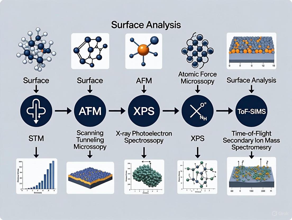
Comparative Analysis of Surface Analysis Methods for Electronic Properties: Techniques, Applications, and Future Directions in Biomedical Research
This comprehensive review examines the capabilities, applications, and limitations of major surface analysis techniques for characterizing electronic properties in biomedical and materials research.
Comparative Analysis of Surface Analysis Methods for Electronic Properties: Techniques, Applications, and Future Directions in Biomedical Research
Abstract
This comprehensive review examines the capabilities, applications, and limitations of major surface analysis techniques for characterizing electronic properties in biomedical and materials research. Covering X-ray photoelectron spectroscopy (XPS), ultraviolet photoelectron spectroscopy (UPS), scanning tunneling microscopy (STM), atomic force microscopy (AFM), and related methods, we explore how these tools provide critical insights into surface composition, electronic structure, band gaps, and work function. With increasing demand for precise surface characterization in semiconductor devices, drug delivery systems, and medical implants, this analysis helps researchers select appropriate methodologies, optimize experimental parameters, and interpret electronic property data for advanced material development and biomedical applications. The integration of AI and machine learning with traditional surface analysis techniques represents a significant advancement for data interpretation and automation in electronic property characterization.
Understanding Surface Electronic Properties: Fundamental Concepts and Measurement Principles
The Critical Role of Surface Electronic Properties in Material Performance and Biomedical Applications
The performance of functional materials, especially in biomedical and electronic applications, is not solely governed by their bulk composition but is critically determined by the atomic and molecular layers at the surface. Surface electronic properties, such as work function, ionization potential, and electron affinity, directly control a material's interactions with its biological environment, influencing charge transfer, catalytic activity, and biocompatibility [1] [2]. In biomedical devices, these interactions dictate everything from the fidelity of neural signal recording to the specificity of biosensors and the long-term stability of implants [3].
The growing sophistication of materials science necessitates a deep understanding of these surface characteristics. This guide provides a comparative analysis of the primary experimental techniques used to investigate surface electronic properties, detailing their methodologies, applications, and performance in a biomedical context. It aims to equip researchers with the knowledge to select the optimal characterization strategy for developing advanced biomedical materials, from neural interfaces to diagnostic biosensors.
Comparative Analysis of Surface Analysis Techniques
A range of sophisticated techniques is available for probing surface electronic properties. The choice of technique depends on the specific electronic parameter of interest, the material system, and the required resolution. The following table summarizes the core techniques dedicated to electronic property analysis.
Table 1: Core Techniques for Surface Electronic Property Analysis
| Technique | Primary Measured Electronic Properties | Key Principle | Best for Material Types |
|---|---|---|---|
| Ultraviolet Photoelectron Spectroscopy (UPS) | Valence Band Structure, Work Function, Ionization Potential [1] | Low-energy UV photons eject electrons from valence levels for high-resolution analysis of occupied states [1]. | Organic semiconductors, conductive polymers, metals. |
| Low-energy Inverse Photoemission Spectroscopy (LEIPS) | Unoccupied Electronic States, Electron Affinity, Conduction Band [1] | Analyzes unoccupied states by probing the conduction band, crucial for understanding charge transport [1]. | Beam-sensitive materials like organic semiconductors. |
| Reflection Electron Energy Loss Spectroscopy (REELS) | Optical Band Gaps, Hydrogen Content, Carbon Hybridization [1] | Provides optical and chemical information by measuring energy loss of electrons reflected from the surface [1]. | Semiconductors, thin films, hydrogen storage materials. |
| X-ray Photoelectron Spectroscopy (XPS) | Surface Composition, Chemical States, Empirical Electronic State [1] | X-rays eject core-level electrons, providing quantitative atomic composition and chemical state information [1]. | Virtually all solid materials; provides complementary chemical data. |
Modern integrated instruments often combine these techniques to provide a holistic view of a material's electronic structure. For instance, combining UPS and LEIPS allows for the analysis of the full electronic band gap, while REELS provides insight into optical and dielectric properties [1].
The Complementary Role of Compositional and Morphological Analysis
While this guide focuses on electronic properties, a complete surface analysis integrates electronic data with compositional and morphological information. Techniques like Scanning Electron Microscopy (SEM) and Atomic Force Microscopy (AFM) are indispensable for correlating electronic performance with physical structure [2].
Table 2: Complementary Surface Characterization Techniques
| Technique | Primary Function | Spatial Resolution | Application in Biomedical Materials |
|---|---|---|---|
| X-ray Photoelectron Spectroscopy (XPS) | Elemental Composition & Chemical State Analysis [2] | ~10 µm | Verifying surface chemistry of biosensor coatings [1]. |
| Atomic Force Microscopy (AFM) | 3D Surface Topography & Nanomechanical Mapping [4] | <1 nm | Measuring roughness of neural electrodes to assess cell adhesion [3] [5]. |
| Scanning Electron Microscopy (SEM) | High-Resolution Surface Imaging [4] | <1 nm | Visualizing porous structures in drug delivery carriers [2]. |
| Contact Angle Goniometer | Surface Wettability & Free Energy [4] | N/A | Quantifying hydrophilicity/hydrophobicity for biocompatibility [5]. |
The following workflow diagram illustrates how these techniques can be integrated into a comprehensive materials development strategy for biomedical applications.
Diagram 1: A workflow for developing biomedical materials through integrated surface analysis. This correlative approach links electronic, chemical, and morphological data to functional performance.
Experimental Protocols for Key Techniques
This section outlines detailed methodologies for conducting key experiments cited in this guide, ensuring reproducibility and reliable data acquisition.
Protocol: Electronic Property Analysis via UPS/LEIPS
Objective: To determine the complete electronic band structure (work function, ionization potential, electron affinity, and band gap) of a thin-film organic semiconductor for biosensor applications [1].
Materials:
- Integrated XPS/UPS/LEIPS system (e.g., PHI XPS instrument).
- Sample holder and charge-neutralizing flood gun.
- He I (21.22 eV) or He II (40.8 eV) UV source for UPS.
- Low-energy electron gun for LEIPS.
- High-resolution electron energy analyzer.
Procedure:
- Sample Preparation: Spin-coat or vapor-deposit the material onto a conductive substrate (e.g., ITO). Ensure the sample is clean and dry. Mount securely on the sample holder.
- Load and Pump-Down: Introduce the sample into the ultra-high vacuum (UHV) analysis chamber. Evacuate to a base pressure typically below 5 × 10⁻⁹ Torr to prevent surface contamination.
- UPS Measurement: a. Align the UV source and analyzer. Set the sample bias to -5 to -10 V to observe the secondary electron cutoff. b. Acquire the UPS spectrum in the cutoff region to calculate the work function. c. Acquire the valence band region with high resolution to determine the density of occupied states and the valence band maximum.
- LEIPS Measurement: a. Switch to the LEIPS setup with the low-energy electron gun. b. Excite the sample with electrons of known kinetic energy (typically 0-20 eV). c. Detect the emitted photons to measure the density of unoccupied states and the conduction band minimum.
- Data Analysis:
- Work Function: Subtract the width of the UPS spectrum (from Fermi edge to cutoff) from the photon energy.
- Band Gap: Calculate the energy difference between the conduction band onset (from LEIPS) and the valence band maximum (from UPS).
Protocol: Functionalization of a Graphene-Based Neural Electrode
Objective: To enhance the performance and biocompatibility of a graphene bioelectrode for high-fidelity neural signal detection, as referenced in the "Large-area NeuroWeb" (LNW) probe study [3].
Materials:
- Graphene film on a flexible substrate (e.g., polyimide).
- Hexagonal Boron Nitride (h-BN) encapsulation layers.
- Conductive polymer solution (e.g., PEDOT:PSS).
- Plasma cleaner (O₂/Ar gas).
- Electrochemical deposition setup.
Procedure:
- Surface Cleaning and Activation: Place the graphene electrode in a plasma cleaner. Treat with O₂ plasma for 1-2 minutes to create functional groups (-OH, -COOH) on the surface, improving hydrophilicity and adhesion.
- Encapsulation: Transfer or deposit ultra-thin layers of h-BN onto the graphene surface. This h-BN/Gr/h-BN architecture provides electrical insulation and protects the graphene from the biological environment while maintaining flexibility [3].
- Electrochemical Functionalization (Optional): a. Immerse the electrode in a PEDOT:PSS solution in a three-electrode electrochemical cell. b. Use cyclic voltammetry or potentiostatic deposition to coat the graphene surface with a nanoscale layer of the conductive polymer. This step reduces impedance and improves charge injection capacity [3].
- Validation: Characterize the modified electrode using AFM for morphology, XPS for surface chemistry, and electrochemical impedance spectroscopy (EIS) to verify performance enhancement.
The Scientist's Toolkit: Essential Research Reagents & Materials
The following table lists key materials and reagents critical for research and development in surface-engineered biomedical materials.
Table 3: Essential Research Reagents and Materials for Surface Engineering
| Material/Reagent | Function in Research | Key Application Example |
|---|---|---|
| Graphene & Carbon Nanotubes | Conductive nanomaterial for electrode sites and pathways; provides high specific surface area and biocompatibility [3]. | Flexible cortical electrodes for neural signal recording [3]. |
| Transition Metal Oxides (TMOs) | Versatile nanomaterials with unique catalytic, electronic, and optical properties [6]. | Iron oxide (Fe₃O₄) for MRI contrast agents; Zinc oxide (ZnO) for electrochemical biosensors [6]. |
| Conductive Polymers (e.g., PEDOT:PSS) | Interface modification layer to reduce electrochemical impedance and improve charge transfer at the bio-electrode interface [3]. | Coating on neural probes to enhance signal-to-noise ratio [3]. |
| Hexagonal Boron Nitride (h-BN) | 2D insulating encapsulation layer; provides chemical stability and protection for sensitive electronic materials in biological fluids [3]. | Encapsulation of graphene in ultra-thin neural probes [3]. |
| Silver Molybdate (β-Ag₂MoO₄) | Semiconductor material whose surface termination and work function can be engineered for specific electronic and photocatalytic activity [7]. | Potential application in photodynamic therapy or antimicrobial surfaces. |
The critical role of surface electronic properties is a unifying theme across the advancement of biomedical materials. From enabling the high-sensitivity detection of neural action potentials with graphene interfaces [3] to dictating the catalytic efficiency of transition metal oxides in biosensors [6], a fundamental understanding of these properties is non-negotiable. The experimental frameworks and comparative data presented in this guide underscore the power of a multimodal analytical approach. By strategically employing and correlating data from techniques like UPS, LEIPS, XPS, and AFM, researchers can transcend traditional trial-and-error methods. This systematic, insight-driven development is the key to engineering next-generation surfaces that will power the future of wearable medical devices, advanced diagnostics, and personalized health management systems.
Comparative Analysis of Surface Analysis Methods for Electronic Properties Research
The development of advanced materials for applications in electronics, catalysis, and energy conversion hinges on a deep understanding of key electronic parameters. Work function, band gap, surface potential, and the broader electronic structure dictate material behavior in devices and reactions. This guide provides a comparative analysis of the predominant experimental and computational methods used to characterize these properties, equipping researchers with the data needed to select the optimal technique for their specific material system.
Quantitative Comparison of Key Electronic Parameters
The electronic properties of a material are not absolute but can vary significantly with surface chemistry and structure. The following tables summarize core parameters for selected materials and the capabilities of different characterization techniques.
Table 1: Experimentally Determined Electronic Parameters of Selected Materials
| Material | Band Gap (eV) | Ionization Potential (eV) | Work Function (eV) | Surface Termination/Notes |
|---|---|---|---|---|
| β-TaON (111)_O surface [8] | 2.30 | - | - | Most stable surface termination |
| β-TaON (100)_O surface [8] | 2.20 | - | - | - |
| MnPS3 [9] | - | 6.0 | - | Suitable for HER and OER |
| FePS3 [9] | - | 5.4 | - | Lowest ionization potential in MPS3 series |
| CoPS3 [9] | - | 6.1 | - | - |
| NiPS3 [9] | - | 6.2 | - | Highest ionization potential in MPS3 series |
Table 2: Comparison of Primary Surface Analysis Techniques
| Technique | Key Measured Parameters | Spatial Resolution | Key Strengths | Primary Limitations |
|---|---|---|---|---|
| Kelvin Probe Force Microscopy (KPFM) | Surface Potential, Work Function | Nanoscale | Most suitable technique for work function mapping; high spatial resolution [10]. | Measures contact potential difference, not absolute work function. |
| X-ray Photoelectron Spectroscopy (XPS) | Elemental Composition, Chemical State, Ionization Potential, Valence Band Maximum | 10s of µm | Provides detailed chemical state information; can determine ionization potential [9]. | Lower spatial resolution than microscopy techniques; requires ultra-high vacuum. |
| UV Photoelectron Spectroscopy (UPS) | Work Function, Ionization Potential, Valence Band Structure | 10s of µm | Direct method for measuring work function and valence band density of states [9]. | Limited probing depth; requires ultra-high vacuum. |
| Scanning Tunneling Microscopy (STM) | Surface Topography, Local Density of States | Atomic-scale | Unparalleled atomic-scale resolution for conductive surfaces [11]. | Requires conductive samples. |
| Atomic Force Microscopy (AFM) | Surface Topography, Mechanical Properties | Nanoscale | Versatile; works on conductive and insulating samples [12]. | Does not directly provide chemical or electronic state information. |
| Density Functional Theory (DFT) | Work Function, Band Structure, Surface DOS | Atomic-scale (Computational) | Predicts highest and lowest work functions; provides atomic-level insights [10] [13]. | High computational cost; accuracy depends on chosen functionals. |
Experimental Protocols for Key Methodologies
A rigorous comparison requires an understanding of the standard protocols for obtaining the data presented.
DFT+U Computational Protocol for Surface Properties
This protocol is used for predicting work functions and band alignment of surfaces, as exemplified in the study of β-TaON [8].
- Computational Framework: Calculations are performed using periodic DFT with a plane-wave basis set, as implemented in codes like Quantum ESPRESSO.
- Exchange-Correlation Functional: The Generalized Gradient Approximation (GGA) with the Perdew-Burke-Ernzerhof (PBE) functional is typically selected.
- Electron Interaction (U parameter): A Hubbard U parameter is added to the standard DFT (DFT+U) to more accurately describe the strongly correlated d and f electrons, which is critical for correct band gap prediction.
- Pseudopotentials: Ultra-soft pseudopotentials are used to replace core electrons, balancing computational accuracy and efficiency.
- Surface Modeling: Surfaces are modeled as slab structures with a sufficient thickness of atomic layers and a vacuum layer of ~15 Å to prevent interactions between periodic images.
- Property Calculation:
- Work Function: Calculated as the energy difference between the electrostatic potential in the vacuum region and the Fermi energy.
- Band Alignment: Determined by calculating the valence band maximum and conduction band minimum positions relative to the vacuum level.
Combined XPS/UPS Experimental Protocol for Band Alignment
This methodology determines key electronic properties like ionization potential and work function experimentally, as used for MPS3 crystals [9].
- Sample Preparation: High-quality crystals are exfoliated in situ under ultra-high vacuum (UHV) to obtain pristine, contaminant-free surfaces for measurement. The purity of the sample is verified via survey XPS scans.
- XPS Measurement:
- Purpose: To confirm chemical composition and purity.
- Procedure: A wide-scan spectrum is collected to identify all elements present. High-resolution scans of core-level peaks (e.g., Ni-2p, S-2p, P-2p for NiPS3) are then fitted to confirm the chemical state and the absence of oxide or other contaminant peaks.
- UPS Measurement:
- Purpose: To determine the work function and ionization potential.
- He I photons (21.2 eV) are used as the excitation source.
- Work Function: Measured by subtracting the width of the UPS energy distribution (from the secondary electron cutoff to the Fermi edge) from the photon energy.
- Ionization Potential: Determined by linearly extrapolating the leading edge of the UPS spectrum in the valence band region to the background, which gives the energy from the vacuum level to the valence band maximum.
- Optical Absorption Measurement:
- Purpose: To determine the optical band gap.
- Procedure: Room-temperature absorption spectra are collected. The band gap is identified from the onset of absorption, often corresponding to charge-transfer or d-d transitions.
- Electron Affinity is subsequently calculated as the difference between the ionization potential and the optical band gap.
The logical workflow for this multi-technique experimental approach is outlined below.
The Scientist's Toolkit: Essential Research Reagents & Materials
Successful characterization relies on high-quality materials and specialized instruments.
Table 3: Essential Materials and Instruments for Surface Analysis Research
| Item | Function/Application |
|---|---|
| High-Purity Single Crystals | Base material for fundamental studies; required for exfoliation to create pristine surfaces for XPS/UPS [9]. |
| Ultra-High Vacuum (UHV) System | Essential environment for XPS and UPS to prevent surface contamination and enable electron detection [9]. |
| Monochromatic X-ray Source (Al Kα) | Standard excitation source for XPS to probe elemental composition and chemical states [12]. |
| He I UV Source (21.2 eV) | Standard excitation source for UPS to probe the valence band region and work function [9]. |
| Conductive Substrates (e.g., Si wafers) | Used for mounting powder or insulating samples to mitigate charging effects during XPS/UPS measurements. |
| DFT Simulation Software (e.g., Quantum ESPRESSO) | Open-source software package for first-principles calculations of material properties, including electronic structure [8]. |
Advanced & Emerging Methodologies
The field is rapidly advancing with new computational and integrated approaches.
High-Throughput Computational Framework
Obtaining accurate surface electronic properties like the density of states (DOS) via slab-based DFT is computationally expensive. A emerging framework addresses this bottleneck [13].
- Principle: A data-driven model is trained to predict the surface DOS directly from the bulk DOS, bypassing the need for explicit, costly surface calculations.
- Protocol:
- Data Generation: Bulk and surface DOS are calculated for a small set of reference compounds (e.g., CuNbS, CuTaS, CuVS) using DFT.
- Dimensionality Reduction: Principal Component Analysis (PCA) is applied to compactly represent both bulk and surface DOS data.
- Linear Mapping: A transformation matrix is trained to map the latent features of the bulk DOS to those of the surface DOS using the reference compounds.
- Prediction: The trained model is applied to new, unseen compositions (e.g., CuCrS, CuMoS) to predict their surface DOS.
This high-throughput framework enables the rapid screening of surface electronic properties across a wide chemical space.
Integration of AI and Machine Learning
The integration of artificial intelligence is revolutionizing surface analysis data interpretation and instrument operation [11] [10].
- AI-Enabled Data Analysis: Instrument manufacturers are now offering software that uses machine learning (ML) and deep learning (DL) for automated analysis of complex spectral data, improving speed and reproducibility [11].
- Machine Learning for Work Function Prediction: Combined Bayesian machine learning and first-principles approaches (CBMLFP) are showing great promise for predicting the lowest and highest work functions of materials with very low computational cost compared to traditional DFT [10].
The relationship between traditional and emerging computational methods is summarized in the following diagram.
The precise characterization of electronic properties at material surfaces and interfaces is a cornerstone of modern electronics, catalysis, and materials science. Surface analysis techniques provide critical insights into the elemental composition, chemical state, and electronic structure that govern device performance. The global surface analysis market, projected to reach USD 9.19 billion by 2032, reflects the growing importance of these techniques across semiconductors, energy storage, and quantum materials research [11].
For electronic applications, even minor surface contaminants or atomic-scale reconstructions can dramatically alter work function, carrier concentration, and interface conductivity. Techniques ranging from X-ray photoelectron spectroscopy to scanning probe microscopies have become indispensable for developing advanced semiconductors, novel catalysts, and next-generation energy storage systems. This guide provides a comparative analysis of major surface analysis techniques, with a specific focus on their applications for characterizing electronic properties.
Comparative Analysis of Major Techniques
The selection of an appropriate surface analysis technique depends critically on the specific electronic property of interest, required resolution, and material system. Each method provides unique insights into different aspects of surface and interface electronic structure.
Table 1: Key Surface Analysis Techniques for Electronic Property Characterization
| Technique | Principle of Operation | Lateral Resolution | Depth Sensitivity | Key Electronic Properties Measured |
|---|---|---|---|---|
| XPS (X-ray Photoelectron Spectroscopy) | Measures kinetic energy of photoelectrons ejected by X-ray irradiation [14] | ~10 µm (lab); ~100 nm (synchrotron) | 1-10 nm [14] | Elemental composition, chemical state, oxidation states, work function, valence band structure |
| STM (Scanning Tunneling Microscopy) | Measures quantum tunneling current between sharp tip and conductive surface [11] | Atomic resolution (0.1 nm) [11] | Surface atomic layer (0.5-1 nm) | Surface topography, local density of states (LDOS), band gap, charge density waves, spin polarization |
| SEM (Scanning Electron Microscopy) | Detects secondary/backscattered electrons from electron beam-specimen interactions [14] | 1-10 nm (resolution); 1 nm (field emission) [15] | 100 nm - 1 µm (depends on beam energy) | Surface morphology, grain boundaries, defect structures, voltage contrast, electron channeling patterns |
| TEM/STEM (Transmission Electron Microscopy/ Scanning TEM) | Transmits high-energy electrons through thin specimens [15] | ~0.05 nm (TEM); ~0.1 nm (STEM) [15] | Sample thickness dependent (typically 50-500 nm) | Atomic structure, defects, strain fields, elemental mapping (via EDS/EELS), electronic structure via EELS |
| AFM (Atomic Force Microscopy) | Measures forces between sharp tip and surface [16] | Atomic resolution (0.1 nm) vertical; 1 nm lateral | Surface atomic layer | Surface topography, work function (KPFM), surface potential, electrical conductivity (CAFM), piezoelectric response |
Quantitative Performance Comparison
Understanding the quantitative capabilities and limitations of each technique is essential for appropriate experimental design, particularly for electronic device characterization where different techniques may probe complementary aspects of the same system.
Table 2: Quantitative Performance Metrics for Electronic Property Characterization
| Technique | Energy Resolution | Detection Sensitivity | Typical Measurement Environment | Data Acquisition Time | Key Limitations for Electronic Characterization |
|---|---|---|---|---|---|
| XPS | 0.1-1.0 eV | 0.1-1 at% | Ultra-high vacuum (UHV) required [17] | Minutes to hours | Limited spatial resolution; requires good vacuum; primarily surface composition (not direct electronic function) |
| STM | ~1 meV (spectroscopy) | Single atoms | UHV, air, or liquid possible | Seconds to minutes per image | Requires conductive samples; measures electronic structure indirectly via tunneling |
| SEM | N/A (imaging) | N/A (morphology) | High vacuum typically | Seconds to minutes | Limited chemical/electronic information without attachments; sample charging for insulating materials |
| TEM/STEM | 0.1-1.0 eV (EELS) | Single atoms with advanced detectors | High vacuum | Minutes to hours | Complex sample preparation (thin sections); potential beam damage; indirect electronic property measurement |
| AFM | N/A (force: pN) | Single atoms (topography) | UHV, air, or liquid possible | Minutes per image | Lower scan speed than SEM; tip convolution effects; possible tip-induced surface modification |
Experimental Approaches and Methodologies
Standardized Experimental Protocols
Reproducible surface analysis requires careful attention to experimental protocols across different techniques. Standardized methodologies ensure comparable results and meaningful interpretation of electronic properties.
XPS Protocol for Work Function and Valence Band Analysis:
- Sample Preparation: Clean specimen surface via Ar+ sputtering (1-4 keV, 5-15 minutes) to remove adventitious carbon, followed by brief annealing if appropriate for the material.
- Instrument Calibration: Verify energy scale using Au 4f7/2 peak (84.0 eV) or Cu 2p3/2 peak (932.7 eV) for conductive samples.
- Data Acquisition:
- Survey spectrum (0-1100 eV binding energy, 1 eV steps, 50-100 eV pass energy)
- High-resolution regional scans (20 eV window, 0.1 eV steps, 20-50 eV pass energy)
- Valence band region (0-30 eV binding energy, 0.05 eV steps, 10-20 eV pass energy)
- Work Function Measurement: Use ultraviolet photoelectron spectroscopy (UPS) mode with He I (21.22 eV) or He II (40.8 eV) radiation, measuring secondary electron cutoff and Fermi edge.
- Data Analysis: Subtract Shirley or Tougaard background, fit peaks with Gaussian-Lorentzian functions, correct for charging using adventitious C 1s peak (284.8 eV) for insulating samples.
STM Protocol for Local Density of States Mapping:
- Tip Preparation: Electrochemically etch tungsten or PtIr wire to sharp apex, clean via in-situ electron bombardment or field emission.
- Sample Preparation: Cleave, sputter, or anneal in UHV to obtain atomically clean surface, verify cleanliness with Auger or XPS.
- Approach and Engagement: Approach tip to surface using coarse motor and fine piezoelectric control until tunneling current established (typically 0.1-2 nA at 0.1-2 V).
- Imaging Parameters: Constant current mode for topography (feedback loop maintains setpoint current), set bias voltage and current appropriate for material (metals: 0.1-1 V, 0.5-2 nA; semiconductors: 1-3 V, 0.1-0.5 nA).
- dI/dV Spectroscopy: At fixed location, open feedback loop, sweep bias voltage while measuring current, use lock-in detection with small AC modulation (5-20 mV, 1-5 kHz) to obtain dI/dV (proportional to LDOS).
Integrated Workflow for Comprehensive Surface Characterization
A multi-technique approach provides the most complete understanding of complex electronic materials. The following workflow represents an integrated methodology for correlative surface analysis:
Workflow Description: This integrated approach begins with macro-scale characterization (SEM, XPS) to identify regions of interest, followed by nano-to-atomic scale analysis (STM, TEM) of specific features. The correlative data integration enables direct relationships between surface composition, morphology, and electronic properties.
Advanced Applications and Emerging Methods
Cutting-Edge Applications in Electronics Research
Advanced surface analysis techniques are driving innovations across multiple electronics domains:
Semiconductor Development: The semiconductor industry accounts for approximately 29.7% of the surface analysis market, driven by demands for miniaturization and interface control [11]. TEM and STEM techniques enable atomic-scale imaging of transistor interfaces, gate oxides, and dopant distributions. Recent advances in 4D-STEM allow mapping of electric fields and charge distributions in operating devices, providing insights into carrier transport and failure mechanisms [18].
Quantum Materials: STM has been crucial for characterizing topological insulators, quantum spin liquids, and unconventional superconductors. By combining topography with dI/dV mapping, researchers can visualize superconducting gaps, charge density waves, and topological surface states with atomic resolution. Cryogenic STM systems operating below 1 K enable the study of quantum phenomena inaccessible at higher temperatures.
Energy Materials: In-situ TEM and XPS techniques are revolutionizing the study of battery interfaces, fuel cell catalysts, and photovoltaic materials. AP-XPS (ambient pressure XPS) allows investigation of solid-gas and solid-liquid interfaces under operational conditions, revealing potential-dependent chemical states during electrocatalysis [17]. These insights guide the development of more efficient energy conversion and storage systems.
Emerging Trends and Methodological Innovations
The field of surface analysis is rapidly evolving with several key trends shaping future capabilities:
Multimodal Correlative Microscopy: Integration of multiple techniques on a single platform provides complementary information from the same region. For example, combined SEM-Raman-AFM systems correlate morphological features with chemical composition and mechanical properties. Similarly, TEM with XPS and APT (atom probe tomography) enables correlation of atomic structure with 3D chemical mapping [18] [19].
In-situ and Operando Characterization: There is growing emphasis on studying materials under realistic operating conditions rather than in idealized vacuum environments. In-situ TEM with electrical biasing, heating, and gas/liquid environments reveals dynamic structural and chemical changes during device operation [20]. These approaches bridge the "materials gap" between fundamental studies and practical applications.
AI-Enhanced Data Analysis: Machine learning and artificial intelligence are transforming data interpretation across surface analysis techniques. AI algorithms automate feature identification, enhance signal-to-noise ratios, and extract subtle correlations from large multidimensional datasets [11]. For example, deep learning approaches can reconstruct atomic structures from noisy TEM images or identify defect types in SEM images with human-level accuracy.
High-Throughput Characterization: Automated sample handling, data acquisition, and analysis pipelines enable rapid screening of material libraries. This approach accelerates materials discovery and optimization, particularly for complex multi-component systems where composition-structure-property relationships are not easily predicted.
Essential Research Reagent Solutions
Successful surface analysis requires specialized materials and calibration standards to ensure accurate, reproducible results. The following table outlines essential research reagents and their applications:
Table 3: Essential Research Reagents and Materials for Surface Analysis
| Reagent/Material | Primary Function | Application Examples | Key Considerations |
|---|---|---|---|
| Reference Materials (Au, Ag, Cu) | Energy scale calibration | XPS, AES calibration using Au 4f7/2 (84.0 eV), Ag 3d5/2 (368.3 eV), Cu 2p3/2 (932.7 eV) | High purity (>99.99%), clean surface preparation via sputtering |
| Conductive Adhesives/Cements | Sample mounting for SEM/TEM/XPS | Carbon tape, silver paste, copper tape for electrical grounding | Low outgassing in vacuum, minimal elemental interference |
| Sputter Coating Materials | Conductive coatings for insulating samples | Au/Pd (5-10 nm) for high-resolution SEM, C for EDS, Cr for high-magnification | Thickness control to avoid obscuring fine surface features |
| FIB/SEM Preparation Supplies | Site-specific sample preparation for TEM/APT | Gallium ion sources, micromanipulators, deposition gases (Pt, W) | Minimizing ion beam damage, contamination control |
| Calibration Gratings | Lateral dimension calibration | STM/AFM/SEM magnification verification using 1D/2D gratings | Traceable to NIST standards, appropriate pitch for resolution verification |
| XPS Charge Compensation Standards | Referencing for insulating samples | Adventitious carbon (C 1s at 284.8 eV), deposited Au nanoparticles | Consistency in application, minimal sample contamination |
Surface analysis techniques provide indispensable tools for characterizing electronic properties at material interfaces, with each method offering unique strengths and limitations. XPS delivers quantitative chemical state information, STM provides unparalleled atomic-scale electronic structure mapping, SEM offers high-resolution morphological imaging, and TEM reveals atomic structure and composition. The growing integration of these techniques through correlative approaches, combined with advances in in-situ characterization and AI-enhanced analysis, is creating unprecedented opportunities for understanding and designing advanced electronic materials. As semiconductor devices continue to shrink and quantum materials become increasingly complex, sophisticated surface analysis will remain essential for linking atomic-scale structure to electronic function.
This guide provides an objective comparison of the primary surface analysis techniques—Photoemission, Tunneling, and Force Interactions—used for investigating electronic properties in materials science and drug development research.
Core Principles and Physical Interactions
The fundamental physics of electronic property measurement techniques dictates their specific applications, strengths, and limitations.
Photoemission Spectroscopy (XPS) relies on the photoelectric effect. A sample is irradiated with X-rays, causing the ejection of core-level photoelectrons. The kinetic energy of these electrons ((E{KE})) is measured and related to their binding energy ((E{BE})) through the equation (E{KE} = h \nu - E{EB} - \Phiw), where (h \nu) is the X-ray photon energy and (\Phiw) is the spectrometer's work function [21]. This process provides detailed information about the elemental composition and chemical state of the surface.
Scanning Tunneling Microscopy/Spectroscopy (STM/STS) is based on the quantum mechanical phenomenon of electron tunneling. When a sharp metallic tip is brought within atomic proximity (typically <1 nm) of a conductive surface, a bias voltage applied between them allows electrons to tunnel through the vacuum barrier. The tunneling current is exponentially sensitive to the tip-sample separation, enabling atomic-scale resolution imaging. STS extends this capability by measuring the local density of states (LDOS) at the surface, providing direct information on electronic structure, band gaps, and surface metallicity [22] [23].
Atomic Force Microscopy (AFM) measures force interactions between a nanoscale tip and the sample surface. The tip is mounted on a flexible cantilever, and as it scans the surface, interatomic forces (e.g., van der Waals, chemical, electrostatic) cause cantilever deflection. This deflection is measured, typically with a laser beam, to reconstruct surface topography with nanometer resolution. Unlike STM, AFM does not require a conductive sample, making it suitable for polymers and biological materials [12].
Diagram 1: Fundamental physical interactions underlying major surface analysis techniques for electronic property measurement.
Comparative Performance Analysis
The following tables summarize the quantitative performance metrics, applications, and limitations of each technique based on current market data and experimental capabilities.
Table 1: Quantitative Performance Metrics of Surface Analysis Techniques
| Technique | Information Depth | Lateral Resolution | Element Sensitivity | Data Acquisition Speed |
|---|---|---|---|---|
| XPS | 3-10 monolayers (≈10 Å) [24] [21] | 5-10 µm (lab-based); <100 nm (synchrotron) | All elements except H; detection limits ~0.1 at% [21] | Minutes to hours for high-resolution spectra |
| STM/STS | 1-2 atomic layers (atomic resolution) [11] [23] | Atomic-scale (≤1 Å) [11] | Not directly elemental; highly sensitive to local DOS | Seconds per image scan; point spectroscopy in seconds |
| AFM | Surface topography | ~1 nm (non-atomic) [12] | No direct elemental identification; mechanical/electronic properties | Minutes per image scan; slower than SEM |
| AES | 3-5 monolayers [21] | ≤10 nm [12] | Detection limits ~0.1-1 at% [12] | Faster than XPS for mapping |
| SIMS | 1-10 monolayers [24] [21] | 50-100 nm (dynamic); <1 µm (static) | ppb-ppm range for most elements [24] | Rapid data collection; depth profiling rate ~µm/min [24] |
Table 2: Application Suitability and Limitations in Electronic Property Research
| Technique | Key Strengths | Primary Limitations | Ideal Use Cases |
|---|---|---|---|
| XPS | Quantitative chemical state analysis; non-destructive [21] | Requires UHV; poor lateral resolution; insulating samples may charge [24] | Chemical composition of thin films; oxidation states; surface contamination [12] |
| STM/STS | Unparalleled atomic-scale resolution; direct electronic structure measurement [11] [23] | Requires conductive samples; limited to surfaces [22] | Atomic surface reconstruction; defect states; local density of states mapping [23] |
| AFM | Works on any material (conductive or insulating); various environmental conditions [12] | No direct chemical identification; slower scan speed; tip convolution | Polymer surface morphology; biological samples; nanomechanical property mapping [12] |
| AES | High spatial resolution; surface sensitivity; depth profiling [12] | Can cause beam damage; quantitative analysis challenging [12] | Failure analysis; microelectronics; thin film interfaces [12] |
| SIMS | Extreme sensitivity; isotope detection; depth profiling [24] [21] | Severe matrix effects; complex spectra; semi-destructive [24] | Trace element doping; semiconductor impurity analysis; organic surface layers [12] |
Experimental Protocols for Electronic Property Characterization
Scanning Tunneling Spectroscopy (STS) for Surface Electronic Structure
Objective: To measure the local density of states (LDOS) and identify metallic/semiconducting behavior of surfaces and nanostructures.
Methodology:
- Sample Preparation: A clean, atomically flat, and conductive surface is essential. For the Sn/Si(111) system, this involves repeated cycles of Ar⁺ sputtering (500 eV, 10-15 µA/cm²) followed by annealing at 1150-1200°C in ultra-high vacuum (UHV < 8×10⁻¹¹ mbar) to achieve the (√3×√3)R30° reconstruction. Sn is deposited from a Knudsen cell at 0.33 ML coverage [23].
- STM/STS Setup: The experiment is conducted in UHV at room temperature or low temperature (30-300 K) using an electrochemically etched W tip. The tip quality is verified by atomic resolution imaging on a reference surface like Si(111)-(7×7) [23].
- Spectroscopic Acquisition:
- Position the tip over the region of interest at a specific setpoint (e.g., Vₛ = 1.0 V, Iₛ = 0.5 nA).
- Disable the feedback loop to maintain fixed tip-sample separation.
- Ramp the bias voltage (e.g., from -2.0 V to +2.0 V) while measuring the tunneling current (I).
- Acquire multiple I-V curves at different locations to ensure reproducibility.
- Data Processing: The differential conductance (dI/dV), proportional to the LDOS, is obtained by numerical differentiation of I-V curves or directly via lock-in detection. The normalized conductance [dln(I)/dln(V)] is often calculated to minimize setpoint dependence [23].
Key Experimental Parameters (from Sn/Si(111) study [23]):
- Vacuum: < 8×10⁻¹¹ mbar
- Setpoint Voltages: 0.5 - 1.5 V
- Setpoint Currents: 0.2 - 1.0 nA
- Bias Range: -2.0 V to +2.0 V
Ultrafast Laser-Assisted Tunneling in Nanogaps
Objective: To investigate light-matter interactions in the tunneling regime and distinguish between optical rectification, hot-electron currents, and thermal effects.
Methodology:
- Junction Fabrication: Fabricate ultrastable metal-insulator-metal (MIM) tunnel junctions. For ITO/Lu₂O₃/Au junctions, grow epitaxial indium-tin-oxide (ITO) and lutetium oxide (Lu₂O₃) layers on yttria-stabilized zirconia (YSZ) substrates via pulsed laser deposition. The closely matched lattice constants ensure stability. Deposit a thin Au top electrode (≈20 nm) through a shadow mask [22].
- Electrical Characterization: Measure current-voltage (I-V) characteristics using a sourcemeter to confirm tunneling behavior. Verify exponential growth of |I| with increasing bias voltage (Vb) and exponential decay with increasing insulator thickness (d). For the d ≈ 2 nm junction, clear asymmetric I-V curves are observed due to dissimilar electrodes (ITO and Au) [22].
- Photoassisted Transport Measurements:
- Illuminate the junction with pulsed laser excitation across a broad wavelength range (e.g., 400-1350 nm).
- Measure the laser-induced current (photocurrent) using simple direct-current (DC) detection, enabled by the junction's exceptional stability.
- Systematically vary the insulating layer thickness, laser power, and wavelength.
- Mechanism Discrimination:
- Optical Rectification: Dominant at lower photon energies (>700 nm); manifests as a DC photocurrent that aligns with both classical and quantum descriptions of the tunneling process [22].
- Hot Electron Transport: Influences the process at high absorption or short wavelengths (<700 nm); electrons tunnel after gaining energy from photon absorption [22].
- Thermal Effects: Contribute to photocurrent generation through laser-induced heating, particularly at shorter wavelengths [22].
Diagram 2: Experimental workflow for Scanning Tunneling Spectroscopy (STS) to characterize surface electronic structure.
The Scientist's Toolkit: Essential Research Reagents & Materials
Table 3: Key Materials and Components for Surface Analysis Experiments
| Item | Function | Example Use Case |
|---|---|---|
| Conductive Single Crystals | Provide atomically flat, well-defined substrates for fundamental studies. | Si(111), Ge(111), Au(111) wafers for surface reconstruction studies [23]. |
| High-Purity Metal Evaporation Sources | Used in Knudsen cells for precise thermal deposition of ultrathin films. | Sn, Pb for creating group IV metal overlayers on semiconductor surfaces [23]. |
| Epitaxial Oxide Targets | Enable growth of high-quality, ultrathin insulating barriers in tunnel junctions. | Lu₂O₃, YSZ for stable metal-insulator-metal (MIM) junction fabrication [22]. |
| Electrochemically Etched Metal Wires | Form the sharp tips required for scanning probe microscopy. | W, PtIr tips for STM/STS measurements [23]. |
| Calibration Reference Materials | Standardize instrument performance and enable quantitative analysis. | NIST reference wafers for SEM/AFM calibration and contour extraction [11]. |
| UHV Sputter Ion Sources | Generate ion beams for sample cleaning and depth profiling. | Ar⁺ guns (500 eV - 5 keV) for surface preparation and cross-section analysis [23] [24]. |
| Monoenergetic X-ray Sources | Provide excitation photons for photoemission spectroscopy. | Mg Kα (1253.6 eV) and Al Kα (1486.6 eV) anodes for XPS analysis [21]. |
Emerging Trends and Future Outlook
The field of surface analysis is evolving with several key trends shaping its future. Integration of Artificial Intelligence and Machine Learning is enhancing data interpretation and automation, leading to improved precision and efficiency. Instrument manufacturers are now offering AI-enabled data analysis tools, such as JEOL's msFineAnalysis AI for automated structure analysis [11].
Computational advancements are enabling faster prediction of surface properties. Recent frameworks demonstrate that surface density of states (DOS) can be predicted directly from bulk electronic structure calculations using linear transformation models, potentially bypassing expensive slab-based density functional theory (DFT) simulations for high-throughput screening [13].
The push for miniaturization in semiconductors continues to drive demand for higher resolution techniques. The semiconductors segment is projected to hold a 29.7% share of the surface analysis market in 2025, requiring precise control over surface and interface properties at the nanometer scale [11]. Furthermore, sustainability initiatives are prompting more thorough surface evaluations to develop eco-friendly materials, contributing to the sector's growth [11].
The pursuit of advanced electronic devices is intrinsically linked to the precise control of material interfaces. The electronic behavior of components—from semiconductors to catalytic surfaces—is governed not merely by bulk properties but by atomic and molecular interactions at their surfaces and buried interfaces. Understanding this interplay between surface chemistry and electronic function is paramount for innovation in fields ranging from nanoelectronics to energy storage. This guide provides a comparative analysis of dominant surface analysis techniques, evaluating their efficacy in linking surface composition to electronic properties for researchers and scientists engaged in materials and device development.
The significance of this field is underscored by its growing market, valued at approximately USD 6.45 billion in 2025 and projected to reach USD 9.19 billion by 2032, demonstrating a compound annual growth rate (CAGR) of 5.18% [11]. This growth is propelled by the escalating demand for high-resolution imaging and precise material characterization across the semiconductor, automotive, and healthcare sectors [11] [12]. The materials science segment alone constitutes 23.8% of this market, highlighting its critical role in material innovation and characterization [11].
Comparative Analysis of Key Surface Analysis Techniques
Selecting the appropriate surface analysis technique is crucial for obtaining meaningful data about a material's surface composition and its corresponding electronic structure. The following section compares five prominent methods, summarizing their principles, applications, and specific utility in electronic properties research.
Table 1: Comparison of Primary Surface Analysis Techniques
| Technique | Primary Operating Principle | Key Applications in Electronics | Information Depth | Lateral Resolution |
|---|---|---|---|---|
| XPS (X-ray Photoelectron Spectroscopy) | Measures kinetic energy of photoelecters emitted by X-ray irradiation to determine elemental composition and chemical state [12]. | Thin film analysis, contaminant identification, surface chemistry of electronic materials [12]. | 1-10 nm [12] | 1-10 µm [12] |
| AES (Auger Electron Spectroscopy) | Analyzes kinetic energy of Auger electrons emitted from an atom after electron beam excitation to provide elemental composition [12]. | Studying thin films, interfaces, and nanostructures; identifying contaminants in semiconductors [12]. | 2-5 nm [12] | < 10 nm [12] |
| SIMS (Secondary Ion Mass Spectrometry) | Sputters surface with primary ion beam and analyzes mass-to-charge ratio of ejected secondary ions for elemental and isotopic composition [12]. | High-resolution depth profiling, detecting dopants and impurities in semiconductors [12]. | 1 nm - 1 µm [12] | 50 nm - 1 µm [12] |
| AFM (Atomic Force Microscopy) | Scans a sharp probe across the surface to measure forces, providing high-resolution 3D surface topography and mechanical properties [12]. | Studying surface morphology and mechanical properties of nanomaterials for electronics [12]. | Atomic-level (vertical) [12] | < 1 nm [12] |
| STM (Scanning Tunneling Microscopy) | Uses quantum tunneling current between a sharp tip and a conductive surface to image atomic-scale topography and electronic density [11]. | Visualizing atomic arrangement, defects, and electronic characteristics of conductive material surfaces [11]. | Atomic-level [11] | Atomic-level [11] |
Table 2: Comparative Performance in Electronic Property Analysis
| Technique | Sensitivity | Quantitative Accuracy | Best for Electronic Properties | Key Limitations |
|---|---|---|---|---|
| XPS | 0.1 - 1 at% [12] | High (with standards) [12] | Chemical state, oxidation state, band alignment studies [12] | Requires ultra-high vacuum; limited spatial resolution [12] |
| AES | 0.1 - 1 at% [12] | Moderate to High [12] | Interface composition, thin film quality, defect analysis [12] | Can cause electron beam damage; requires conductive samples [12] |
| SIMS | ppb - ppm range [12] | Semi-quantitative (with standards) [12] | Dopant distribution, impurity detection, depth profiling [12] | Complex data interpretation; matrix effects [12] |
| AFM | N/A (topographical) | N/A (topographical) | Surface roughness, domain structure, nanoscale electrical characterization (if conductive AFM) [12] | Slow scan speed; tip convolution effects [12] |
| STM | Single atoms [11] | N/A (topographical/electronic) | Atomic-scale surface topography, electron density maps, defect states [11] | Requires conductive samples; complex operation [11] |
Experimental Protocols and Methodologies
Case Study: Controlling Buried Interface Conductivity via Surface Termination
A seminal study from Pacific Northwest National Laboratory (PNNL) exemplifies the direct link between surface composition and electronic behavior. Researchers demonstrated that the hole conductivity at the buried interface between strontium titanium oxide (STO) and silicon (Si) could be controlled remotely by modifying the STO surface composition [25].
Experimental Workflow:
- Sample Preparation: High-quality STO thin films were epitaxially grown on Si substrates. The surface of the STO film was then modified with an ultrathin layer of specific atoms to alter its surface termination [25].
- Surface Composition Control: The key variable was the stability of extra oxygen at the STO surface. The native STO surface naturally attracts and traps oxygen, which acts as an electron trap [25].
- Electronic Property Measurement: The team used Hard X-ray Photoelectron Spectroscopy (HAXPES) to probe the electronic structure of the buried STO/Si interface. This technique is sensitive enough to analyze non-destructively through the material [25].
- Theoretical Modeling: Ab initio (first-principles) modeling was performed to understand the electronic charge redistribution driven by the surface composition [25].
Findings: The research established that surface-bound oxygen on STO draws electrons from the Si substrate. This transfer leaves behind a thin layer of positive charge (holes) in the Si, creating a conductive pathway. By adding a surface layer that prevents oxygen trapping, this electron transfer was impeded, thereby weakening or eliminating the conductive hole layer at the buried interface [25]. This is a powerful example of "functional cross talk" between a surface and a buried interface.
Protocol for Atomic-Scale Surface Characterization with STM
Scanning Tunneling Microscopy (STM) is unparalleled for directly correlating surface structure with electronic behavior at the atomic scale.
Experimental Methodology:
- Sample Requirement: The material must be electrically conductive. For semiconductors, this often requires a sufficiently doped substrate [11].
- Preparation: The sample surface must be atomically clean and flat. This is typically achieved in situ by cycles of sputtering (e.g., with Ar+ ions) and annealing (heating) under ultra-high vacuum (UHV) to remove contaminants and reconstruct the surface [11].
- Measurement:
- A sharp metallic tip (often tungsten or platinum-iridium) is brought within a nanometer of the sample surface.
- A bias voltage is applied between the tip and the sample, and the quantum tunneling current that flows is monitored.
- In constant-current mode, a feedback loop moves the tip up and down to maintain a set current, thus mapping the surface topography. The resulting image reflects both physical and electronic topography [11].
- Data Acquisition: Atomic-resolution images are obtained by scanning the tip raster-style across the surface. Spectroscopy modes (STS) can be performed by disabling the feedback loop and measuring current (I) as a function of voltage (V) at a specific location, providing local electronic density of states (LDOS) [11].
The Research Workflow: From Surface to Interface
The following diagram illustrates the logical workflow for establishing the relationship between surface composition and the electronic properties of a material or its buried interfaces, integrating the techniques discussed.
Diagram 1: Integrated Workflow for Interface Analysis
The Scientist's Toolkit: Essential Research Reagent Solutions
A successful investigation into surface and interface properties requires a suite of specialized tools and materials. The following table details key resources for such research.
Table 3: Essential Research Reagents and Materials for Surface Analysis
| Item / Solution | Function / Purpose | Example Use-Case |
|---|---|---|
| Reference Wafers | Standardized substrates for calibration of SEM/AFM instruments, ensuring cross-lab comparability and accurate contour extraction [11]. | Calibrating instrument response before measuring experimental semiconductor samples. |
| UHV Sputtering Sources | Sources of inert gas ions (e.g., Ar+) for in-situ cleaning of sample surfaces to remove contaminants and obtain atomically clean surfaces for analysis [11]. | Preparing clean STO or Si surfaces prior to STM or XPS analysis. |
| Conductive AFM Tips | Specially coated AFM probes (e.g., Pt/Ir or doped diamond) for measuring topography and simultaneous electrical properties like conductivity or surface potential [12]. | Mapping nanoscale current flow in organic semiconductor thin films. |
| HAXPES (Hard X-ray Photoelectron Spectroscopy) | A variant of XPS using higher energy X-rays to probe deeper layers and buried interfaces non-destructively [25]. | Analyzing the electronic structure of the buried STO/Si interface [25]. |
| AI-Enabled Data Analysis Tools | Software utilizing machine learning (ML) and deep learning (DL) for automated analysis of complex spectral and image data from techniques like SIMS and XPS [11]. | Automated structure analysis and peak identification in mass spectrometry data (e.g., JEOL's msFineAnalysis AI) [11]. |
The direct linkage between surface chemistry and electronic behavior is a cornerstone of modern materials science and electronics development. No single technique provides a complete picture; rather, a correlative approach that combines the chemical state information from XPS, the ultra-sensitive depth profiling of SIMS, the atomic-resolution imaging of STM, and the topological mapping of AFM is essential. As the field advances, the integration of artificial intelligence for data interpretation and the development of techniques capable of probing buried interfaces with higher fidelity, as demonstrated in the PNNL case study, will further empower researchers to design and control the electronic properties of next-generation materials with unprecedented precision.
Technique Deep Dive: Operational Principles and Specific Applications in Biomedical Research
X-ray Photoelectron Spectroscopy (XPS), also known as Electron Spectroscopy for Chemical Analysis (ESCA), stands as a cornerstone technique in modern surface science, providing unparalleled quantitative chemical state information from the topmost 1-10 nanometers of a material. [26] [27] This surface sensitivity, coupled with its ability to identify elemental composition and chemical bonding, makes XPS indispensable for researchers investigating electronic properties, catalytic processes, contamination, and material interfaces. The technique operates on the photoelectric effect, where irradiation by X-rays ejects photoelectrons from a material's surface; the kinetic energy of these electrons is measured and used to calculate their original binding energy, which is characteristic of specific elements and their chemical environments. [27] [28] Within the broader thesis of comparing surface analysis methods, XPS occupies a unique niche, offering superior chemical state identification compared to techniques like Auger Electron Spectroscopy (AES) and deeper, more chemically sensitive profiling than Secondary Ion Mass Spectrometry (SIMS) for many applications.
Comparative Analysis of Surface Analysis Techniques
The selection of an appropriate surface analysis technique is critical for electronic properties research. Each method offers distinct advantages and limitations in terms of elemental sensitivity, spatial resolution, and the type of information obtained. The following table provides a structured comparison of XPS against other prevalent surface analysis methods, highlighting its specific strengths in quantitative and chemical state analysis.
Table 1: Comparison of Major Surface Analysis Techniques for Electronic Properties Research
| Technique | Primary Information | Detection Limits (at%) | Depth Resolution / Sampling Depth | Chemical State Information? | Key Strengths | Major Limitations |
|---|---|---|---|---|---|---|
| XPS (ESCA) | Elemental composition, empirical formula, chemical state, electronic state [26] [27] [28] | 0.1 - 1.0% [27] [28] | ~10 nm (analysis depth); 20-200 Å (depth profiling) [28] | Yes, excellent [28] | Quantitative, chemical state ID, works with insulating samples [26] [28] | Poor lateral resolution (~10µm) [28], cannot detect H or He [27] |
| AES (Auger Electron Spectroscopy) | Elemental composition [12] | <0.1% (higher sensitivity for some elements) [12] | ~2-5 nm (analysis depth) [12] | Limited [12] | High spatial resolution, good for thin films and interfaces [12] | Can damage sensitive samples; quantitative analysis is challenging [12] |
| SIMS (Secondary Ion Mass Spectrometry) | Elemental & isotopic composition [12] | Parts per billion (ppb) to parts per million (ppm) [12] | Excellent (sub-nm for depth profiling) [12] | Limited (often lost during sputtering) [12] | Extreme sensitivity, depth profiling, all elements including H [12] | Destructive; quantification difficult; matrix effects [12] |
| AFM (Atomic Force Microscopy) | Surface topography, mechanical properties [11] [12] | N/A | Atomic-scale vertical resolution [11] | No | Atomic-scale resolution, measures mechanical properties, works in various environments [12] | No direct chemical information; slow scan speeds [12] |
| SEM (Scanning Electron Microscopy) | Surface morphology, composition (with EDX) [12] | ~0.1% (with EDX) [12] | Microns (interaction volume) [12] | No | High-resolution imaging, rapid analysis [12] | Little chemical state data; requires conductive coating for insulators [12] |
Market Adoption and Technological Trends
The surface analysis market reflects the critical importance of these techniques, with the global market expected to grow from USD 6.45 billion in 2025 to USD 9.19 billion by 2032, exhibiting a CAGR of 5.18%. [11] Within this landscape, the adoption of advanced technologies like XPS is driven by the expanding semiconductor, automotive, and healthcare sectors. [11] A key trend is the integration of artificial intelligence and machine learning for data interpretation and automation, which enhances precision and efficiency, thereby fueling market expansion. [11] Regionally, North America holds a dominant position with a 37.5% market share in 2025, while the Asia-Pacific region is projected to be the fastest-growing, driven by high industrialization and massive government research budgets in China, Japan, and South Korea. [11]
Experimental Protocols in XPS Analysis
A standard XPS analysis follows a structured workflow to extract comprehensive qualitative, quantitative, and chemical state data. The following diagram visualizes the key stages of this workflow.
Diagram 1: XPS Analysis Workflow. The process flows from sample preparation through broad survey scans to targeted high-resolution analysis and optional depth profiling.
Detailed Methodologies for Key XPS Modes
Survey Scan Analysis (Elemental Identification)
- Purpose: To identify and quantify all elements present on the surface (except hydrogen and helium). [27] [28]
- Protocol: A wide energy range scan (e.g., 0-1200 eV binding energy) is performed at high sensitivity. The resulting spectrum shows peaks corresponding to the electron configuration of the atoms present (e.g., 1s, 2s, 2p, 3s). The number of detected electrons in each peak is directly related to the amount of the element within the XPS sampling volume. [27] [28]
- Quantitative Analysis: To generate atomic percentage values, each raw XPS signal intensity is corrected by dividing by a relative sensitivity factor (RSF) and normalized over all detected elements. [27] Under optimal conditions, the quantitative accuracy for major peaks is 90-95% of the true value. [27]
High-Resolution Analysis (Chemical State Identification)
- Purpose: To determine the chemical bonding or oxidation state of the elements already identified. [28]
- Protocol: Narrow energy ranges encompassing specific core-level peaks (e.g., C 1s, O 1s, N 1s) are scanned under high energy resolution conditions. Chemical states are inferred from small shifts in the binding energy of the photoelectron peaks (chemical shifts) and changes in peak shape. [26] [27] [28]
- Data Processing: Peak fitting is performed on the high-resolution spectrum after subtracting a suitable background (e.g., Shirley or Tougaard background). Each component peak corresponds to a different chemical environment for the element.
Depth Profiling
- Purpose: To measure elemental composition as a function of depth, crucial for analyzing thin films, interfaces, and corrosion layers. [26] [29]
- Destructive Profiling Protocol: This is a cyclical process. The surface is first analyzed using high-resolution XPS scans. An ion beam (typically argon, either monatomic or cluster) is then used to sputter etch and remove a defined layer of material. The XPS analysis and sputtering steps are repeated until the desired depth is reached. [26] [29] [28]
- Non-Destructive Profiling (ARXPS): For the outer ~10-20 nm, Angle-Resolved XPS (ARXPS) can be used. This technique varies the emission angle at which electrons are collected, thereby changing the effective sampling depth without sputtering. This preserves chemical state information, which is often altered by ion bombardment during sputtering. [26] [28]
The Scientist's Toolkit: Essential Reagents & Materials
Table 2: Key Research Reagent Solutions for XPS Analysis
| Item / Solution | Function / Purpose | Critical Specifications |
|---|---|---|
| Mono-/Gas Cluster Ion Source | For depth profiling and surface cleaning. Gas cluster ion sources are essential for analyzing organic and polymeric materials previously inaccessible to profiling. [26] | MAGCIS dual-mode ion source; cluster sizes for soft materials. [26] |
| Charge Compensation Flood Gun | Neutralizes positive charge accumulation on electrically insulating samples (e.g., polymers, ceramics), preventing severe spectral distortion. [26] | Low-energy electrons; stabilization to within a few eV of neutral state. [26] |
| Reference Samples (Certified Standards) | For absolute quantification and instrument calibration. Required for high-accuracy compositional analysis. [27] | Homogeneous solid-state materials with known composition. [27] |
| X-ray Anodes | Source of X-ray photons for photoemission. Different anodes provide different photon energies. [26] | Al Kα (1486.7 eV), Mg Kα (1253.7 eV); monochromatic or non-monochromatic. [26] [27] |
| Conductive Adhesive Tapes | Mounting powdered or irregularly shaped samples to ensure electrical contact and minimize charging. | High-purity carbon or copper tapes. |
| UHV-Compatible Solvents | (e.g., Isopropanol, Methanol) For ultrasonic cleaning of samples prior to introduction into the ultra-high vacuum (UHV) chamber to prevent contamination. | High purity, low residue, volatile. |
Supporting Experimental Data & Case Applications
The quantitative capabilities of XPS are demonstrated across diverse research applications. In the semiconductor industry, XPS is critical for monitoring thin film composition, detecting contaminants at the parts-per-thousand level, and ensuring interface quality. [11] [12] For instance, XPS depth profiling can precisely measure the thickness and chemical composition of silicon dioxide (SiO₂) layers on silicon wafers, a fundamental structure in microelectronics. [28] In polymer science, XPS is used to quantify surface modifications, such as the introduction of oxygen-containing functional groups via plasma treatment, by tracking the change in the C 1s and O 1s high-resolution spectra. [28] A study on catalyst surfaces can use XPS to quantify the relative amounts of different oxidation states of a metal (e.g., Ce³⁺ vs. Ce⁴⁺) by deconvoluting the high-resolution spectrum, directly linking surface chemistry to catalytic activity. [29]
Table 3: Representative Quantitative XPS Data from a Thin Film Analysis
| Element | Binding Energy (eV) | Atomic % (Surface) | Atomic % (After 2 min Sputter) | Identified Chemical State |
|---|---|---|---|---|
| C 1s | 284.8 | 45.2 | 15.1 | C-C/C-H (Adventitious Carbon) |
| C 1s | 286.5 | 10.5 | 5.2 | C-O |
| O 1s | 530.1 | 25.3 | 40.8 | Metal Oxide (O²⁻) |
| O 1s | 531.8 | 15.1 | 8.5 | Hydroxyl/Adsorbed H₂O |
| Ti 2p₃/₂ | 458.5 | 4.0 | 30.4 | Ti⁴⁺ (TiO₂) |
| N 1s | 399.2 | 0.0 | 0.0 | Not Detected |
Within the comparative framework of surface analysis methods for electronic properties research, XPS establishes its indispensable role through its unique combination of quantitative elemental analysis and detailed chemical state identification. While techniques like SIMS offer superior detection limits and AES provides better spatial resolution, no other method provides the same level of robust, quantitative insight into surface chemistry as XPS. Its application spans from fundamental research in material science to rigorous quality control in the semiconductor and pharmaceutical industries. The ongoing technological advancements, including the development of gas cluster ion sources for superior depth profiling of soft materials and the integration of AI for data analysis, ensure that XPS will remain a critical tool for scientists and engineers pushing the boundaries of surface and interface science.
Ultraviolet Photoelectron Spectroscopy (UPS) is a powerful surface analysis technique specifically designed for investigating the electronic properties of materials. Operating on the same fundamental photoemission principle as X-ray Photoelectron Spectroscopy (XPS), UPS utilizes ultraviolet radiation to eject electrons, providing unique capabilities for probing valence band structures and measuring work functions with high precision [30]. Within the expanding surface analysis market, projected to reach USD 9.19 billion by 2032, UPS serves a critical niche in materials science and semiconductor research, complementing other techniques like Scanning Tunneling Microscopy (STM) and Atomic Force Microscopy (AFM) [11]. This guide objectively compares UPS performance against alternative methods, providing researchers with the experimental data and protocols needed to select the optimal technique for electronic properties characterization.
Technical Comparison of Surface Analysis Techniques
UPS occupies a specialized position within the surface analysis landscape, offering distinct advantages and limitations compared to other major techniques for electronic structure analysis.
Table 1: Comparison of Surface Analysis Techniques for Electronic Properties
| Technique | Primary Electronic Applications | Information Depth | Energy Resolution | Key Limitations |
|---|---|---|---|---|
| UPS | Valence band DOS, Work function, Surface electronic structure [31] [30] | 2-3 nm (Highly surface-sensitive) [30] | Very High (<20 meV possible) [32] | Restricted to conductors/semiconductors; Charging effects on insulators [33] [32] |
| XPS | Elemental composition, Chemical state, Valence band (wider peaks) [12] [30] | ~10 nm [30] | Moderate (0.3-1.0 eV) [32] | Lower resolution for valence states; Less sensitive to work function |
| STM | Surface topography, Local density of states (LDOS) at atomic scale [11] | Atomic layer (Extreme surface sensitivity) [11] | Varies with tip and setup | Requires conductive samples; Qualitative electronic information |
| AES | Elemental composition, Thin film analysis [12] | ~5-10 nm (Similar to XPS) | Lower than UPS/XPS | Electron beam damage; Less ideal for work function/valence band |
The semiconductor industry segment, projected to hold a 29.7% share of the surface analysis market in 2025, relies on these techniques for developing advanced electronics [11]. UPS provides complementary information to XPS; while XPS excels at elemental identification and chemical state analysis, UPS offers superior energy resolution for valance band features and direct work function measurement from a single spectrum [30].
Fundamentals of UPS Measurement
Core Principles and Instrumentation
UPS operates on the photoelectric effect, where incident UV photons eject electrons from a sample. The kinetic energy (KE) of these photoelectrons is measured, and their binding energy (EB) is calculated relative to the Fermi level (EF) using the relationship:
EB = hν - (KE + Φspectrometer) [32]
where hν is the photon energy. Laboratory UPS typically uses helium discharge lamps producing photons at 21.2 eV (He I) or 40.8 eV (He II) [30]. The low kinetic energy of ejected electrons gives UPS its exceptional surface sensitivity, with an information depth of just 2-3 nm compared to ~10 nm for XPS [30]. The resulting spectrum contains two key regions: the valence band region, which reflects the density of occupied electron states, and the secondary electron cutoff (SECO) region, which is essential for work function determination [31] [34].
Experimental Workflow for UPS Analysis
A standardized UPS measurement follows a defined workflow to ensure reliable data collection and interpretation.
Figure 1: UPS Experimental Workflow. The process from sample preparation to data analysis, highlighting critical steps for reliable measurements.
Experimental Protocols and Best Practices
Sample Preparation and Mounting
Proper sample preparation is paramount for successful UPS analysis. Metals and semiconductors should be thoroughly cleaned through Ar+ ion sputtering or annealing to remove surface contaminants [31]. For powder samples, pressing into a malleable metal foil (such indium or gold) creates a conductive path [35]. Thin insulating films require precise thickness control below ~8 nm on conductive substrates to mitigate charging effects [33]. All samples must establish ohmic contact with the sample holder using conductive tape or paints to ensure electrical equilibrium with the spectrometer [31] [32]. Researchers should verify that the prepared surface is parallel to the holder to ensure uniform electric fields when bias is applied [34].
Valence Band Measurement Protocol
- Source Selection: Connect and ignite the He I UV source (21.2 eV), ensuring stable operation [31].
- Energy Calibration: Ground the sample and record a spectrum from a clean gold or silver standard. Adjust the Fermi level reference to 0 eV binding energy by aligning the sharp Fermi edge [31].
- Spectrum Acquisition: Set the analyzer to a pass energy providing sufficient resolution (e.g., 2-5 eV). Acquire the valence band spectrum typically over a 0-20 eV binding energy range [30]. Multiple scans may be averaged to improve signal-to-noise.
- Data Interpretation: Identify characteristic peaks in the valence band region corresponding to molecular orbitals or electronic states. Note that individual peak assignment often requires complementary computational studies [30].
Work Function Measurement Protocol
- Apply Sample Bias: Apply a negative bias typically between -5 V to -10 V to the sample. This shifts the low-energy electrons to higher kinetic energies for improved detection [30] [34].
- SECO Acquisition: Acquire a spectrum focusing on the low kinetic energy region to capture the secondary electron cutoff (SECO).
Work Function Calculation: Determine the width of the spectrum (W) by subtracting the kinetic energy at the SECO (Ecutoff) from the Fermi edge (EFermi = hν). Apply the formula:
where hν is 21.2 eV for He I. Account for the applied sample bias (Vbias) by:
Φ = hν - (Ecutoff - EFermi) - |Vbias| [34]
For non-ideal surfaces exhibiting multiple onsets, identify the true SECO by varying the sample bias; the valid cutoff shows consistent derived work function values across different bias voltages [34].
Quantitative Performance Data
The practical performance of UPS is quantified through measurable parameters and directly compared with XPS for context.
Table 2: Quantitative Performance Specifications of UPS
| Performance Parameter | UPS Specification | XPS Context | Experimental Impact |
|---|---|---|---|
| Energy Resolution | <20 meV (narrow line sources) [32] | 0.3-1.0 eV [32] | Resolves fine valence band structures |
| Spectral Range | Valence states (0-20 eV binding energy) [30] | Core & valence levels (0-1500 eV) | Limited to valence region |
| Work Function Accuracy | ±0.05 eV (ideal metals) [34] | Less direct method | Essential for interface engineering |
| Surface Sensitivity | 2-3 nm information depth [30] | ~10 nm information depth [30] | Probes outermost atomic layers |
| Charging Limitations | Critical for films >~8 nm [33] | Compensated with flood gun [33] | Restricts bulk insulator analysis |
Recent research has established critical thickness thresholds for insulating films; SiO₂ layers exceeding approximately 8 nm exhibit significant surface charging that compromises work function measurement reliability [33]. For WO₃₋ₓ films, optimal detector parameters (pass energy of 0.4 eV with 20 mm aperture) were necessary to minimize false SECOs and obtain accurate work function values of ~4.6 eV [34].
Advanced Applications and Methodological Extensions
Specialized UPS Applications
Liquid-Jet UPS: Advanced liquid-jet systems now enable UPS analysis of aqueous solutions, overcoming traditional high-vacuum limitations. This approach measures vertical ionization energies of solutes, as demonstrated with the green fluorescent protein chromophore (p-HBDI⁻) and aqueous phenol [36]. UV photons provide greater penetration depth than X-rays, allowing analysis of weakly soluble organic molecules [36].
Bias-Dependent Studies: Applying varying bias voltages helps identify true work functions on complex surfaces. For WO₃₋ₓ films, only the highest of three onset energies remained constant at ~4.6 eV across different biases, confirming it as the valid work function [34].
The Scientist's Toolkit: Essential Research Reagents and Materials
Table 3: Essential Research Reagents and Materials for UPS Analysis
| Item | Function | Application Notes |
|---|---|---|
| Helium Discharge Lamp | Provides He I (21.2 eV) / He II (40.8 eV) photons [30] | Standard UV source; may include monochromator |
| Conductive Tapes/Paints | Establishes electrical contact between sample and holder [31] | Critical for ohmic contact; carbon tapes or silver paints |
| Metallic Reference Standards | Energy scale calibration (Au, Ag sputter-cleaned) [31] | Fermi edge alignment crucial for accuracy |
| Argon Ion Source | Sample surface cleaning via sputtering [33] | Removes surface contaminants and oxides |
| Dual-Beam Charge Neutralizer | Electron/ion source for charge compensation [33] | Limited use in UPS vs. XPS due to measurement range |
| UHV Manipulator | Precise sample positioning and biasing [35] | Includes temperature control (-50°C to +800°C) |
UPS remains an indispensable technique for surface electronic structure characterization, offering unparalleled resolution for valence band analysis and direct work function measurement. While its limitation to conductive and thin-film semiconductor samples necessitates complementary techniques like XPS for comprehensive analysis, UPS provides unique insights crucial for advancing electronics, catalysis, and energy materials. As the surface analysis field evolves with AI integration and automation, UPS maintains its specialized role in the researcher's toolkit, enabled by ongoing methodological refinements for challenging materials including insulators and liquid-phase systems.
Scanning Tunneling Microscopy (STM) represents a pivotal surface-imaging technique that reveals intricate atomic and electronic structures of materials with remarkable subatomic spatial resolution. Since its invention in 1981 by Gerd Binnig and Heinrich Rohrer, STM has revolutionized surface science by providing unprecedented access to both topographic and electronic information at the atomic scale [37]. Unlike conventional microscopy techniques that rely on photon or electron beam interactions, STM operates based on the quantum mechanical phenomenon of electron tunneling, enabling direct visualization of surface atoms and their electronic signatures. This unique capability makes STM an indispensable tool in the comparative landscape of surface analysis methods, particularly for research demanding atomic-scale resolution of both structural and electronic properties.
Within the broader context of surface analysis techniques for electronic properties research, STM occupies a specialized niche—it provides direct real-space information about surface structure and local electronic density of states (LDOS) simultaneously. While other techniques like X-ray Photoelectron Spectroscopy (XPS) offer detailed chemical state information [38] and theoretical approaches like Density Functional Theory (DFT) provide computational insights into surface properties [7], STM remains unique in its ability to correlate atomic-scale topography with electronic structure in a single measurement. This dual capability makes it particularly valuable for investigating quantum materials, catalytic surfaces, and low-dimensional systems where local electronic variations determine macroscopic material behavior.
Fundamental Principles of STM Operation
Quantum Tunneling Phenomenon
The operational principle of STM relies on the quantum tunneling effect that occurs when a sharp metallic tip is brought into close proximity (typically 0.5-1.0 nm) to a conducting or semiconducting surface. When a bias voltage (Vbias) is applied between the tip and sample, electrons can tunnel through the vacuum barrier separating them, generating a measurable current. This tunneling current (It) exhibits exponential dependence on the tip-sample separation distance, following the relationship:
It ∝ Vbias • e^(-κd)
where d is the tip-sample distance and κ is the decay constant dependent on the effective local work function. This exponential dependence is the foundation of STM's exceptional height sensitivity, enabling vertical resolution on the order of 0.1 nm and lateral resolution of 0.2 nm under optimal conditions [37].
Primary Operational Modes
STM operates in two fundamental modes, each providing distinct but complementary information about the surface:
Constant Current Mode: In this primary topographic imaging mode, a feedback loop continuously adjusts the tip height to maintain a constant tunneling current while scanning. The recorded vertical tip displacement creates a topographic map representing surfaces of constant LDOS, effectively mapping the electronic topography of the surface.
Constant Height Mode: The tip scans at nearly constant height while variations in tunneling current are recorded. This faster mode is suitable for atomically flat surfaces and can capture faster scan speeds but risks tip crashes on rough surfaces.
Scanning Tunneling Spectroscopy (STS): This supplemental mode involves recording current-voltage (I-V) characteristics at fixed tip positions to probe the local electronic density of states (LDOS) with atomic-scale spatial resolution [39]. Differential conductance (dI/dV) measurements directly correlate with LDOS, providing insights into electronic structure, band gaps, and quantum states.
Technical Capabilities and Comparative Advantages
Atomic-Scale Topographic Imaging
STM provides direct real-space imaging of surface atoms with unprecedented resolution, enabling visualization of atomic arrangements, surface reconstructions, and defects. This capability surpasses diffraction-based techniques that provide averaged structural information across large areas. For example, STM has revealed complex surface reconstructions like the c(6×2) reconstruction on strontium titanate (001) with unambiguous registry to the underlying bulk structure [40]. The technique's surface sensitivity is confined to the outermost atomic layers, making it ideal for investigating surface-specific phenomena like reconstruction, adsorption, and thin film growth.
Electronic State Mapping and Chemical Discrimination
Beyond topographic mapping, STM excels in characterizing electronic properties through spectroscopy modes. STS measurements enable mapping of electronic density of states, band structure, and specialized quantum phenomena:
Chemical Discrimination: On multicomponent surfaces, especially alloys, STM can achieve chemical information with spatial atomic resolution. Studies have demonstrated clear discrimination between different metal atoms in alloys such as PtNi, PtRh, PtCo, PtAu and AgPd through constant-current imaging [41]. This chemical contrast arises from differences in local electronic structure between elemental components, though the contrast mechanism can be complex and tip-dependent.
Quantum State Visualization: STM can directly image exotic quantum states including Landau levels in topological materials [37], quasi-particle interference patterns [37], and Kondo resonances around magnetic impurities [37]. This capability provides direct visualization of quantum mechanical phenomena that are difficult to access with other techniques.
Comparative Analysis with Alternative Techniques
Table 1: Comparison of STM with Other Surface Analysis Techniques
| Technique | Spatial Resolution | Depth Resolution | Information Obtained | Key Limitations |
|---|---|---|---|---|
| STM | Atomic (0.1 nm vertical, 0.2 nm lateral) | Surface atoms (0.3-1 nm) | Topography, LDOS, electronic structure | Requires conductive samples, UHV often needed |
| XPS | Micrometer to nanometer | 5-10 nm | Elemental composition, chemical states, valence band | Limited spatial resolution, vacuum required |
| SEM | ~1 nm | 10 nm - 1 μm | Surface morphology, composition | Limited chemical specificity, sample charging issues |
| HRSEM | Atomic under special conditions | Surface sensitivity | Surface structure, bulk registry | Limited to specific materials, complex interpretation |
| DFT Calculations | Atomic (theoretical) | N/A | Electronic structure, stability, properties | Computational, requires experimental validation |
The comparative advantage of STM becomes particularly evident when investigating heterogeneous surfaces where chemical and electronic variations occur at nanometer scales. As noted in MXene research, "MXene surfaces are chemically heterogeneous. That is both what makes them interesting and what makes them difficult to study. We believe that it is also key to their amazing properties" [39]. For such materials, STM provides unique insights into how local chemical functionality correlates with macroscopic properties.
Experimental Protocols and Methodologies
Standard STM Experimental Workflow
Figure 1: Standard STM experimental workflow, highlighting the sequential steps from sample preparation to data acquisition and analysis.
Detailed Methodological Considerations
Sample Preparation Protocols
Proper sample preparation is critical for successful STM experiments. Metallic and semiconductor samples typically require:
- Ultrasonic Cleaning: Sequential cleaning in acetone, ethanol, and methanol to remove organic contaminants
- In Situ Surface Preparation: Repeated cycles of argon ion sputtering (0.5-3 keV) and annealing (temperature varies by material) in ultra-high vacuum (UHV) until surface cleanliness is confirmed
- Electrochemical Etching: For certain metal single crystals, electrochemical polishing produces atomically flat surfaces
- Thin Film Preparation: For insulating materials, deposition of ultrathin conductive films (often metals) on atomically flat substrates like mica or HOPG
The preparation of PtRh alloy surfaces exemplifies effective methodology: "Sample preparation and measurements are performed in UHV with a base pressure below 10^-10 mbar. Surface compositions can be determined by low energy ion scattering (LEIS) and Auger electron spectroscopy (AES)" [41].
Tip Fabrication and Characterization
STM tip quality directly impacts resolution and reliability. Standard protocols include:
- Electrochemical Etching: Tungsten wires (0.1-0.3 mm diameter) etched in NaOH or KOH solutions to produce sharp tips
- Mechanical Cutting: Pt-Ir and other noble metal alloys cut with wire cutters, often followed by gentle annealing to remove contamination
- In Situ Processing: Tips can be sharpened and cleaned in UHV by electron bombardment, ion sputtering, or field emission
- Characterization: Tip quality assessed by scanning reference surfaces with known atomic structure
Spectroscopy Acquisition Parameters
STS measurements require careful parameter optimization:
- Setpoint Selection: Tunneling parameters (typically Vbias = 0.01-2 V, It = 0.05-2 nA) chosen to ensure stable tip position without surface modification
- Spectroscopic Modes: I-V curves, dI/dV mapping, or z-V spectroscopy selected based on information requirements
- Energy Resolution: Determined by temperature (energy resolution ~3.5kBT) and voltage modulation amplitude
- Spatial Sampling: Dense measurement grids (often 128×128 to 512×512 points) for detailed electronic structure mapping
Advanced STM systems operate at extremely low temperatures (as low as 10 mK) and high magnetic fields (up to 18 T) to enhance energy resolution and access quantum phenomena [37].
Research Applications and Case Studies
Alloy Surface Characterization
STM has proven invaluable for studying chemical ordering and surface segregation in bimetallic alloys. Research on Pt25Ni75(111) single crystals demonstrated "that a clear discrimination between different chemical species in a metal alloy by STM is possible" [41]. This chemical discrimination enabled the first direct observation of short-range chemical ordering at an alloy surface, revealing phenomena inaccessible to averaging techniques. Similarly, studies of Pt50Rh50(100) surfaces showed reproducible discrimination between Pt and Rh atoms, with Rh appearing as the brighter species (higher corrugation) while Pt appeared darker [41]. These capabilities make STM uniquely powerful for investigating surface segregation phenomena that critically influence catalytic activity and surface reactivity.
Quantum Materials Investigation
STM has become an essential tool for characterizing topological materials and correlated electron systems:
- Landau Level Spectroscopy: In topological insulators like Bi2Se3, STM can resolve Landau levels formed in high magnetic fields, providing insights into Dirac and Weyl fermion behavior [37]
- Quasiparticle Interference (QPI): Fourier-transform analysis of standing wave patterns from defect scattering reveals constant energy contours and band dispersion [37]
- Correlation Effects: STM visualizes phenomena like charge density waves, superconducting gaps, and Kondo resonances with atomic precision
As noted in recent research, "Enhanced STM instrumentation with ultralow temperatures, high magnetic fields, and long-term stability has expanded the scope of STM investigations beyond surface analysis to include the fundamental physics inherent in quantum materials" [37].
Two-Dimensional Materials and MXenes
Recent STM investigations of MXenes, a family of two-dimensional transition metal carbides and nitrides, demonstrate the technique's unique capabilities for emerging materials. The first STM/STS inspection of titanium carbide MXene revealed 10-nanameter features likely representing titanium oxide clusters and smaller protrusions arrayed in a distorted hexagonal symmetry attributed to surface functional groups [39]. This atomic-scale mapping provides crucial insights into the relationship between surface heterogeneity and functional properties in these promising materials.
The Scientist's Toolkit: Essential Research Reagents and Materials
Table 2: Essential Research Reagents and Materials for STM Experiments
| Item | Function | Specific Examples | Technical Considerations |
|---|---|---|---|
| STM Substrates | Atomically flat reference surfaces | HOPG, Au(111), MoS2, SrTiO3 | Lattice constants match sample of interest |
| Tip Materials | Electron tunneling source | Pt-Ir, W, Au | Stability, reactivity, and stiffness balanced |
| UHV Components | Maintain measurement environment | Ion pumps, Ti sublimation pumps, NEGs | Base pressure <1×10^-10 mbar typically required |
| Calibration Standards | Verify instrument performance | Graphite, Si(111)-7×7, Au(111) | Known surface reconstructions |
| Surface Preparation | Sample cleaning and ordering | Argon sputter guns, electron beam heaters | Temperature control critical for annealing |
| Cryogenic Systems | Enhanced energy resolution | Liquid He, liquid N2 cryostats | Vibration isolation challenges |
Current Limitations and Methodological Frontiers
Technical Challenges and Limitations
Despite its remarkable capabilities, STM faces several significant limitations:
- Conductivity Requirement: Samples must be sufficiently conductive to permit tunneling current, limiting application to metals, semiconductors, and thin films on conducting substrates
- Surface Sensitivity: The technique probes only the outermost atomic layers, making it susceptible to surface contamination
- Tip Artifacts: Tip condition profoundly affects image quality, and tip changes can strongly influence chemical contrast in constant-current STM images [41]
- Limited Field of View: Atomic resolution typically achieved only over limited areas (typically micrometers), challenging statistical analysis
- Data Interpretation Complexity: Images represent a convolution of topographic and electronic effects, requiring careful interpretation and often complementary calculations
Emerging Methodological Advances
Recent technological developments are expanding STM capabilities:
- qPlus Sensor Implementation: Combination of STM with atomic force microscopy using quartz tuning forks enables atomic resolution on wider material classes
- High-Speed STM: Advanced control systems enable video-rate atomic imaging for dynamic process studies
- Multi-tip STM: Multiple independent tips enable simultaneous spatial and transport measurements
- In Situ/Operando STM: Specialized systems allow measurements under reaction conditions, though with resolution compromises
- Automated Data Acquisition: Machine learning approaches enable efficient large-scale data collection and analysis
Within the comparative landscape of surface analysis techniques for electronic properties research, STM occupies a unique and indispensable position. Its unparalleled combination of atomic-scale topographic and electronic resolution makes it the technique of choice for investigating local electronic structure, chemical heterogeneity, and quantum phenomena at surfaces. While techniques like XPS provide superior chemical state information [38] and DFT calculations offer predictive capabilities for surface properties [7], no other experimental method can match STM's ability to directly visualize both atomic structure and electronic properties in real space.
The future of STM lies in its continued integration with complementary techniques and its adaptation to increasingly complex materials systems. As recent research demonstrates, "We now have our foot in the door to explore these roles" of defects and heterogeneity in determining material function [39]. For researchers investigating electronic properties of surfaces and low-dimensional systems, STM remains an essential component of a comprehensive analytical approach, providing unique insights inaccessible through any other experimental method.
The development of advanced materials and nanoscale devices in sectors such as semiconductors, energy storage, and biotechnology has created a critical need for characterizing electronic properties at the nanoscale. Surface potential and work function are pivotal parameters governing charge transport, adsorption characteristics, and interfacial phenomena in electronic devices [13]. While conventional techniques like scanning electron microscopy (SEM) provide excellent morphological data, they lack the capability to directly quantify electrical properties with nanoscale resolution [42]. Atomic Force Microscopy (AFM) has emerged as a powerful multifunctional platform that overcomes these limitations by enabling simultaneous topographic imaging and quantitative mapping of electrical properties under various environmental conditions [43] [44]. This guide provides a comprehensive comparison of AFM-based techniques for surface potential and work function characterization, detailing methodologies, capabilities, and applications for researchers engaged in electronic properties research.
Article 2: Fundamental Principles of KPFM and EFM
Atomic Force Microscopy enables nanoscale electrical characterization through specialized modes that detect localized forces between a conductive probe and sample surface. The two primary techniques for assessing surface potential and work function are Kelvin Probe Force Microscopy (KPFM) and Electrostatic Force Microscopy (EFM). Both leverage electrostatic interactions but employ distinct detection mechanisms and provide complementary information.
Kelvin Probe Force Microscopy (KPFM) quantitatively measures the contact potential difference (CPD) between the AFM tip and sample surface, which directly correlates to the sample's work function [43] [45]. KPFM operates by applying a DC bias (VDC) and an AC bias (VAC) to the conductive probe, then nullifying the electrostatic force by adjusting VDC to match the CPD. This nullification process enables precise quantification of surface potential with typical resolution of 10-50 mV [46].
Electrostatic Force Microscopy (EFM) is a qualitative technique that detects long-range electrostatic forces and charge distributions without providing absolute work function values [43]. In EFM, the conductive probe scans at a predetermined height above the sample surface, detecting variations in electrostatic force gradients through phase or amplitude shifts of the oscillating cantilever. EFM is particularly valuable for identifying charge trapping sites and visualizing potential distributions in operating devices [45].
The following diagram illustrates the operational workflow and logical relationship between these AFM electrical characterization modes:
Article 3: Experimental Protocols and Methodologies
Reproducible nanoscale electrical characterization requires meticulous attention to experimental protocols. The following section details standardized methodologies for KPFM and EFM measurements, encompassing probe selection, calibration procedures, and measurement parameters.
Kelvin Probe Force Microscopy (KPFM) Protocol
Sample Preparation:
- Substrate Selection: Use highly oriented pyrolytic graphite (HOPG) or freshly cleaved mica for calibration substrates due to their atomically flat and electrically homogeneous surfaces [45].
- Sample Fixation: Secure samples to metallic sample holders using conductive silver paste or carbon tape to ensure reliable electrical contact.
- Cleaning: Remove surface contaminants using appropriate solvents (isopropanol, acetone) followed by oxygen plasma treatment for organic residues (30-60 seconds at 50-100W).
Probe Selection and Calibration:
- Conductive Probes: Use metal-coated silicon probes with force constants of 1-5 N/m and resonant frequencies of 60-90 kHz (e.g., Pt/Ir-coated Si, Cr/Pt-coated Si) [45].
- Work Function Calibration: Calibrate the tip work function against a reference sample of known work function (e.g., HOPG, Au薄膜) prior to measurements.
- Cantilever Tuning: Ensure quality factor (Q) > 300 in vacuum conditions for enhanced sensitivity.
Measurement Parameters:
- AC Bias Voltage: 1-3 V at the first mechanical resonance frequency of the cantilever
- Lift Height: 10-50 nm for two-pass techniques
- Scan Rate: 0.5-1.0 Hz for optimal signal-to-noise ratio
- DC Bias Range: ±10 V with resolution < 10 mV
- Environmental Control: Perform measurements in inert atmosphere or controlled humidity when necessary
Data Acquisition:
- Utilize two-pass technique: First pass records topography in tapping mode, second pass follows surface contour at set lift height while applying AC bias and measuring CPD
- Acquire multiple scans at different sample locations to ensure reproducibility
- Validate measurements with reference samples of known work function periodically
Electrostatic Force Microscopy (EFM) Protocol
Sample Preparation:
- Substrate Compatibility: Samples may be prepared on insulating substrates (SiO₂/Si, glass) for in-plane current measurements [45].
- Charge Control: Avoid electrostatic charging by ensuring proper grounding of sample stage.
- Thickness Consideration: For thin films, ensure thickness is below 100 nm for optimal force detection.
Probe Selection:
- Conductive Coating: Use heavily doped silicon probes with conductive coating (Cr/Pt, Pt/Ir) with force constants of 2-5 N/m
- Coating Durability: Select probes with wear-resistant coatings for extended imaging sessions
Measurement Parameters:
- Lift Height: 20-100 nm (optimize based on signal strength and spatial resolution requirements)
- Drive Frequency: Slightly below resonant frequency for enhanced sensitivity
- Scan Rate: 0.3-0.8 Hz for two-pass techniques
- Bias Voltage: 1-10 V DC applied to tip or sample
Data Interpretation:
- Phase images reflect variations in electrostatic force gradient
- Amplitude changes correlate with charge distribution
- Results are qualitative and comparative between sample regions
Article 4: Quantitative Comparison of Techniques
The selection between KPFM, EFM, and alternative techniques requires careful consideration of resolution, quantitative accuracy, and operational requirements. The following tables provide comprehensive comparative data to guide researchers in technique selection.
Table 1: Performance Metrics for Nanoscale Electrical Characterization Techniques
| Parameter | KPFM | EFM | Conductive-AFM | Scanning Tunneling Microscopy (STM) |
|---|---|---|---|---|
| Spatial Resolution | 10-50 nm [46] | 20-100 nm [45] | 1-10 nm [45] | Atomic [11] |
| Potential Resolution | 1-10 mV [46] | N/A (Qualitative) | N/A | 10-50 mV |
| Quantitative Output | Work function, Surface potential | Charge distribution, Relative potential | Current-voltage characteristics, Conductivity | Local density of states |
| Measurement Type | Quantitative CPD | Qualitative force gradient | Quantitative current | Tunneling current |
| Sample Requirements | Conductive or semi-conductive | Any, but conductive preferred | Conductive required | Conductive required |
| Throughput | Medium (two-pass method) | Medium (two-pass method) | Low (point spectroscopy) | Low (requires atomic flatness) |
Table 2: Operational Characteristics and Application Suitability
| Characteristic | KPFM | EFM | C-AFM | SEM/EDS |
|---|---|---|---|---|
| Environmental Flexibility | Vacuum, air, liquid [44] | Primarily air | Vacuum, air, controlled atmosphere [43] | High vacuum only [42] |
| Sample Preparation | Minimal | Minimal | Moderate | Extensive (conductive coating) [42] |
| Topography Correlation | Simultaneous 3D topography | Sequential topography | Simultaneous 3D topography | 2D projection only [42] |
| Primary Applications | Work function mapping, Surface photovoltage, Semiconductor doping | Charge trapping, Device operation mapping, Photoconductivity | Nanoscale conductivity, Defect analysis, Schottky barriers | Elemental composition, Morphology over large areas |
| Key Limitations | Limited on rough surfaces, Tip work function calibration | No absolute quantification, Interference from topography | Tip-sample contact wear, Limited current range | No direct electrical properties, Vacuum requirements [42] |
Article 5: Research Reagent Solutions and Materials
Successful implementation of AFM-based electrical characterization requires specific materials and reagents optimized for nanoscale measurements. The following table details essential components for establishing reliable KPFM and EFM protocols.
Table 3: Essential Research Reagents and Materials for Nanoscale Electrical Characterization
| Category | Specific Items | Function/Purpose | Selection Criteria |
|---|---|---|---|
| AFM Probes | Pt/Ir-coated Si tips, Cr/Pt-coated Si tips, Doped diamond-coated tips | Electrical signal transduction, Surface interaction | Coating conductivity, Coating durability, Force constant (1-5 N/m), Resonant frequency |
| Calibration Standards | Highly Oriented Pyrolytic Graphite (HOPG), Gold-coated mica, Heavily doped silicon wafers | Work function reference, Spatial resolution calibration, Instrument performance validation | Surface flatness (<1 nm roughness), Known work function, Electrical homogeneity |
| Sample Mounting | Conductive silver epoxy, Carbon tape, Silver paint | Electrical grounding, Sample stability | Electrical conductivity, Curing time, Vapor pressure |
| Cleaning Reagents | Isopropanol (ACS grade), Acetone (ACS grade), Deionized water (>18 MΩ·cm) | Surface contamination removal, Sample preparation | Purity grade, Low particulate content, Low residue after evaporation |
| Reference Materials | Gold nanoparticles (10-100 nm), Patterned electrodes (Cr/Au, 10/100 nm), Doped semiconductor standards | Technique validation, Spatial calibration, Cross-lab comparison | Size monodispersity, Pattern regularity, Certified dopant concentration |
Article 6: Advanced Applications in Electronic Materials Research
KPFM and EFM have become indispensable tools for characterizing electronic properties in emerging materials systems. The following applications highlight their unique capabilities across multiple research domains.
Semiconductor Device Characterization
In semiconductor failure analysis, KPFM enables 2D carrier profiling with nanoscale resolution, directly mapping doping concentrations and identifying parasitic resistance sources [46]. KPFM measurements on GaAs nanowires have revealed work function variations of 100-200 mV between differently doped segments (p-type vs. n-type), enabling optimization of nanowire-based solar cells [43]. For semiconductor interfaces, KPFM quantifies band bending and surface states density, critical parameters for device performance and reliability.
Two-Dimensional Materials and Heterostructures
Graphene and transition metal dichalcogenides exhibit nanoscale variations in electronic properties due to defects, grain boundaries, and layer thickness variations. KPFM measurements on chemical vapor deposition (CVD) graphene have quantified work function differences of 20-50 meV between single-layer and bilayer regions, while EFM has visualized charge puddles and scattering sites that limit carrier mobility [45]. In twisted bilayer graphene, KPFM has correlated interfacial potential modulations with superconducting behavior, providing insights for quantum material design.
Energy Storage and Conversion Materials
In photovoltaic materials, KPFM measures surface photovoltage, quantifying carrier separation efficiency at interfaces with <50 nm resolution. Studies on perovskite solar cells using KPFM have identified ion migration pathways and phase segregation as degradation mechanisms, guiding device stability improvements. For battery materials, EFM maps ionic transport and charge distribution in solid electrolytes, while KPFM characterizes potential profiles at electrode-electrolyte interfaces.
Correlative Characterization Approaches
The most powerful analyses combine multiple AFM techniques with complementary characterization methods. Integrated AFM-SEM systems enable direct correlation of morphological features from SEM with electrical properties from KPFM/EFM [42]. Similarly, combining KPFM with tip-enhanced Raman spectroscopy (TERS) or AFM-infrared (AFM-IR) spectroscopy enables correlation of electronic structure with chemical composition at <20 nm resolution, providing comprehensive structure-property relationships for advanced electronic materials development.
Atomic Force Microscopy techniques, particularly KPFM and EFM, provide unparalleled capabilities for nanoscale electrical characterization that complement and exceed traditional electron microscopy approaches. While SEM offers superior throughput for morphological characterization over large areas, AFM-based electrical modes provide quantitative, nanoscale-resolved electronic property data that is inaccessible to conventional microscopy [42]. The future development of AFM for electronic characterization is advancing along several trajectories, including high-speed mapping for dynamic device operation, liquid environment measurements for electrochemical interfaces, and machine learning integration for automated data analysis and interpretation [11] [47]. These advancements will further solidify AFM's role as an indispensable multimetrological platform for the development of next-generation electronic, energy, and quantum technologies.
Reflection Electron Energy Loss Spectroscopy (REELS) is a powerful surface analysis technique where a sample is exposed to a focused beam of monoenergetic electrons, and the energy distribution of the reflected electrons is analyzed [48]. The energy losses experienced by these electrons provide a fingerprint of the various inelastic scattering processes they have undergone, including excitations of the material's electronic system. For researchers in semiconductors, photovoltaics, and optoelectronics, determining the electronic band gap—the minimum energy needed to excite an electron from the valence band to the conduction band—is crucial for understanding and tailoring material performance. While several techniques can probe electronic properties, REELS offers a unique combination of capabilities, requiring no ultra-high vacuum and minimal sample preparation, making it a versatile tool for analyzing a wide range of materials, including thin films and air-exposed samples [49] [48]. This guide provides a comparative overview of REELS against other common surface analysis methods, detailing its experimental protocols and specific utility in band gap determination.
Comparative Analysis of Surface Analysis Techniques
The table below summarizes key surface analysis techniques used for probing electronic properties, highlighting their primary functions, advantages, and limitations.
Table 1: Comparison of Surface Analysis Techniques for Electronic Properties
| Technique | Acronym | Incident Probe | Ejected Signal | Key Applications in Electronic Properties | Key Advantages | Major Limitations |
|---|---|---|---|---|---|---|
| Reflection Electron Energy Loss Spectroscopy [48] | REELS | Electrons (<2 keV to 10 keV) [48] | Inelastically scattered electrons | Band gap determination [1], dielectric properties, unoccupied states [48] | No UHV required [24]; minimal sample prep [49]; probes band gap directly | Surface sensitive; recoil effects at high energies [49] |
| X-ray Photoelectron Spectroscopy [50] | XPS / ESCA | X-rays | Photoelectrons | Elemental composition, chemical state analysis [50] | Quantitative chemical state information [50] | Limited probed depth (5-10 nm) [50]; UHV required [24] |
| Time-of-Flight Secondary Ion Mass Spectrometry [50] | TOF-SIMS | Ions (Ga+, C60+) [50] | Molecular & atomic ions | Elemental & molecular surface mapping, isotope detection [50] | Excellent detection limits (ppm-ppb) [50]; high-resolution imaging | Semi-quantitative [50]; UHV required [24]; complex spectra |
| Ultraviolet Photoelectron Spectroscopy [1] | UPS | UV photons | Photoelectrons | Valence band structure, work function, ionization potential [1] | High spectral resolution for valence band [1] | Very surface sensitive; UHV required |
| Inverse Photoemission Spectroscopy [1] | IPES / LEIPS | Low-energy electrons | Photons | Conduction band structure, electron affinity [1] | Directly probes unoccupied states [1] | UHV required; can damage sensitive materials |
| Glow Discharge Optical Emission Spectroscopy [24] | GDOES | Argon plasma | Photons | Rapid depth profiling for elemental composition [24] | Fast analysis; no UHV [24]; no charging on insulators [24] | Destructive; no chemical state information |
REELS occupies a unique niche, directly providing information on optical band gaps and dielectric properties without the need for ultra-high vacuum (UHV), which is a requirement for many other techniques like XPS, UPS, and SIMS [24] [50]. Its capacity to analyze insulating samples without charge compensation further enhances its practicality [24].
REELS Methodology for Band Gap Determination
Fundamental Principles and Experimental Workflow
In a REELS experiment, a primary electron beam with energy E0 impinges on the sample surface. The resulting energy spectrum features a dominant peak from elastically scattered electrons (zero loss) followed by a tail of inelastically scattered electrons at lower kinetic energies. The energy loss is associated with excitations such as interband transitions and plasmon oscillations [48]. The onset of inelastic losses is directly correlated with the material's band gap. The workflow for a typical REELS analysis for band gap determination is as follows.
Optimized Experimental Protocol
The following protocol is adapted from studies on semiconductors like Aluminum Nitride (AlN), which outline optimal conditions for accurate band gap measurement [49].
- Sample Preparation: REELS can be performed on bulk semiconductors and insulators without additional surface preparation, even after exposure to air [49]. This avoids the introduction of defects that can occur with sputter-cleaning [49].
- Instrument Parameters:
- Primary Beam Energy: A key parameter. Low energies (< 1 keV) enhance surface sensitivity but can be obscured by surface impurities and contaminants. Very high energies introduce significant recoil effects and Doppler broadening, shifting and broadening spectral features. An intermediate primary beam energy of approximately 5 keV is recommended as an optimal condition to suppress surface effects while minimizing recoil, providing a reasonable estimate of the bulk band gap [49].
- Spectral Acquisition: Collect the REELS spectrum, typically focusing on the low-energy loss region (up to ~50 eV loss) which contains the band gap information [48]. The spectrum is often plotted with the energy loss (relative to the elastic peak) on the x-axis.
- Data Interpretation: The band gap (
E_g) is determined by identifying the onset of inelastic energy losses. In an ideal semiconductor or insulator, the elastic peak is followed by a region of zero intensity—the band gap—before the signal rises due to electronic excitations. In practice, the onset is identified by extrapolating the steeply rising part of the spectrum to the background level [49].
The Scientist's Toolkit: Essential Reagents and Materials
Table 2: Key Research Reagent Solutions for REELS Analysis
| Item | Function in REELS Analysis |
|---|---|
| Primary Electron Source | Generates the monoenergetic beam of incident electrons (typically <2 keV to 10 keV) that probe the sample surface [48]. |
| High-Resolution Electron Energy Analyzer | Measures the kinetic energy of electrons reflected from the sample, enabling the construction of the energy loss spectrum [48]. |
| Semiconductor/Insulator Samples | Materials under investigation (e.g., AlN, Si, oxides). Air-exposed samples can be used without preparation, simplifying analysis [49]. |
| Conductive Adhesive Tape (e.g., Carbon Tape) | Used for mounting samples to ensure electrical grounding, which is critical for preventing surface charging on non-conductive materials. |
| Reference Materials | Samples with known band gaps (e.g., Si) used for calibration and validation of the experimental and data analysis procedures. |
Key Findings and Experimental Data
Research on a variety of semiconductors has yielded critical insights into optimizing REELS for band gap analysis. Studies on materials like AlN have demonstrated that the primary beam energy dramatically influences the quality of the measurement. At very low energies (e.g., 500 eV), surface contamination leads to significant intensity inside the presumed gap region, obscuring the true onset of losses. At high energies, recoil effects cause a broadening and shift of the spectrum. The optimal energy of ~5 keV provides a balance, yielding a clear onset that corresponds well with known band gap values [49]. This energy allows the technique to probe beyond the surface contamination layer, making it a robust method for practical analysis where UHV surface preparation is not feasible.
The combination of REELS with other techniques available on modern XPS instruments provides a comprehensive picture of a material's electronic structure. While REELS measures the optical band gap, UPS can detail the valence band structure and work function, and low-energy inverse photoemission spectroscopy (LEIPS) can probe the conduction band. Used together, these techniques can map the full electronic band gap and provide complementary insights into electron behavior and chemical bonding [1].
REELS stands as a highly effective and practical technique for determining the band gap of semiconductors and insulators. Its principal advantages lie in its ability to analyze air-exposed samples with minimal preparation and without the need for ultra-high vacuum, coupled with its direct measurement of the optical band gap. While techniques like XPS and UPS offer deeper chemical state and valence band information, and SIMS offers superior trace element sensitivity, REELS fills a unique role for rapid, direct electronic property assessment. For researchers developing new materials for optoelectronics, photovoltaics, and advanced semiconductor devices, REELS provides a critical tool for rapid feedback on material properties, enabling accelerated innovation and device optimization.
Understanding the complete electronic structure of materials, including both occupied and unoccupied states, is fundamental in materials science and semiconductor research. While numerous techniques exist for analyzing occupied electronic states, investigating unoccupied states has historically presented significant experimental challenges. Low-energy inverse photoemission spectroscopy (LEIPS) has emerged as a powerful solution to this problem, particularly for delicate organic semiconductors where traditional methods cause sample degradation. This technique enables precise determination of electron affinity and mapping of the lowest unoccupied molecular orbital (LUMO) with resolution comparable to what photoemission spectroscopy provides for occupied states. The development of LEIPS represents a significant advancement in surface analysis capabilities, offering researchers a nondestructive method for characterizing unoccupied states with unprecedented precision. As the global surface analysis market continues to grow, projected to reach USD 9.19 billion by 2032 driven largely by semiconductor applications, techniques like LEIPS are becoming increasingly valuable for both fundamental research and applied materials development [11] [12].
Technical Comparison of Surface Analysis Methods
Comparative Analysis of Techniques for Unoccupied States
Various surface analysis techniques provide insights into the unoccupied electronic states of materials, each with distinct operational principles, capabilities, and limitations. The table below summarizes key methods used in this domain:
Table: Comparison of Surface Analysis Techniques for Unoccupied States
| Technique | Principle | Energy Resolution | Sample Damage | Primary Applications |
|---|---|---|---|---|
| LEIPS | Low-energy electrons incident, near-UV photons detected | 0.25 eV | Negligible for organic materials | Electron affinity determination, unoccupied DOS of organic semiconductors |
| Traditional IPES | Energetic electrons incident, VUV photons detected | 0.5-0.8 eV | Significant damage to organic samples | Unoccupied states of robust inorganic materials |
| XAS (X-ray Absorption Spectroscopy) | Core-level excitation to unoccupied states | Variable | Radiation damage possible | Element-specific unoccupied states, chemical speciation |
| STS (Scanning Tunneling Spectroscopy) | Tunneling current vs. voltage characteristics | Atomic scale | Generally minimal | Local density of states with spatial resolution |
| CV (Cyclic Voltammetry) | Electrochemical oxidation/reduction potentials | ~0.1 eV (in solution) | Solution environment required | Estimation of HOMO-LUMO gaps in solution |
LEIPS distinguishes itself from other methods through its unique combination of high resolution and minimal sample damage, addressing two critical limitations that have historically plagued the investigation of unoccupied states in organic semiconductors. Traditional inverse photoemission spectroscopy (IPES) operates in the vacuum ultraviolet (VUV) range with energy resolution typically around 0.5-0.8 eV and causes significant sample degradation due to higher energy electron bombardment [51]. In distressing contrast, early IPES studies demonstrated serious damage to organic samples, with spectral features shifting by up to 1.5 eV between initial and subsequent scans on the same sample due to electron-induced degradation [51]. X-ray absorption spectroscopy (XAS) provides element-specific information but lacks surface sensitivity for light elements, while scanning tunneling spectroscopy (STS) offers superb spatial resolution but requires conductive samples and surfaces. LEIPS overcomes these limitations by utilizing electron beams with kinetic energies below the damage threshold of organic molecules while maintaining high resolution detection of emitted photons in the near-ultraviolet range [51].
Performance Advantages of LEIPS
The quantitative performance advantages of LEIPS become evident when examining specific experimental parameters compared to traditional methods:
Table: Performance Metrics Comparison Between LEIPS and Traditional IPES
| Parameter | LEIPS | Traditional VUV-IPES |
|---|---|---|
| Energy Resolution | 0.25 eV | 0.5-0.8 eV |
| Electron Kinetic Energy Range | <~10 eV (below damage threshold) | Higher energies causing damage |
| Photon Detection Range | Near-UV | Vacuum ultraviolet (VUV) |
| Sample Damage | Negligible | Severe for organic materials |
| Electron Affinity Determination Precision | Equivalent to UPS for ionization energy | Limited by resolution and damage |
| LUMO Onset Resolution | Clear onset identification | Obscured by poor resolution |
The superior performance of LEIPS stems from its fundamental operational principles. Unlike traditional IPES that uses a Geiger-Müller tube with iodine gas as a photon detector centered at 9.7 eV, LEIPS employs a different approach by detecting photons in the near-ultraviolet range (approximately 4.0 eV) with high resolution and sensitivity [51]. This strategic shift in detection energy enables the use of electron beams with kinetic energies low enough to avoid damaging organic molecules while still providing sufficient energy for the inverse photoemission process. The resulting improvement in energy resolution by approximately a factor of two (from 0.5 eV to 0.25 eV) enables clear identification of spectral onsets corresponding to the lowest unoccupied states, which is crucial for accurate determination of electron affinities in organic semiconductors [51].
LEIPS Methodology and Experimental Protocols
Fundamental Principles and Instrumentation
Low-energy inverse photoemission spectroscopy operates on the principle of inverse photoemission, where an electron with controlled kinetic energy is introduced to a sample surface, and the photon emitted during the radiative transition to an unoccupied state is detected. The electron binding energy (Eb) is determined through energy conservation according to the relationship Eb = hν − Ek, where hν is the photon energy and Ek is the electron kinetic energy [51]. LEIPS spectra can be acquired in two primary modes: isochromat mode (sweeping electron kinetic energy while detecting photons at fixed energy) or tunable photon energy mode (analyzing photon energy at constant electron kinetic energy) [51].
The instrumentation of LEIPS consists of two key components: an electron source capable of producing low-energy electrons with precise energy control, and a photon detector optimized for the near-ultraviolet range. The electron source typically employs a BaO cathode that provides high brightness at low energies, with electron guns designed specifically to deliver electrons with kinetic energies below the damage threshold of organic materials (typically <~10 eV) [51]. The photon detection system utilizes a combination of a diffraction grating for energy dispersion and a multi-channel plate for high sensitivity detection, enabling operation in the near-UV range with significantly improved resolution compared to traditional IPES systems [51].
Diagram: LEIPS Experimental Workflow. The process begins with electron generation, proceeds through sample interaction and photon emission, and concludes with signal detection and data analysis, all within a controlled vacuum environment.
Standard Experimental Protocol
A typical LEIPS experiment follows a systematic protocol to ensure accurate and reproducible results:
Sample Preparation: Organic semiconductor thin films (typically 15-100 nm thickness) are prepared on appropriate substrates (often conducting substrates like gold or indium tin oxide) using thermal evaporation or solution processing methods under controlled conditions. Sample purity and film morphology are critical factors that must be carefully controlled.
System Calibration: The LEIPS instrument is calibrated using reference samples with known electronic properties. The electron energy scale is referenced to the Fermi level of a conductive substrate, while the photon detection system is calibrated using standard light sources with known emission characteristics.
Measurement Parameters: Key parameters include electron kinetic energy range (typically 0-10 eV), energy step size (typically 0.1 eV or smaller), acquisition time per energy point (seconds to minutes depending on signal intensity), and sample temperature (often room temperature, but variable temperature capability is advantageous).
Data Acquisition: Spectra are collected by scanning the electron kinetic energy while monitoring photon counts at the designated detection energy. Multiple scans are often averaged to improve signal-to-noise ratio, with the nondestructive nature of LEIPS enabling extensive signal averaging without sample degradation.
Data Analysis: The resulting spectrum is processed to determine the onset of unoccupied states, typically identified as the intersection point of linear fits to the baseline and the rising edge of the LUMO-derived peak. The electron affinity is then calculated as the energy difference between the vacuum level and the LUMO onset.
For organic semiconductors like PTCDA (perylene-3,4,9,10-tetracarboxylic dianhydride), LEIPS measurements performed at various photon energies consistently reveal LUMO onsets that enable precise determination of electron affinity with minimal variation across detection energies [51]. This reproducibility stands in stark contrast to traditional IPES, where sample damage would cause significant spectral shifts during repeated measurements.
Research Reagent Solutions for LEIPS
Table: Essential Materials and Reagents for LEIPS Experiments
| Material/Reagent | Function/Application | Specifications |
|---|---|---|
| Organic Semiconductor Materials | Primary samples for electronic structure analysis | High-purity compounds (e.g., PTCDA, CuPc, various polymers) |
| Conductive Substrates | Sample support with defined electrical properties | Gold, ITO, highly oriented pyrolytic graphite (HOPG) |
| Reference Materials | Energy scale calibration | Metals with known work function (Au, Ag, Cu) |
| BaO Cathode | Electron source for low-energy electron generation | High brightness, low work function emission material |
| Ultrahigh Vacuum Compatible Materials | System components and sample holders | Non-magnetic stainless steel, tantalum, copper |
The selection of appropriate materials and reagents is crucial for successful LEIPS experiments. Organic semiconductor materials must be of the highest available purity to ensure accurate representation of electronic properties, with common model compounds including PTCDA (perylene-3,4,9,10-tetracarboxylic dianhydride) and CuPc (copper phthalocyanine) [51]. Conductive substrates serve not only as mechanical supports but also as electrical contacts for energy referencing, with gold being particularly valuable due to its well-characterized Fermi level and chemical stability. The BaO cathode material in the electron source is essential for generating the low-energy, high-brightness electron beams that enable nondestructive measurement of organic materials [51]. All system components must be compatible with ultrahigh vacuum conditions (typically better than 10^−8 Pa) to minimize surface contamination and ensure unambiguous results.
Application Case Study: Organic Semiconductor Characterization
The practical utility of LEIPS is exemplified by its application to the characterization of organic semiconductors, particularly in the precise determination of electron affinities. In one comprehensive study, LEIPS was employed to measure a 15 nm-thick PTCDA film at various photon energies, consistently revealing the LUMO onset and enabling accurate determination of the electron affinity [51]. The measurements demonstrated minimal variation in onset determination across different detection energies, highlighting the technique's reliability and precision.
In another application, LEIPS spectra of copper phthalocyanine (CuPc) clearly resolved the LUMO onset region, which had been obscured in previous IPES measurements due to poor energy resolution [51]. This capability to precisely determine the electron affinity, combined with ultraviolet photoemission spectroscopy (UPS) measurements of ionization energy, enables direct determination of the transport gap in organic semiconductors without relying on optical absorption measurements that probe the fundamentally different optical gap. This distinction is crucial for understanding charge injection barriers in organic electronic devices, as the transport gap directly impacts device performance parameters such as turn-on voltage and charge carrier efficiency.
The ability of LEIPS to accurately characterize unoccupied states has significant implications for organic light-emitting diodes (OLEDs), organic photovoltaics, and organic field-effect transistors, where knowledge of both occupied and unoccupied states is essential for optimizing energy level alignment at interfaces and designing efficient charge transport pathways. As research in organic electronics continues to advance toward more complex molecular architectures and multilayer device structures, the nondestructive nature of LEIPS becomes increasingly valuable for characterizing delicate interfacial regions and novel materials systems where sample integrity is paramount.
In the field of electronic materials research, comprehensive electronic characterization is critical for developing and validating new components, particularly as devices continue to shrink in size and grow in complexity. No single analytical technique can provide a complete picture of a material's electronic, structural, and chemical properties. Integrated approaches, which combine multiple surface analysis techniques, have therefore become essential for researchers and scientists who require nanoscale insights into material behavior for applications ranging from semiconductor development to drug discovery tools.
This guide provides a comparative analysis of major surface analysis methods, detailing their individual strengths, limitations, and ideal applications. By presenting structured experimental data and protocols, we aim to equip professionals with the knowledge to select and combine techniques effectively, ensuring a holistic understanding of electronic properties in their specific research context.
Comparative Analysis of Surface Analysis Techniques
The following table summarizes the primary techniques used for electronic characterization of surfaces, highlighting their key characteristics and applications. [11] [12]
Table 1: Comparison of Major Surface Analysis Techniques
| Technique | Primary Information | Lateral Resolution | Depth Resolution | Key Applications in Electronics |
|---|---|---|---|---|
| Scanning Tunneling Microscopy (STM) | Surface topography, electronic density of states | Atomic-scale (≤ 1 nm) | 1 atomic layer | Atomic-scale imaging of conductive surfaces, defect analysis [11] |
| Atomic Force Microscopy (AFM) | Surface topography, mechanical properties | < 1 nm | 1 atomic layer | Nanoscale surface imaging of conductive & non-conductive materials, roughness measurement [12] |
| Scanning Electron Microscopy (SEM) | Surface morphology, microstructure | 1 nm | 1 µm (interaction volume) | Microstructural analysis, defect identification, failure analysis [52] [12] |
| X-ray Photoelectron Spectroscopy (XPS) | Elemental composition, chemical state | 10 µm | 5-10 nm | Thin film composition, contamination analysis, oxidation states [12] |
| Auger Electron Spectroscopy (AES) | Elemental composition | 10 nm | 5-10 nm | Micro-area contamination, grain boundary analysis, thin films [12] |
| Secondary Ion Mass Spectrometry (SIMS) | Elemental & isotopic composition, doping | 100 nm | 1 nm (excellent for depth profiling) | Dopant distribution, trace impurity analysis, depth profiling [12] |
Experimental Protocols for Integrated Characterization
Case Study: Reliability Assessment of a Bare Die
A study on a typical power management bare die (X43XXX) demonstrates the power of an integrated approach for reliability assessment. The analysis combined structural, functional, and environmental evaluations to predict operational lifespan. [52]
1. Microstructural Analysis Protocol:
- Objective: To evaluate structural integrity, material composition, and process quality.
- Methodology:
- Sample Preparation: Samples were embedded and cross-sectioned for internal analysis.
- Dimensional Metrology: Physical dimensions and dicing quality were inspected using stereo and metallographic microscopes.
- Structural & Compositional Analysis: A Scanning Electron Microscope (SEM) equipped with an Energy-Dispersive Spectrometer (EDS) was used to analyze the layered architecture (passivation layers, metallization, interlayer dielectrics, substrate) and determine elemental composition. [52]
- Key Findings: The analysis confirmed a silicon substrate with aluminum metallization and identified the elements present in the dielectric layers and vias, validating the structural design and absence of prohibited materials. [52]
2. Functional and Performance Testing Protocol:
- Objective: To verify functionality and performance across operational limits.
- Methodology: Static, functional, and switching tests were conducted at three temperature points (-55°C, 25°C, and 125°C). Parameter fitting was performed on key characteristics like static current under varying input voltages and temperatures. [52]
- Key Findings: All test results were satisfactory, and the characteristic curves provided designers with critical data on parameter variation patterns. [52]
3. Environmental Suitability Testing:
- Objective: To assess performance under stress conditions mimicking the final application.
- Methodology: The die was subjected to temperature cycling and other mechanical environmental stresses to evaluate its ability to withstand storage, transportation, and operational conditions. [52]
Workflow for an Integrated Analysis
The logical sequence for a comprehensive characterization, as demonstrated in the case study, can be summarized in the following workflow. This integrated methodology ensures that potential reliability risks are identified and understood from the structural, functional, and environmental perspectives.
Diagram 1: Integrated reliability assessment workflow for electronic components, illustrating the parallel paths of structural, functional, and environmental analysis converging into a final reliability decision. [52]
The Scientist's Toolkit: Essential Research Reagent Solutions
Successful execution of the experimental protocols described relies on a foundation of high-purity materials and calibrated tools. The following table details key reagent solutions and their critical functions in surface analysis and electronic characterization. [53]
Table 2: Essential Research Reagents and Materials for Electronic Characterization
| Reagent/Material | Function and Importance | Application Example |
|---|---|---|
| High-Purity Metals (e.g., Cadmium, Copper) | Serve as primary standards for calibrating analytical instruments. Accurate purity assessment is fundamental for SI traceability. [53] | Purity determination via Primary Difference Method (PDM) for producing certified monoelemental calibration solutions. [53] |
| Monoelemental Calibration Solutions (CRMs) | Certified Reference Materials (CRMs) with known mass fractions are used for analytical calibration, linking results to the International System of Units (SI). [53] | Calibration of ICP-OES and ICP-MS for impurity assessment in high-purity materials or quantitative analysis of samples. [53] |
| Ultrapure Acids (e.g., HNO₃) | Essential for digesting and preparing samples without introducing exogenous contaminants that compromise analysis accuracy. [53] | Dissolving high-purity metal standards in acid to prepare stable, homogeneous calibration solutions with minimal impurity background. [53] |
| Certified Reference Materials (CRMs) for Depth Profiling | Materials with known layer thicknesses and compositions used to calibrate depth scales and optimize profiling parameters in techniques like SIMS. [54] | Calibrating sputter rates and ensuring depth resolution accuracy during SIMS analysis of semiconductor layer structures. [54] |
The drive toward miniaturization and higher performance in electronics demands an uncompromising approach to characterization. As this guide illustrates, a single technique is insufficient to reveal the full story of a material's behavior. Integrated approaches, which strategically combine the high-resolution imaging of STM and AFM, the compositional depth profiling of SIMS, and the chemical state analysis of XPS, provide the multi-faceted data required for innovation and reliability assurance.
The experimental protocols and comparative data presented here offer a framework for researchers to design robust characterization strategies. By understanding the specific capabilities of each technique and leveraging them in concert, scientists can achieve a comprehensive understanding of electronic properties, ultimately accelerating development cycles and enhancing the quality of advanced electronic components and devices.
Method Selection and Experimental Optimization: Overcoming Challenges in Electronic Property Analysis
The surface region of a material represents a unique state of matter that typically exhibits significantly different compositions and structures from the bulk material, directly influencing critical electronic properties [55]. Since surfaces serve as the interface between a material and its environment, they play a decisive role in determining how a material interacts electronically with its surroundings, driving the need for precise characterization of surface chemistry and structure [55]. This is particularly crucial in electronic materials research, where surface phenomena govern performance in applications ranging from thermoelectric energy harvesting to semiconductor devices and battery technologies.
The fundamental challenge in surface analysis stems from the minute portion of the material that constitutes the surface region, requiring specialized techniques that can selectively probe this limited domain while distinguishing its signal from the overwhelming background of bulk atoms [55]. No single technique provides a complete picture of surface electronic properties, necessitating a strategic framework for selecting and combining complementary methods that align with specific research objectives [55]. This guide provides a systematic approach for researchers to match surface analysis capabilities to their investigation goals, particularly focused on understanding electronic properties of materials.
Comparative Analysis of Major Surface Analysis Techniques
Core Technique Capabilities and Specifications
Table 1: Comparison of major surface analysis techniques for electronic properties research
| Technique | Primary Information Obtained | Sampling Depth | Lateral Resolution | Detection Limits | Key Strengths for Electronic Properties |
|---|---|---|---|---|---|
| XPS [24] [56] | Elemental composition, chemical state, oxidation states | 3-10 nm (≈3-10 monolayers) | 1-10 μm (150 nm with synchrotron) | 0.1-1 at% | Quantitative chemical state analysis; band structure via UPS; electronic structure via REELS |
| SIMS [24] [56] | Elemental and isotopic composition, molecular structure | 10 monolayers | < 100 nm | ppb-ppm (absolute: atoms/cm³) | Extreme surface sensitivity; trace element detection; isotope discrimination |
| GDOES [24] | Elemental composition depth profiling | μm to mm depth range | Several mm (no lateral resolution) | ppm range | Fast depth profiling; minimal matrix effects; bulk and interface analysis |
| AES [56] | Elemental composition, chemical state | 3-10 monolayers | < 10 nm | 0.1-1 at% | High spatial resolution; chemical state information for some elements |
| HAXPES [56] | Elemental composition, chemical state, deeper interfaces | >10 nm | 1-10 μm | 0.1-1 at% | Probing buried interfaces; reduced surface sensitivity effects |
Electronic Properties Assessment Capabilities
Table 2: Specialized capabilities for electronic properties characterization
| Technique | Electronic Properties Measured | Required Accessories/Settings | Data Output |
|---|---|---|---|
| UPS [57] | Work function, valence band structure, density of states | UV source, sample bias capability | Energy distribution curves, ionization energy |
| REELS [57] | Band gaps, electronic structure, plasmon losses | Electron monochromator, specific analyzer settings | Reflection electron energy loss spectra |
| ISS [57] | Outer atomic layer composition | Ion gun, specific analyzer settings | Elemental composition of top monolayer |
| Raman [57] | Molecular vibrations, crystal structure, stress | Laser source, optical spectrometer | Vibrational spectra, chemical state maps |
| First-Principles Calculations [58] | Surface relaxation, Fermi energy, projected DOS | DFT software, computational resources | Surface models, electronic structure projections |
Experimental Protocols for Key Electronic Properties Investigations
Protocol 1: Correlating Surface Chemistry with Electronic Transport Properties
Research Objective: Establish connection between surface oxide content and electrical conductivity in thermoelectric nanomaterials [59].
Materials and Methods:
- Sample Preparation: Synthesize Bi₂Te₃ nanoparticles via hydrothermal (aqueous) and thermolysis (oil-based) routes to create surfaces with different oxide contents [59].
- Film Fabrication: Fabricate thick films via electrophoretic deposition (EPD) using colloidally stabilized suspensions of pre-made nanoparticles [59].
- Surface Characterization: Perform XPS analysis to quantify surface oxide content and chemical states using monochromatic Al Kα source, charge neutralization, and peak fitting with appropriate constraints [59] [56].
- Electronic Measurements: Measure electrical conductivity using four-point probe method across temperature range (e.g., 300-500K) to create Arrhenius plots for activation energy determination [59].
- Seebeck Coefficient: Measure thermoelectric voltage generation under controlled temperature gradient to determine Seebeck coefficient [59].
Key Parameters:
- XPS settings: Pass energy 20-50 eV for high-resolution spectra, step size 0.1 eV, sufficient acquisition time for signal-to-noise ratio >10:1
- Electrical conductivity: Four-point probe configuration with current reversal to eliminate thermoelectric offsets
- Temperature control: Stability ±0.1K during Seebeck measurements
Protocol 2: First-Principles Analysis of Surface Electronic Structure
Research Objective: Compare surface electronic properties of sulfide vs. oxide minerals to understand flotation behavior differences [58].
Materials and Methods:
- Surface Models: Create slab models of mineral surfaces (e.g., pyrite (100), galena (100), sphalerite (110) and corresponding oxides) with sufficient vacuum thickness (≥10 Å) to prevent interaction between periodic images [58].
- Computational Parameters: Employ density functional theory (DFT) with appropriate exchange-correlation functionals (GGA-PBE, GGA-PW91), plane-wave cutoff energy (220-285 eV), and k-point sampling density specific to each surface [58].
- Surface Relaxation: Allow surface atoms to relax until convergence criteria are met (e.g., maximum force < 0.05 eV·Å⁻¹, maximum displacement < 0.002 Å) [58].
- Electronic Structure Analysis: Calculate projected density of states (DOS), Fermi energy, and electron density differences to characterize surface reactivity and bonding [58].
Key Parameters:
- Convergence tolerance for geometry optimization: Maximum energy change of 2.0×10⁻⁵ eV/atom, maximum stress of 0.1 GPa
- Valence electron configurations appropriate for each element (e.g., O 2s²2p⁴, S 3s²3p⁴, Fe 3d⁶4s²)
- Hubbard U correction (7.5 eV) for materials with strong electron correlations [58]
Protocol 3: Multi-Technique Surface Analysis Workflow
Research Objective: Comprehensive characterization of battery electrode surface chemistry changes during charging cycles [57].
Materials and Methods:
- Sample Preparation: Prepare electrode materials at different states of charge, using specialized sample holders for in-situ analysis when possible [57].
- Multi-Technique Integration:
- XPS Analysis: Conduct chemical state analysis with small-spot XPS (≤30 μm) using low-power X-ray monochromator to minimize radiation damage [57].
- Depth Profiling: Perform alternating XPS analysis and ion beam etching cycles using gas cluster ion source (MAGCIS) for organic-inorganic interfaces [57].
- Complementary Techniques: Incorporate UPS for valence band structure, ISS for top monolayer composition, and REELS for electronic structure information [57].
- Spatial Mapping: Utilize XPS SnapMap for chemical state imaging across surface features [57].
Key Parameters:
- Charge compensation: Low-energy electrons and ions for insulating samples
- Depth profile parameters: Optimize ion energy (250 eV-5 keV), cycle time, and analysis area for specific interface
- SnapMap acquisition: Spatial resolution 5-30 μm, adequate counting statistics for chemical state identification
Technique Selection Framework and Decision Pathways
Figure 1: Surface analysis technique selection workflow for electronic properties research
Framework Application Guidelines
The decision pathway illustrated in Figure 1 provides a systematic approach for selecting appropriate surface analysis techniques based on research objectives. Implementation of this framework requires consideration of several additional factors:
Sample Compatibility: Consider sample stability under vacuum conditions, electrical conductivity requirements, and maximum sample dimensions [55]. For example, XPS and SIMS require ultra-high vacuum (UHV), which can alter the surface structure of hydrated biological materials [55]. Non-conductive samples may require charge compensation methods [24].
Complementary Technique Integration: Most sophisticated electronic materials characterization requires multiple techniques [55]. For instance, combining XPS with Raman spectroscopy provides both chemical state information and molecular structure data from the same sample location [57]. Similarly, first-principles calculations can complement experimental results by providing theoretical models for surface electronic structure [58].
Quantitative Analysis Considerations: XPS provides the most straightforward quantification (typically 5-10% accuracy) while SIMS requires standardized samples for quantification due to strong matrix effects [24] [56]. GDOES exhibits reduced matrix effects, simplifying calibration across different materials [24].
Essential Research Reagent Solutions for Surface Analysis
Table 3: Key materials and tools for surface analysis experiments
| Reagent/Material | Function/Purpose | Application Examples | Critical Specifications |
|---|---|---|---|
| Monatomic Ion Source [57] | Sputter cleaning; depth profiling of inorganic materials | Interface analysis in semiconductor devices; removing surface contamination | Ar⁺ or Xe⁺ ions; energy range 0.5-5 keV; beam current stability |
| Gas Cluster Ion Source (MAGCIS) [57] | Gentle depth profiling of organic and hybrid materials | Organic electronics; polymer films; battery electrode interfaces | Ar cluster size (500-10,000 atoms); low energy per atom (1-20 eV) |
| Charge Neutralization System [57] | Compensation of surface charging on insulating samples | Analysis of ceramics, polymers, biological materials | Low-energy electrons (0-10 eV); flood gun current stability |
| Specialized Sample Holders [57] | In-situ heating, biasing, or environmental control | Battery materials under bias; thermal effects on surface chemistry | Temperature range (cryogenic to 1000°C); electrical isolation; thermal stability |
| Reference Materials [56] | Energy scale calibration; quantitative standards | Au, Ag, Cu foils for XPS calibration; ion implant standards for SIMS | Certified composition; surface purity; stability under analysis conditions |
| Ultra-High Vacuum Compatible Materials [55] | Sample mounting and handling without contamination | All UHV surface analysis techniques | Low vapor pressure; minimal outgassing; chemical inertness |
Selecting the optimal surface analysis technique for electronic properties research requires systematic consideration of multiple factors, including the specific electronic property of interest, required depth and spatial resolution, detection sensitivity needs, and sample characteristics. No single technique provides a complete picture of surface electronic behavior, making a multi-technique approach essential for comprehensive characterization [55].
The framework presented enables researchers to strategically match method capabilities to their specific research objectives, whether investigating chemical state variations with XPS, trace element distributions with SIMS, rapid depth profiles with GDOES, or theoretical electronic structure with first-principles calculations. Implementation of this structured selection process enhances research efficiency, ensures appropriate technique application, and maximizes the quality and reliability of surface electronic properties characterization across diverse materials systems.
Addressing Common Artifacts and Measurement Errors in Electronic Property Characterization
Electronic property characterization is a cornerstone of modern materials science, essential for developing next-generation semiconductors, energy storage systems, and quantum materials. However, accurate measurement is often compromised by systematic artifacts and instrumentation errors that can skew data, lead to incorrect conclusions, and hinder technological progress. This comparative guide examines common pitfalls in electronic property characterization, with a specific focus on common-mode artifacts in 2D materials and filter photometer artifacts in aerosol absorption measurements. We objectively evaluate the performance of traditional measurement systems against advanced solutions from manufacturers including Lake Shore Cryotronics and filter photometer instruments such as the AE33 and CLAP, providing researchers with the experimental data and methodologies needed for informed instrument selection.
Understanding Common Artifacts and Their Impact on Research
Common-Mode Artifacts in 2D Material Measurements
When characterizing the electronic and magnetic properties of two-dimensional materials, researchers frequently encounter common-mode artifacts, particularly when significant contact resistance is present. In traditional four-probe configurations, these artifacts arise from the conversion of common-mode signals to differential-mode signals within the sample itself. This conversion produces measurement errors that are in-phase with the real signal, making them exceptionally difficult to detect and isolate [60].
The consequences in experimental data can be severe, manifesting as physiologically impossible readings such as negative resistance or smeared quantum Hall effect data. These artifacts stem from the fundamental limitations of traditional unbalanced measurement systems when interfacing with high-impedance nanoscale materials [60].
Filter Photometer Artifacts in Aerosol Absorption Measurements
In aerosol science and environmental monitoring, filter photometers introduce distinct artifacts through three primary mechanisms: the filter-loading effect, multiple-scattering enhancement, and particle scattering misinterpretation. The filter-loading effect causes progressive sensitivity loss as the filter accumulates sample material. Multiple-scattering enhancement artificially amplifies the measured absorption due to light scattering by filter tape fibers, quantified by the multiple-scattering parameter C. Perhaps most insidiously, the scattering of light by particles embedded in the filter is misinterpreted as absorption, leading to substantial overestimation of absorption coefficients [61].
Comparative Experimental Analysis: Methodologies and Performance Data
Experimental Protocol: 2D Material Characterization
Objective: To quantify the reduction of common-mode artifacts in 2D material measurements using a balanced current source system compared to traditional measurement approaches.
Methodology: Researchers compared a traditional measurement setup against the Lake Shore M81-SSM system, which incorporates a balanced current source and high input impedance voltmeter. The balanced current source design actively removes common-mode signals through feedback mechanisms, preventing their conversion to differential-mode signals that corrupt accurate measurement. Testing was performed on 2D material samples with intentionally significant contact resistance to simulate challenging real-world measurement conditions [60].
Performance Metrics: The key quantitative metric was the measured voltage compared to the theoretically expected value, with closer agreement indicating superior artifact rejection.
Experimental Protocol: Filter Photometer Characterization
Objective: To characterize wavelength-dependent and particle-size-dependent artifacts in filter photometers using a novel photothermal interferometry reference instrument.
Methodology: A traceably calibrated dual-wavelength photothermal aerosol absorption monitor (PTAAM-2λ) served as the reference standard during both laboratory and ambient measurement campaigns. The PTAAM-2λ directly measures absorption coefficients through photothermal interferometry, avoiding filter-based artifacts entirely. This reference instrument was used to characterize the performance of multiple filter photometers, including the Aethalometer AE33 and Continuous Light Absorption Photometer (CLAP), across different aerosol types (propane soot, diesel soot, and mineral dust) [61].
Performance Metrics: The multiple-scattering parameter C and cross-sensitivity parameter ms were quantified across wavelengths and particle sizes to evaluate instrument-specific artifacts.
Table 1: Comparative Performance of Measurement Systems for Common-Mode Artifact Reduction
| System Characteristic | Traditional Setup | Lake Shore M81-SSM |
|---|---|---|
| Common-Mode Rejection | Limited | Significant improvement via balanced current source |
| Measured Voltage Accuracy | Significant deviation from expected value | Much closer to expected value |
| Error Manifestation | Negative resistance, smeared quantum Hall data | Minimal artifacts |
| Optimal Application | Standard low-impedance materials | 2D materials, high-impedance nanoscale systems |
Table 2: Filter Photometer Multiple-Scattering Parameter (C) by Aerosol Type and Wavelength
| Instrument | Aerosol Type | C at 450 nm | C at 808 nm |
|---|---|---|---|
| AE33 | Propane Soot | 4.08 | 3.95 |
| AE33 | Diesel Soot | 6.25 | 5.27 |
| AE33 | Mineral Dust | 2.74-3.03 | - |
| CLAP | Propane Soot | 5.10 | 4.26 |
| CLAP | Diesel Soot | 6.79 | 5.80 |
| CLAP | Mineral Dust | 2.50-2.80 | - |
Table 3: Cross-Sensitivity to Scattering (ms) by Wavelength*
| Instrument | m*s at 450 nm | m*s at 808 nm |
|---|---|---|
| AE33 | 3.0% | 1.5% |
| CLAP | 2.4% | 0.9% |
Experimental Workflow for Characterization Studies
The diagram below illustrates the comparative experimental methodology for evaluating measurement artifacts across different instrumentation approaches.
The Scientist's Toolkit: Essential Research Solutions
Table 4: Key Instrumentation and Research Solutions for Electronic Property Characterization
| Instrument/Solution | Primary Function | Key Applications |
|---|---|---|
| Lake Shore M81-SSM | Balanced current source with common-mode feedback | 2D material electronic/magnetic property measurement |
| Aethalometer AE33 | Multi-wavelength aerosol absorption measurement | Black carbon and environmental aerosol monitoring |
| Continuous Light Absorption Photometer (CLAP) | Aerosol absorption with scattering compensation | Air quality research, climate studies |
| PTAAM-2λ | Reference absorption standard via photothermal interferometry | Instrument calibration and validation |
| X-ray Photoelectron Spectroscopy (XPS) | Surface composition and chemical state analysis | Semiconductor development, battery research |
| UV Photoelectron Spectroscopy (UPS) | Valence band structure and work function measurement | Electronic device design, interface studies |
| Low-energy Inverse Photoemission (LEIPS) | Conduction band and unoccupied states analysis | Organic semiconductors, conductive materials |
This comparative analysis demonstrates that measurement artifacts present significant challenges in electronic property characterization, with the potential to substantially distort experimental results. The data reveals that specialized instrumentation designs like the Lake Shore M81-SSM's balanced current source can dramatically reduce common-mode artifacts in 2D material studies, while reference-grade calibration using systems like the PTAAM-2λ is essential for quantifying and correcting filter photometer artifacts in aerosol science.
Researchers should select characterization technologies based on the specific artifact profiles documented in this guide, considering factors such as wavelength dependence, particle-size sensitivity, and sample impedance characteristics. As characterization requirements evolve with emerging materials systems, continued development of artifact-resistant measurement methodologies will remain crucial for accurate electronic property determination across materials science, semiconductor technology, and environmental monitoring applications.
Sample Preparation Considerations for Reliable and Reproducible Results
In the comparative study of surface analysis methods for electronic properties research, sample preparation is not merely a preliminary step but a foundational determinant of data reliability and reproducibility. The surface chemistry and electronic transport properties of materials are profoundly influenced by their synthesis routes and subsequent handling, making meticulous sample preparation paramount [59]. This guide objectively compares the performance of various sample preparation protocols and their direct impact on the outcomes of prevalent surface analysis techniques used in research on electronic materials, such as bismuth telluride for thermoelectric applications [59].
The guiding principle in surface analysis is that the sample should resemble, as closely as possible, the material or device in the form that it is used for testing [62]. Contamination or alteration during preparation can lead to significant artifacts, obscuring the true surface properties and leading to erroneous conclusions. Furthermore, all surface analysis methods have the potential to alter the surface being analyzed, which underscores the necessity of using multiple, complementary methods to construct a complete and accurate picture [62]. The following sections will detail specific protocols, compare preparation requirements for different analytical techniques, and present experimental data demonstrating how preparation choices directly influence analytical performance.
Foundational Principles and General Workflow
A standardized workflow is crucial for maintaining consistency across samples and experiments. The following diagram outlines the key stages in the sample preparation journey, from collection to analysis, highlighting critical control points at each step.
Core Principles for Reliable Preparation
Adherence to core principles mitigates the introduction of artifacts and ensures the surface analyzed is representative of the true material state.
- Maintain Sample Integrity: The sample must represent the material as it is used. This requires controlled collection to prevent degradation or contamination and proper storage to preserve the sample's composition until analysis [63]. Factors such as temperature, light exposure, and the choice of container material are critical, as interactions can modify the sample [63].
- Control and Prevent Contamination: Fingerprints, packaging materials (e.g., some papers and plastics can transfer metal ions or silicone oils), and even certain types of aluminum foil can contaminate a surface [62]. Using clean tools, meticulous protocols, and verified clean storage containers like polyethylene press-close bags is essential to minimize this risk [62] [63].
- Employ Multiple, Complementary Techniques: Due to the potential for any single method to alter the surface or introduce artifacts, using two or more surface analysis methods is recommended whenever possible [62]. The data should be internally consistent; contradictory results necessitate further investigation with additional methods to draw confident conclusions [62].
Comparative Analysis of Surface Method Preparation Requirements
The choice of surface analysis method dictates specific sample preparation requirements. These techniques vary significantly in their analytical depth, spatial resolution, and sensitivity to sample condition, making some better suited for particular applications than others.
Table 1: Comparison of Common Surface Analysis Techniques and Preparation Needs
| Method | Principle | Depth Analyzed | Spatial Resolution | Critical Preparation Considerations |
|---|---|---|---|---|
| XPS/ESCA [62] | X-rays eject electrons of characteristic energy. | 10–250 Å | 10–150 μm | Electrical conductivity is not required. Ideal for insulating oxides and polymers. Sample must be compatible with ultra-high vacuum (UHV). |
| Auger Electron Spectroscopy [62] | Focused electron beam stimulates Auger electron emission. | 50–100 Å | 100 Å | Can be damaging to organic materials. Best suited for inorganic materials. A conductive surface is typically needed to prevent charging. |
| SIMS [62] | Ion bombardment sputters secondary ions from the surface. | 10 Å – 1 μm | 100 Å | Extremely surface-sensitive. Requires very clean surfaces. The presence of oxides can drastically enhance ion yield, affecting quantification [24]. |
| SEM [62] | Focused electron beam generates secondary electron emission for imaging. | ~5 Å | 40 Å (typical) | Sample must be electrically conductive. Non-conductive materials require coating (e.g., sputtering with a thin gold or carbon layer) to prevent surface charging. |
| GDOES [24] | Sputtering via argon plasma excites atoms for optical emission. | μm to mm depth | Several mm (lateral average) | No UHV required. No charge compensation needed for insulators. Fast sputtering requires a flat, representative surface for accurate depth profiling. |
| Contact Angle [62] | Liquid wetting measures surface energy. | 3–20 Å | 1 mm | Surface must be pristine and uncontaminated by handling. The technique is highly sensitive to the outermost molecular layer. |
The data in Table 1 reveals a key trade-off: techniques with exceptional surface sensitivity and high spatial resolution (e.g., AES, SIMS) often have more stringent preparation requirements and a higher potential for surface damage, especially for sensitive organic or polymeric materials [62]. In contrast, methods like GDOES offer high depth profiling speed and ease of use for insulating samples but sacrifice lateral resolution [24].
Experimental Protocols: Detailed Methodologies for Electronic Materials Research
Case Study: Hydrothermal vs. Thermolysis Synthesis of Bi₂Te₃
A comparative study on bismuth telluride (Bi₂Te₃) highlights how synthesis route—a fundamental aspect of sample preparation—directly dictates surface chemistry and electronic performance [59].
- Experimental Objective: To explore the differences in surface chemistry and resultant electronic transport properties of Bi₂Te₃ synthesized through hydrothermal (water-based) and thermolysis (oil-based) routes [59].
- Materials Synthesis:
- Hydrothermal Synthesis: Bi₂Te₃ nanoparticles were synthesized in an aqueous solution within a sealed vessel under elevated temperature and pressure.
- Thermolysis Synthesis: Bi₂Te₃ nanoparticles were synthesized in a high-temperature organic solvent (oil).
- Sample Fabrication for Analysis: Synthesized nanoparticles from both routes were used to fabricate thick films via Electrophoretic Deposition (EPD) from colloidally stabilized suspensions [59].
- Characterization and Analysis: The phase purity and morphology were analyzed using XRD and SEM, confirming hexagonal platelet morphology for both. The electronic transport properties (electrical conductivity, Seebeck coefficient) of the EPD films were measured. X-ray Photoelectron Spectroscopy (XPS) was used to analyze the surface chemistry [59].
- Key Results and Comparison:
- XPS analysis revealed a higher metal oxide content on the surface of the hydrothermally synthesized Bi₂Te₃, forming a resistive layer.
- This resistive layer led to the Thermo-Bi₂Te₃ sample exhibiting about 8 times better electrical conductivity than the Hydro-Bi₂Te₃ sample [59].
- Both samples showed a negative Seebeck coefficient of similar magnitude (-160 to -170 μV/K), with the small difference explained by the effective medium theory correlating to the surface oxide content [59].
- Conclusion: The study recommended materials synthesized via the thermolysis route for further studies requiring soft treatment/processing, as the preparation method directly impacted surface oxide formation and electronic performance [59].
Protocol: Preparation of Nanoparticle Dispersions for Electron Microscopy
Dispersion of nanoparticles is a critical step for analysis via SEM or TEM and for environmental or biological testing.
- Objective: To create a stable, homogeneous dispersion of nanoparticles that is representative of the bulk powder and suitable for deposition on a sample stub or grid.
- Materials: Nanoparticle powder, suitable solvent (e.g., ethanol, isopropanol, deionized water), ultrasonic bath or probe sonicator, precision balance, pipettes, and specimen stub [64].
- Step-by-Step Procedure:
- Weighing: Accurately weigh a small amount (e.g., 1-5 mg) of nanoparticle powder using a high-precision balance [63].
- Dispersion: Add the powder to a known volume of solvent (e.g., 10 mL) in a clean vial to create a stock dispersion.
- Homogenization: Subject the dispersion to ultrasonic energy using a bath or probe sonicator for a defined period (e.g., 5-15 minutes) to break up soft agglomerates. Note: Over-sonication can damage particles or create artifacts.
- Deposition: Pipette a small volume of the homogenized dispersion onto a clean SEM specimen stub. Allow the solvent to evaporate fully under a fume hood.
- Coating (if required): If the nanoparticles are non-conductive, sputter-coat the stub with a thin layer (a few nm) of gold or carbon to prevent charging in the SEM [62].
The Scientist's Toolkit: Essential Reagents and Materials
Successful sample preparation relies on the use of specific reagents and tools to ensure accuracy and prevent contamination.
Table 2: Essential Research Reagent Solutions and Materials for Sample Preparation
| Item / Solution | Primary Function in Preparation |
|---|---|
| High-Purity Solvents (e.g., HPLC-grade) [65] | Used for dilution, cleaning, and dispersion to avoid introducing impurities that could adsorb onto the sample surface. |
| Ultrasonic Bath / Sonicator [65] [64] | Provides energy for homogenization and de-agglomeration of nanoparticles in liquids. |
| Precision Analytical Balance [65] [63] | Ensures accurate weighing of samples and reagents, which is fundamental to creating consistent and reproducible mixtures. |
| Clean Storage Containers (e.g., polyethylene bags, glass vials) [62] | Prevents sample contamination during storage and transport. Materials must be verified as non-contaminating. |
| Sputter Coater (with Au, C, or Pt targets) [62] | Applies a thin, conductive layer to non-conductive samples to prevent charging during electron- or ion-beam analysis (e.g., SEM, AES). |
| Plasma Cleaner | Used to remove organic contaminants from sample surfaces prior to analysis in UHV systems like XPS or SEM. |
| Solid-Phase Extraction (SPE) Cartridges [65] | Isolates and concentrates trace analytes from complex liquid matrices (e.g., environmental water samples), removing interfering substances. |
Data Presentation: Quantitative Comparison of Preparation Outcomes
The ultimate validation of a sample preparation protocol is its impact on the quantitative results of the surface analysis. The following table synthesizes experimental data demonstrating how preparation choices directly influence key performance metrics.
Table 3: Impact of Sample Preparation on Analytical and Material Performance
| Sample / Experiment | Preparation Variable | Key Performance Metric | Result | Implication for Research |
|---|---|---|---|---|
| Bi₂Te₃ for Thermoelectrics [59] | Synthesis Route: Hydrothermal vs. Thermolysis | Electrical Conductivity | ~8x higher for Thermo-Bi₂Te₃ | Thermolysis route minimizes surface oxides, leading to superior electronic transport. |
| Bi₂Te₃ for Thermoelectrics [59] | Synthesis Route: Hydrothermal vs. Thermolysis | Activation Energy for Conduction | Higher for Hydro-Bi₂Te₃ | Confirms the presence of a higher resistive barrier in the hydrothermal sample. |
| LC-MS Sample Prep (Microbac Labs) [65] | Evaporation System: Traditional vs. MULTIVAP | Sample Processing Productivity | 400% increase | Advanced, controlled evaporation technology significantly enhances throughput and efficiency. |
| General Surface Analysis [62] | Sample State: Contaminated vs. Clean | Measurement Accuracy | Skewed/Inaccurate Data | Underscores the non-negotiable requirement for pristine surfaces to obtain meaningful data. |
| GDOES vs. XPS/SIMS [24] | Technique: Sputtering Speed | Depth Profiling Rate | μm/min (GDOES) vs. nm/min (XPS/SIMS) | GDOES is superior for fast, deep profiles, while XPS/SIMS offer finer surface detail. |
Optimizing Measurement Parameters for Different Material Classes and Surface Conditions
Surface analysis is a cornerstone of materials science, providing critical insights into the chemical, structural, and topographical properties that govern material behavior. For researchers investigating electronic properties, selecting and optimizing surface analysis methods is paramount, as surface characteristics directly influence electronic performance in devices ranging from semiconductors to catalysts [13]. The global surface analysis market, projected to grow from USD 6.45 billion in 2025 to USD 9.19 billion by 2032, reflects increasing reliance on these technologies across sectors including semiconductors, materials science, and life sciences [11]. This growth is driven by escalating demand for high-resolution imaging and precise material characterization [12].
However, obtaining accurate and reproducible surface data presents significant challenges. Measurement outcomes are profoundly influenced by multiple factors including instrument parameters, surface conditions, and material properties. For electronic materials, where surface density of states (DOS) dictates charge transport and interfacial phenomena, measurement optimization is particularly crucial [13]. This guide provides a systematic framework for optimizing measurement parameters across material classes, supported by experimental data and practical protocols.
Comparative Analysis of Surface Analysis Techniques
Technique Selection Guide
Table 1: Comparison of Primary Surface Analysis Techniques
| Technique | Optimal Material Classes | Lateral Resolution | Information Depth | Primary Applications | Key Limitations |
|---|---|---|---|---|---|
| XPS | Polymers, ceramics, inorganic materials | 3-10 µm | 5-10 nm | Elemental composition, chemical state identification | Limited spatial resolution, requires ultra-high vacuum |
| AES | Conductive materials, thin films | <10 nm | 2-5 nm | Elemental mapping, interface analysis | Sample damage possible, conductive samples only |
| SIMS | Semiconductors, organics, thin films | 100 nm - 1 µm | 1-3 nm | Trace element detection, depth profiling | Complex quantification, matrix effects |
| AFM | All solid materials | <1 nm | Atomic layer | 3D topography, mechanical properties | Limited scan area, slow measurement speed |
| SEM | Conductive and coated materials | 1-10 nm | 100 nm - 1 µm | High-resolution imaging, morphology | Requires conductive coating for non-conductive samples |
| STM | Conductive and semiconductive materials | Atomic resolution | Electron density at surface | Atomic-scale imaging, electronic structure | Limited to conductive surfaces, complex interpretation |
Market Adoption and Application Trends
Technique adoption varies significantly by application domain. Scanning Tunneling Microscopy (STM) dominates where atomic-scale resolution is required, holding 29.6% of the surface analysis market share, while the semiconductors segment accounts for 29.7% of end-use applications [11]. The expanding semiconductor industry's relentless drive toward miniaturization continues to fuel demand for techniques offering nanometer-scale resolution, with XPS, AFM, and SEM experiencing particularly strong growth [12].
Regional variations also influence technique optimization. North America leads global markets with 37.5% share, characterized by advanced R&D infrastructure and significant government funding, while Asia Pacific demonstrates the most rapid growth at 23.5%, driven by expanding electronics manufacturing and research capabilities [11]. These regional strengths create distinct optimization approaches tailored to local instrumentation and expertise.
Material-Specific Measurement Optimization
Metallic Alloys and Engineered Surfaces
Metallic systems present unique challenges due to their varied crystallographic structures, grain boundaries, and surface reactivity. For tribological applications, surface morphology parameters must be optimized based on functional requirements.
Table 2: Surface Parameter Optimization for Metallic Components in Tribological Applications
| Functional Requirement | Optimal Parameters | Recommended Measurement Technique | Stabilization Area |
|---|---|---|---|
| Improved oil storage capacity | Increase Sq, Sdq, Sk; medium Sdc, Sdr | Coherence Scanning Interferometry (CSI) | 5.5-6.0 mm for Sa, Sq |
| Lower coefficient of friction | Decrease Sdc, Sdr; increase Sq, Sdq | Chromatic confocal system | 5.0 mm for Ssk, Sku |
| Better support performance | Increase Sdc, Sdq, Sdr | Atomic Force Microscopy (AFM) | Up to 6.0 mm for Spk, Svk |
Research on 42CrMo4 alloy steel demonstrates that measurement area selection significantly impacts parameter accuracy in high-feed tangential turning. Areal roughness parameters require specific evaluation widths to stabilize: Sa and Sq stabilize after 5.5-6.0 mm, while Ssk and Sku stabilize earlier at approximately 5.0 mm [66]. The most demanding parameters, Spk and Svk, require evaluation widths up to 6.0 mm for consistent values, essential for predicting running-in behavior and long-term performance [67].
Figure 1: Workflow for Metallic Surface Measurement Optimization
Additively Manufactured Materials
Metal additive manufacturing (AM) produces surfaces with unique challenges: high feature density, large spatial frequency bandwidth, high surface slopes, varying reflectivity, and frequent discontinuities [68]. Optimizing measurement parameters for these surfaces requires addressing each challenge systematically.
Coherence Scanning Interferometry (CSI) has proven particularly effective for metal AM surfaces when configured with specific advanced functions. Sensitivity analysis demonstrates that the following parameter adjustments significantly improve data coverage and measurement accuracy:
- Signal Oversampling: Increasing camera acquisitions per interference fringe enhances signal-to-noise ratio, improving measurement of high-slope features [68]
- High Dynamic Range (HDR) Lighting: Multiple exposures with varying illumination optimize signal strength across surfaces with large reflectivity variations [68]
- Spectral Filtering: Narrowing source spectrum bandwidth increases coherence length, capturing data from rough surfaces that would otherwise cause signal dropout [68]
Objective selection must balance field of view and resolution. For AM surfaces, a 5.5× magnification objective with 0.15 NA provides optimal balance, offering 1.90 µm resolution with 3.02 mm field of view (with 0.5× zoom), sufficient to capture representative surface features while maintaining measurement efficiency [68].
Electronic and Semiconductor Materials
Electronic materials demand characterization approaches that elucidate structure-property relationships critical to device performance. For surface electronic structure analysis, particularly surface density of states (DOS), conventional slab-based density functional theory (DFT) calculations remain computationally prohibitive for high-throughput screening [13].
A novel computational framework enables prediction of surface DOS directly from bulk electronic structure using principal component analysis (PCA) and linear transformation. This approach reveals aligned low-dimensional manifolds between bulk and surface DOS, enabling accurate prediction of surface electronic properties for unseen compositions including CuCrS, CuMoS, CuTiS, and CuWS [13]. This data-efficient method successfully captures key surface DOS features while bypassing expensive surface calculations, demonstrating particular value for catalytic and semiconductor interfaces where surface electronic structure governs functionality.
Experimental validation of electronic materials relies heavily on scanning probe techniques. STM achieves atomic-resolution imaging of conductive material surfaces through quantum tunneling, visualizing individual atoms and electronic density variations [11]. This capability establishes STM as the benchmark technique for semiconductor surface characterization where atomic-scale features directly impact device performance.
Advanced Optimization Protocols
Coherence Scanning Interferometry Optimization
Table 3: CSI Parameter Optimization for Challenging Surfaces
| Surface Challenge | Recommended Solution | Parameter Adjustment | Performance Improvement |
|---|---|---|---|
| High slopes | Signal oversampling | Increase acquisitions per fringe | SNR improvement proportional to square root of acquisition time |
| Variable reflectivity | HDR lighting | Multiple exposure levels | Up to 85% reduction in data dropout |
| Rough surfaces > 3µm | Spectral filtering | Narrow bandwidth to 50-75 nm | Increased coherence length captures otherwise lost data |
| Large areas | Objective selection | 5.5× magnification with 0.15 NA | Optimal balance of FOV (3.02 mm) and resolution (1.90 µm) |
| Metal AM surfaces | Combined approach | HDR + oversampling + filtering | Comprehensive coverage across diverse topographies |
Machine Learning-Driven Parameter Optimization
Machine learning methods increasingly enable prediction of optimal surface parameters and measurement conditions. Research demonstrates that support vector machines (SVM) achieve superior performance in modeling running-in surface morphology changes based on initial surface parameters [67]. This approach establishes crucial linkages between unworn surface design and post-running-in performance, particularly valuable for tribological systems where running-in behavior determines operational lifespan.
Automated machine learning (AutoML) frameworks facilitate optimization of surface morphology parameters for specific functional requirements:
- Oil storage capacity: Increase Sq, Sdq and Sk values with medium Sdc and Sdr
- Reduced friction: Decrease Sdc and Sdr while increasing Sq and Sdq
- Support performance: Increase Sdc, Sdq, and Sdr values [67]
These data-driven recommendations provide quantitative guidance for surface design optimization previously reliant on empirical observation.
Experimental Protocols
Standardized Measurement Protocol for Areal Surface Topography
Implementing consistent measurement protocols enables reliable comparison across materials and laboratories. Based on ISO 25178 with modifications for specific material classes:
- Sample Preparation: Clean surfaces with appropriate solvents (isopropanol for metals, deionized water for biomaterials), use controlled mounting pressure to avoid distortion
- Instrument Calibration: Verify calibration using reference standards traceable to national metrology institutes
- Measurement Area Selection: For directional surfaces (e.g., machined, AM), align measurement area with dominant surface pattern
- Parameter Selection: Choose areal parameters based on functional requirements (see Table 2)
- Filtering: Apply appropriate filters to separate roughness, waviness, and form based on application requirements
- Data Validation: Verify parameter stabilization through repeated measurements with varying evaluation areas [66]
NIST reference wafers with integrated testbeds standardize SEM/AFM calibration and contour extraction, significantly improving cross-lab comparability for surface measurements [11].
Electronic Structure Mapping Protocol
For surface DOS characterization of electronic materials:
- Bulk DOS Calculation: Perform standard DFT calculations to obtain bulk electronic structure
- Reference Surface Calculations: Conduct slab-based DFT for 3-5 reference compounds to establish bulk-surface relationship
- PCA Transformation: Apply principal component analysis to compactly represent bulk and surface DOS in aligned low-dimensional manifolds
- Linear Mapping: Train transformation matrix using reference compounds to map bulk latent features to surface counterparts
- Prediction Validation: Apply mapping to unseen compositions and validate with limited explicit surface calculations [13]
This protocol reduces computational expense while maintaining physical interpretability, enabling high-throughput screening of surface electronic properties.
Essential Research Reagent Solutions
Table 4: Essential Materials and Instruments for Surface Characterization
| Category | Specific Solution | Function | Application Examples |
|---|---|---|---|
| Sample Preparation | Reference calibration standards | Instrument verification and cross-lab comparison | NIST wafers for SEM/AFM calibration [11] |
| Advanced Instrumentation | UNHT³ Bio bioindenter | Nanomechanical property measurement | Biomaterial stiffness, tissue mechanics [69] |
| Electrokinetic Analysis | SurPASS 3 analyzer | Surface zeta potential measurement | Protein-implant interactions, hemodialysis membranes [69] |
| Tribological Testing | MCR tribometer | Friction and wear characterization | Hydrogel testing, cartilage substitutes [69] |
| Topography Measurement | ZYGO NewView 8300 CSI | 3D surface topography | Metal AM surfaces, precision machined components [68] |
| Scratch Testing | NST³ nano scratch tester | Coating adhesion quantification | Stent coating quality control [69] |
Figure 2: Workflow for Surface Electronic Structure Prediction
Optimizing measurement parameters for different material classes requires systematic approaches tailored to specific material characteristics and functional requirements. Metallic alloys demand careful attention to measurement area selection, with stabilization lengths varying significantly between different areal roughness parameters. Additively manufactured materials benefit from advanced CSI functions including HDR lighting and signal oversampling to overcome challenges posed by high slopes and variable reflectivity. Electronic materials increasingly leverage computational frameworks that predict surface properties from bulk characteristics, dramatically reducing characterization costs.
The ongoing integration of AI and machine learning for data interpretation and automation continues to enhance measurement precision and efficiency across all material classes [11]. Furthermore, sustainability initiatives prompt more thorough surface evaluations to develop eco-friendly materials, driving innovation in characterization methodologies [11]. As surface analysis technologies evolve, researchers must continue to adapt optimization strategies to leverage these advancements while maintaining rigorous measurement protocols that ensure data comparability across laboratories and applications.
In the field of electronic properties research, the accurate characterization of material surfaces is a cornerstone of innovation, directly influencing the development of semiconductors, catalysts, and advanced nanomaterials. However, a significant challenge persists: many advanced surface analysis techniques are optimized for ideal, pristine samples. Researchers routinely grapple with beam-sensitive, contaminated, and non-ideal surfaces, which can lead to analytical artifacts, inaccurate data, and misinterpretation of a material's true properties. This comparative guide objectively evaluates the performance of leading surface analysis techniques when confronted with these challenging samples. By synthesizing experimental data and established protocols, this article provides a strategic framework for selecting the most appropriate method to obtain reliable, high-fidelity data on electronic and surface characteristics, even under non-ideal conditions.
The Analytical Arsenal: A Technical Comparison
Surface analysis techniques operate on distinct physical principles, leading to divergent strengths and limitations, particularly for challenging samples. The following table provides a high-level comparison of the most common techniques.
Table 1: Comparison of Surface Analysis Techniques for Challenging Samples
| Technique | Principle of Operation | Optimal Resolution | Key Strength for Challenging Samples | Primary Limitation for Challenging Samples |
|---|---|---|---|---|
| Atomic Force Microscopy (AFM) [70] [44] | Measures force between a sharp probe and the surface. | Sub-nm vertical, <1-10 nm lateral [44] | Operates in air, liquid, or vacuum; no conductive coating needed; minimal sample prep [70] [44]. | Slow scan speed; potential for tip-induced sample deformation. |
| Scanning Electron Microscopy (SEM) [70] [44] | Scans surface with a focused electron beam, detecting emitted electrons. | 1-10 nm lateral [44] | High throughput for large areas; deep depth of field for rough surfaces [70]. | Requires conductive coating for non-conductive samples; high vacuum typically needed; risk of beam damage [70] [44]. |
| Transmission Electron Microscopy (TEM) [44] | Transmits electrons through an ultra-thin sample. | Atomic-scale (0.1-0.2 nm) lateral [44] | Unparalleled resolution for internal structure and crystallography. | Extensive, destructive sample preparation (thinning); high vacuum; very sensitive to beam damage. |
| X-ray Photoelectron Spectroscopy (XPS) [11] [71] [12] | Irradiates surface with X-rays and measures the kinetic energy of ejected electrons. | >10 µm (lateral) | Provides chemical state and elemental composition; less damaging to many organics than electron beams. | Poor lateral resolution; requires ultra-high vacuum; surface sensitivity can be compromised by contamination. |
| Auger Electron Spectroscopy (AES) [71] [12] | Irradiates surface with electron beam and measures the energy of ejected Auger electrons. | ~10 nm (lateral) | High spatial resolution for elemental composition. | Electron beam can damage sensitive samples (polymers, organics); requires conductive surfaces and ultra-high vacuum. |
The decision-making process for selecting the most appropriate technique involves weighing sample properties against analytical capabilities. The following workflow diagram outlines a logical pathway for this selection, focusing on the challenges of beam sensitivity, contamination, and surface irregularity.
Experimental Protocols for Direct Comparison
A rigorous cross-comparison of analytical methods requires an experimental design that allows multiple techniques to interrogate the same sample location. One seminal study quantified phosphorus interfacial segregation in a steel sample using four different techniques, providing a robust protocol for direct performance comparison [71].
Sample Fabrication and Preparation
Objective: To create a well-defined, reproducible interface for analysis across multiple techniques. Material: A model iron-phosphorus (Fe-P) alloy substrate [71]. Protocol:
- Surface Segregation: The Fe-P substrate is heat-treated to drive phosphorus atoms to segregate at the free surface, creating a fractional monolayer [71].
- Interface Creation: The segregated surface is encapsulated by depositing a 100 nm thick layer of iron, creating a "Fe-P-Fe" sandwich structure that mimics a grain boundary [71].
- Cross-sectional Specimen Preparation: Focused Ion Beam (FIB) milling is used to extract site-specific lift-out specimens from the known interface for analysis by STEM-EDX and APT [71].
Table 2: Key Research Reagent Solutions
| Material/Reagent | Function in the Experiment |
|---|---|
| Fe-P Alloy Substrate | Serves as the model material system, providing a source of phosphorus solute atoms for segregation [71]. |
| Iron Deposition Source | Used to deposit the capping layer, embedding the segregated phosphorus layer to create a defined interface for bulk techniques [71]. |
| Focused Ion Beam (FIB) | An essential tool for preparing site-specific, electron-transparent lamellae for STEM-EDX and needle-shaped specimens for Atom Probe Tomography (APT) [71]. |
Quantification Methodologies and Data Comparison
Each technique employed a specific quantification procedure, with results converted to a universal unit of surface concentration (atoms/nm²) to enable direct comparison [71].
Angle-Resolved XPS (AR-XPS): Quantification was performed using the ratio of P2p to Fe2p photoelectron peak intensities acquired at multiple emission angles. This angle-resolved data allows for the determination of the phosphorus layer's thickness and surface concentration through mathematical modeling [71].
Wavelength Dispersive X-ray Spectroscopy (WDS): The sample was analyzed at different accelerating voltages. By modeling the interaction volume and differentiating the signals originating from the surface segregation layer versus the bulk, the surface concentration of phosphorus was calculated [71].
STEM-Energy Dispersive X-ray Spectroscopy (STEM-EDX): A line-scan profile was acquired across the interface. The integrated phosphorus concentration peak was converted to an areal density by accounting for the electron beam broadening and the assumed width of the interface [71].
Atom Probe Tomography (APT): The 3D atomic reconstruction of the specimen volume was analyzed. The number of phosphorus atoms within the identified interface plane was counted and divided by the measured interfacial area to obtain a direct measurement of the surface concentration in atoms/nm² [71].
The results from this cross-comparison revealed a reasonable agreement of approximately 30% between the four different quantification methods, validating their use for interfacial analysis while highlighting the importance of technique-specific quantification protocols [71].
Strategic Application to Challenging Samples
Beam-Sensitive Materials
Beam-sensitive materials, such as polymers, organic semiconductors, and biological specimens, are susceptible to degradation, mass loss, or chemical alteration under electron or ion beams.
- Strategy 1: Utilize Low-Energy or Non-Electron Probes. XPS is highly advantageous here, as X-ray irradiation is typically less damaging than a focused electron beam for many organic materials [12]. Similarly, AFM is a premier choice as it uses a mechanical probe and is completely non-destructive, preserving the sample's native state [44].
- Strategy 2: Reduce Beam Dose and Use Low-Dose Techniques. For techniques like SEM and TEM, damage can be mitigated by reducing the accelerating voltage, using low beam currents, and employing fast mapping or dose-fractionation protocols [72]. Cryo-cooling the sample can also increase its resistance to beam damage.
Contaminated and Buried Interfaces
Surface contamination can mask the true composition of a material, while the need to analyze buried interfaces is a common challenge in multilayer device structures.
- Strategy: Combine In-Situ Cleaning with Depth Profiling. XPS and AES can be coupled with inert gas ion sputtering to gently etch away contamination layers while periodically analyzing the newly exposed surface, allowing for depth profiling [12]. For deeply buried interfaces, the FIB lift-out technique, as demonstrated in the experimental protocol, is indispensable for preparing cross-sectional specimens for STEM-EDX or APT, which can then characterize the interface directly [71].
Non-Ideal and Irregular Surfaces
Samples with high roughness, porosity, or complex 3D morphology present challenges for techniques with limited depth of field or those that require flat, polished surfaces.
- Strategy 1: Leverage High Depth of Field. SEM excels in this regard, providing clear images of samples with significant vertical relief or complex 3D morphology due to its large depth of field [70].
- Strategy 2: Employ True 3D Metrology. AFM provides a true three-dimensional topographic map with sub-nanometer vertical resolution, enabling precise measurement of feature heights, depths, and surface roughness on irregular surfaces [70]. For sub-surface information, FIB-SEM tomography can be used to sequentially mill away and image the sample, reconstructing a 3D model.
The comparative analysis of surface techniques underscores that no single method is universally superior for analyzing challenging samples. The optimal strategy is a tailored one, leveraging the complementary strengths of different technologies. AFM stands out for its minimal sample preparation and operational versatility in various environments, making it indispensable for beam-sensitive and liquid-embedded samples. XPS provides crucial chemical-state information with less beam damage, while SEM offers high throughput and superior depth of field for rough surfaces. The experimental cross-comparison of techniques on a single sample proves that a multi-technique approach is the most robust path to validation and a comprehensive understanding. As the field advances, the integration of artificial intelligence for data analysis and the development of more sophisticated correlative workflows will further empower researchers to unlock the secrets of even the most challenging material surfaces, driving forward innovation in electronic materials research.
In the field of materials science and electronic properties research, accurately distinguishing between surface and bulk contributions remains a fundamental challenge. Surface analysis techniques are critical for developing advanced materials, yet spectral interpretation is often complicated by the overlapping signals from surface and bulk regions. These distinguishing challenges are particularly pronounced in the study of correlated electron systems and low-dimensional materials, where physical properties can differ dramatically between surface and bulk. This guide provides a comparative analysis of leading methodologies, presenting standardized experimental protocols and quantitative data to help researchers select the most appropriate techniques for their specific research needs, particularly in electronic and quantum materials development.
Comparative Analysis of Surface-Sensitive Techniques
The following table summarizes the primary techniques used for distinguishing surface and bulk contributions, along with their key applications and limitations.
Table 1: Comparison of Surface Analysis Techniques for Electronic Properties Research
| Technique | Physical Principle | Information Depth | Key Applications | Distinguishing Challenges |
|---|---|---|---|---|
| UV-ARPES (Angle-Resolved Photoemission Spectroscopy) | Photoelectric effect with angle resolution | ~0.5-2 nm (Ultra-surface-sensitive) | Electronic structure, band dispersion, Kondo physics [73] | Separation of surface/bulk 4f emissions at same binding energy [73] |
| XPS (X-ray Photoelectron Spectroscopy) | X-ray induced electron emission | 2-10 nm | Chemical composition, oxidation states, catalytic materials [74] | Complex transition metal spectra, beam-induced damage [74] |
| STM (Scanning Tunneling Microscopy) | Quantum tunneling current | Atomic layer (0.1-0.5 nm) | Atomic surface topography, electronic density maps [11] | Limited to conductive materials, interpretation of electronic features |
| Transport Measurements | Electrical conductance vs. geometry | Tunable via contact size | Edge vs. bulk transport in 2D materials [75] | Simultaneous contribution of parallel conduction pathways |
The selection of an appropriate technique depends heavily on the specific research question. UV-ARPES provides unparalleled insight into electronic band structure but struggles with separating surface and bulk contributions that occur at similar binding energies [73]. XPS offers excellent chemical state information but requires careful interpretation of complex spectra, particularly for transition metal compounds [74]. STM provides atomic-resolution topography but is restricted to conductive samples. Creative transport measurement approaches can quantitatively decouple edge and bulk contributions through geometric scaling relationships [75].
Experimental Protocols for Surface-Bulk Differentiation
UV-ARPES for Kondo Systems
Objective: To separate surface and bulk electronic contributions in heavy fermion CeRh2Si2 using termination-dependent ARPES measurements [73].
Table 2: Key Research Reagent Solutions for ARPES Experiments
| Item | Specification | Function/Role |
|---|---|---|
| CeRh2Si2 Single Crystal | High-quality, bulk-grown | Model Kondo lattice system with cleavable surfaces [73] |
| UV Light Source | Synchrotron radiation (121 eV) | Excites photoelectrons with high energy resolution [73] |
| Cryogenic System | Ultra-high vacuum (UHV) compatible | Maintains sample at 1K for temperature-dependent studies [73] |
| Surface Preparation | In-situ cleavage | Produces Ce- and Si-terminated surfaces on same crystal [73] |
Step-by-Step Protocol:
- Sample Preparation: Grow high-quality CeRh2Si2 single crystals using flux or floating zone methods. Mount crystal in ultra-high vacuum (UHV) system with base pressure <5×10⁻¹¹ mbar.
- Surface Termination: Cleave crystal in-situ at 20K to produce alternating Ce-terminated and Si-terminated surfaces on the same crystal. Verify surface quality using low-energy electron diffraction.
- Temperature-Dependent Measurements: Acquire ARPES spectra at temperatures ranging from 1K to 300K using photon energy of 121 eV with energy resolution <10 meV.
- Data Acquisition: Collect angle-resolved spectra along high-symmetry directions (e.g., (\overline{\text{M}}-\overline{\Gamma}-\overline{\text{M}})) for both surface terminations.
- Spectral Analysis: Identify characteristic 4f patterns - weakly hybridized Ce for surface termination, strongly hybridized for bulk-like (Si-terminated) regions. Note absence of crystal-electric-field (CEF) split bands on surface due to reduced symmetry [73].
Critical Steps:
- Maintain UHV throughout experiment to prevent surface contamination.
- Precisely control temperature to track evolution of Kondo resonance.
- Normalize spectra to account for different cross-sections between terminations.
Transport Measurement for Edge-Bulk Separation
Objective: To quantitatively distinguish between edge and bulk interlayer transport in twisted graphitic interfaces using electromechanical manipulation [75].
Step-by-Step Protocol:
- Device Fabrication: Create cylindrical mesa structures (height: 50nm, diameter: 300nm) on HOPG using reactive ion etching with Pd-Au metal layers as shadow masks.
- AFM Integration: Cold-weld Pt/Ir metal-coated AFM tip to mesa top by applying 50nN normal force with 1mA current pulse for 1s.
- Shear Experiment: Apply lateral shear forces (<200nN) to induce sliding along single basal plane while maintaining superlubric conditions.
- Simultaneous Measurement: Record both lateral shear force and electrical current (bias voltage: ±1V) during controlled sliding process.
- Geometric Analysis: Calculate bulk contact area using (S^{\text{Bulk}}(x) = 2(r^2 \cdot \cos^{-1}(\frac{x/2}{r}) - \frac{x}{2}\sqrt{r^2 - (\frac{x}{2})^2})) and edge contact length using (L^{\text{Edge}}(x) = 4(r \cdot \cos^{-1}(\frac{x/2}{r}))), where r is mesa radius and x is sliding distance [75].
- Circuit Modeling: Fit data using parallel resistor model with separate bulk ((R{\text{int}}^{\text{Bulk}})) and edge ((R{\text{int}}^{\text{Edge}})) contributions.
Critical Steps:
- Verify superlubric sliding through small friction force (<10nN) and minimal force fluctuations.
- Measure full current-voltage profiles at 5nm sliding steps for comprehensive dataset.
- Assume effective edge width of 2nm for resistivity calculations.
Quantitative Comparison of Performance Metrics
The table below summarizes key quantitative findings from the experimental case studies, providing benchmark data for method selection and validation.
Table 3: Quantitative Performance Metrics for Surface-Bulk Differentiation
| Parameter | UV-ARPES on CeRh2Si2 | Transport on Graphite | Hyperspectral Imaging |
|---|---|---|---|
| Spatial Resolution | ~100 µm (beam spot) | 300 nm mesa diameter | 512×512 pixels [76] |
| Energy Resolution | <10 meV [73] | N/A | 204 spectral bands [76] |
| Temperature Range | 1-300K [73] | Ambient conditions | Ambient conditions [76] |
| Bulk Resistivity | N/A | 1.66×10⁻¹⁰ Ω·m² [75] | N/A |
| Edge Resistivity | N/A | 3.54×10⁻¹² Ω·m² [75] | N/A |
| Edge-Bulk Conductance Ratio | N/A | ~47:1 (edge dominant) [75] | N/A |
| Key Differentiating Feature | Termination-dependent 4f spectra [73] | Geometric area scaling [75] | Spectral unmixing algorithms [76] |
The quantitative data reveals striking performance differences between techniques. Transport measurements demonstrate that edge conductance can dominate bulk transport by nearly two orders of magnitude in twisted graphitic interfaces, with edge effects remaining significant up to contact diameters of 2µm [75]. This has profound implications for nanoscale electronic devices where edge effects were previously considered negligible at these scales.
Advanced Data Interpretation Strategies
Spectral Analysis for UV-ARPES
The complexity of ARPES data requires sophisticated interpretation strategies. In CeRh2Si2, surface and bulk contributions are separated through:
Termination-Dependent Measurements:
- Ce-terminated surfaces exhibit weakly hybridized Ce with 4f₇/₂ spin-orbit satellite at -300meV
- Si-terminated (bulk-like) surfaces show strongly hybridized Ce with reduced SO satellite BE (~250meV) and crystal-electric-field (CEF) sidebands [73]
Temperature-Dependent Analysis:
- Track evolution of 4f spectral weight near Fermi level
- Identify greatly reduced CEF splitting at surface versus bulk [73]
- Extract effective Kondo temperatures for surface versus bulk
Transport Data Modeling
For transport measurements, the parallel resistor model provides quantitative separation:
Circuit Model: Total interface resistance: (R{\text{total}} = (1/R{\text{int}}^{\text{Bulk}} + 1/R{\text{int}}^{\text{Edge}})^{-1} + R{\text{Gr}} + R_{\text{Sys}})
Geometric Scaling:
- Bulk resistance: (R{\text{int}}^{\text{Bulk}} = \rho{\text{Bulk}} / S^{\text{Bulk}}(x))
- Edge resistance: (R{\text{int}}^{\text{Edge}} = \rho{\text{Edge}} / L^{\text{Edge}}(x))
This approach successfully explains the non-linear current decay during shear experiments and reveals the unexpected dominance of edge transport in mesoscale graphitic contacts [75].
Emerging Methodologies and Future Directions
The field of surface analysis is rapidly evolving with several promising developments:
AI-Enhanced Data Interpretation: Machine learning and AI are being integrated into surface analysis platforms for automated pattern recognition, anomaly detection, and data interpretation [11]. These tools help address the complexity of spectral interpretation and reduce operator-dependent variability.
Multi-Modal Systems: Hybrid platforms combining complementary techniques (e.g., AFM-XPS-SEM) provide more comprehensive surface characterization in a single analytical session [77]. This approach helps overcome limitations of individual techniques by correlating different types of information.
In-Situ and Operando Analysis: There is growing emphasis on monitoring surface phenomena under realistic conditions (during reactions, under applied fields, at working temperatures) rather than in idealized ultra-high vacuum environments [77].
Standardized Data Processing: Community efforts are addressing the lack of standardized processing methods in surface science, with initiatives for improved data reporting, calibration protocols, and open-source analysis tools [74].
These advancements are particularly crucial for the expanding applications in biomedical fields, energy storage materials, and quantum device engineering, where surface-bulk differentiation at nanoscale resolution determines functional performance.
Technique Comparison and Validation: Strengths, Limitations, and Complementary Applications
Understanding a material's electronic properties requires probing its surface and near-surface regions, where critical phenomena like catalysis, corrosion, and electronic signaling occur. For researchers in materials science, chemistry, and drug development, selecting the appropriate surface analysis technique is paramount. This guide provides a direct, data-driven comparison of key surface characterization methods, focusing on three fundamental performance parameters: spatial resolution (the smallest distinguishable feature size), detection limits (the minimum detectable concentration of an element), and information depth (the depth from which compositional data is obtained). The ability to interrogate a material from its outermost atomic layer to its bulk structure is essential for establishing robust structure-activity relationships in functional materials, from heterogeneous catalysts to bioactive surfaces [78] [79].
Comparative Performance of Surface Analysis Techniques
The following table summarizes the core performance characteristics of major surface analysis techniques used for investigating electronic properties.
Table 1: Comparison of key surface analysis techniques for electronic properties.
| Technique | Spatial Resolution | Detection Limits (Atomic %) | Information Depth | Primary Electronic Information |
|---|---|---|---|---|
| XPS (X-ray Photoelectron Spectroscopy) | ~10-20 µm [79] | 0.1 - 1% [79] | < 10 nm [80] [79] | Elemental composition, chemical states, oxidation states, valence band structure [80] [79] |
| ARXPS (Angle-Resolved XPS) | ~10-20 µm [79] | 0.1 - 1% (surface-sensitive) | ~1-10 nm (tunable) [79] | Chemical state and composition as a function of depth [79] |
| ISS (Ion Scattering Spectroscopy) | ~100 µm [79] | Not specified | < 0.5 nm (outermost atomic layer) [79] | Composition of the very top atomic layer [79] |
| SEM-EDS (Scanning Electron Microscopy - Energy Dispersive X-ray Spectroscopy) | ~1 µm (lateral) [81] | ~0.1 - 1% (mass fraction) [81] | ~1-3 µm (interaction volume) [81] | Elemental composition (major/minor constituents) [81] |
| Microcalorimeter EDS | ~100 nm (with FEG-SEM) [81] | >0.1% (mass fraction, low energy) [81] | ~100 nm (at low beam energy) [81] | High-resolution qualitative analysis and chemical speciation [81] |
| Electron Ptychography | 0.044 nm (0.44 Å) [82] | Not applicable | Thin specimens (e.g., < 50 nm) | Atomic structure, composition, and bonding [82] |
Experimental Protocols for Key Techniques
X-ray Photoelectron Spectroscopy (XPS)
XPS is a cornerstone technique for quantifying elemental composition and chemical states at a material's surface. The following diagram illustrates a generalized XPS workflow.
General Workflow for XPS Analysis:
- Sample Preparation: Samples must be solid and compatible with an ultra-high vacuum (UHV) environment. They are typically mounted on a holder using conductive tape or clips to prevent charging. Air-sensitive samples require the use of an inert atmosphere transfer device [79].
- Loading and Pump-down: The sample is introduced into the UHV chamber (pressure < 10⁻⁸ mbar) to minimize scattering of photoelectrons by gas molecules.
- X-ray Irradiation: The sample is irradiated with a monochromatic X-ray source (typically Al Kα or Mg Kα), causing the ejection of photoelectrons from core levels.
- Energy Analysis: The kinetic energy of the ejected photoelectrons is measured by a hemispherical electron energy analyzer.
- Spectrum Acquisition: The analyzer counts electrons as a function of their kinetic energy, which is converted to binding energy. A survey scan (0-1200 eV binding energy) identifies all elements present (except H and He).
- High-Resolution Scans: Narrow energy regions around specific elemental peaks are scanned to determine chemical states and oxidation states via precise binding energy shifts.
- Data Processing: Peak fitting of high-resolution spectra is performed using appropriate software to quantify the relative amounts of different chemical species [80] [79].
Depth-Profiling with Angle-Resolved XPS (ARXPS)
ARXPS is a non-destructive method for obtaining depth-dependent chemical information from the top ~1-10 nm of a material.
Experimental Protocol:
- Sample Requirement: The sample must have a flat, uniform surface at the analysis scale to avoid artifacts from topographic shadowing.
- Data Collection: XPS spectra are acquired at a series of different photoelectron emission angles (take-off angles) relative to the surface normal. A lower take-off angle (more grazing emission) increases surface sensitivity.
- Depth Profiling: For each chemical species, the intensity variation as a function of take-off angle is measured. Algorithms (e.g., based on the maximum entropy method) are then used to reconstruct the concentration depth profile of each component from the angular data [79].
Electron Ptychography for Atomic-Resolution Imaging
Electron ptychography is a computational imaging technique that dramatically enhances the resolution of electron microscopes, bypassing the physical limitations of electromagnetic lenses.
Experimental Protocol:
- Microscope Setup: This technique can be implemented on a conventional transmission electron microscope (TEM) or scanning TEM (STEM) equipped with a high-dynamic-range, pixelated electron detector (e.g., a hybrid pixel detector) [82].
- Data Acquisition: A coherent electron beam is scanned across the sample in a raster pattern. At each probe position, a diffraction pattern is recorded by the pixelated detector. This four-dimensional dataset (probe position x, y vs. diffraction plane coordinates) contains redundant information.
- Computational Reconstruction: A phase retrieval algorithm (e.g., the extended ptychographical iterative engine, ePIE) processes the 4D dataset. The algorithm iteratively solves for the complex wave function of the sample (including phase information, which is normally lost), correcting for lens aberrations computationally rather than with physical correctors. This yields a quantitative image with a resolution that can surpass the physical limits of the microscope [82].
Essential Research Reagent Solutions
The following table lists key materials and components essential for conducting high-quality surface analysis.
Table 2: Key research reagents and materials for surface analysis experiments.
| Item | Function/Application | Key Characteristics |
|---|---|---|
| Monolithic Scintillator Crystals (LYSO) | Used in high-resolution PET detector studies as a continuous crystal for photon detection [83]. | High light yield, suitable for depth-of-interaction (DOI) positioning; modeled as 15 mm thick slabs in detector designs [83]. |
| Silicon Photomultipliers (SiPM) | Solid-state photodetectors in novel detector designs (e.g., Sensor on Entrance Surface) [83]. | Geiger-mode operation, high gain (~10⁵), magnetic field compatibility, compact size [83]. |
| Hybrid Pixel Detectors | Enables electron ptychography in TEM/STEM [82]. | Direct electron detection, high dynamic range, fast readout for recording 4D diffraction datasets [82]. |
| UHV-Compatible Sample Holders | Standard for XPS, ISS, and other UHV-based surface analysis techniques. | Manufactured from non-magnetic materials (e.g., stainless steel, Ta, Mo) to prevent magnetic interference. |
| Charge Neutralization System | Essential for analyzing insulating samples with electron or ion beams (XPS, SEM). | Uses a low-energy electron flood gun and/or argon ions to compensate for positive surface charge buildup. |
| Inert Atmosphere Transfer Kit | For transporting air-sensitive samples (e.g., pre-reduced catalysts) into UHV analysis chambers [79]. | Sealed vessel or bag that can be attached to the load-lock of the instrument without air exposure. |
The choice of a surface analysis technique is a strategic decision dictated by the specific electronic property under investigation. No single method provides a complete picture; rather, they offer complementary insights. XPS remains the universal tool for quantitative chemical state analysis within the top 10 nm. When depth profiling on the nanoscale is required, ARXPS provides a non-destructive solution, while ISS is unparalleled for probing the outermost atomic layer. For correlating electronic properties with elemental composition at the micro-scale, SEM-EDS and its high-resolution variant, Microcalorimeter EDS, are workhorse techniques. Finally, for the ultimate spatial resolution linking atomic structure to electronic properties, Electron Ptychography is revolutionizing the field by providing deep sub-ångstrom imaging without the need for prohibitively expensive hardware. A multimodal approach, leveraging the unique strengths of each technique, is often the most powerful strategy for deconvoluting the complex relationships between surface structure, electronic properties, and functional performance.
The comparative analysis of sulfide and oxide minerals represents a critical frontier in minerals research and processing technologies. With the gradual depletion of easily accessible sulfide ore resources, understanding the fundamental differences in surface properties and reactivity between sulfide and corresponding oxide minerals has become increasingly important for advancing mineral separation techniques like flotation. This case study employs a dual-method approach, integrating insights from first-principles calculations and experimental methods to provide a comprehensive comparison of these mineral classes. The investigation focuses on their surface structures, electronic properties, and chemical behaviors, which directly influence their industrial applications and processing methodologies. By framing this analysis within the broader context of surface analysis methods for electronic properties research, this study aims to provide researchers and scientists with a detailed framework for understanding the distinct characteristics that govern mineral reactivity and functionality.
Theoretical Foundations: First-Principles Calculations
First-principles calculations, particularly those based on density functional theory (DFT), provide powerful tools for investigating the surface and electronic properties of minerals at the atomic level. These computational methods allow researchers to model and predict properties that are challenging to measure experimentally, offering insights into the fundamental electronic structures that govern mineral behavior.
Computational Methodology
DFT calculations typically employ a suite of specialized software packages such as the Cambridge Serial Total Energy Package (CASTEP). The general methodology involves several standardized steps:
- Surface Model Construction: Slab models are cleaved from optimized bulk crystal structures, with vacuum thickness typically around 10 Ångströms to prevent interactions between periodic images.
- Geometry Optimization: Surface atoms are allowed to relax until the convergence criteria are met (e.g., maximum force < 0.05 eV/Å, maximum displacement < 0.002 Å, maximum energy change < 2.0×10⁻⁵ eV/atom).
- Electronic Analysis: Projected density of states (PDOS), Fermi energy, and charge distribution calculations are performed on the relaxed structures.
- Exchange-Correlation Functionals: Various generalized gradient approximation (GGA) functionals are employed, including PBE, PW91, WC, and RPBE, depending on the specific mineral system.
- Calculation Parameters: Plane-wave cutoff energies typically range from 220 eV to 450 eV, with Monkhorst-Pack k-point sampling densities adapted to the specific surface structure.
For spin-polarized systems like pyrite and hematite, additional considerations including Hubbard U corrections are implemented to better describe strongly correlated electron systems [58] [84] [85].
Comparative Surface Properties: Sulfides vs Oxides
Surface Structure and Relaxation
The surface atoms of sulfide minerals demonstrate significantly greater susceptibility to relaxation effects compared to their oxide counterparts after cleavage. This phenomenon is directly attributable to the different bonding environments and the nature of the broken bonds created during surface formation.
Table 1: Surface Atomic Displacements in Sulfide and Oxide Minerals
| Mineral Surface | Direction | Fe Displacement (pm) | S Displacement (pm) | O Displacement (pm) | Pb Displacement (pm) | Zn Displacement (pm) |
|---|---|---|---|---|---|---|
| Pyrite (100) | z | -4.83 | -8.72 | - | - | - |
| Hematite (001) | z | -55.03 | - | -10.82–8.75 (x) | - | - |
| Galena (100) | z | - | 20.56 | - | 15.24 | - |
| Sphalerite (110) | z | - | 44.20 | - | - | -22.91 |
Data sourced from first-principles calculations [58].
As evidenced in Table 1, sulfide minerals exhibit more substantial surface reconstruction. For instance, on the sphalerite (110) surface, sulfur and zinc atoms displace by 44.20 pm and -22.91 pm in the z-direction, respectively, with additional significant movements (~10 pm) along the x and y directions. This indicates the S-Zn bonds are greatly affected by surface formation. Similarly, the galena (100) surface shows substantial z-direction displacements for both S (20.56 pm) and Pb (15.24 pm) atoms, confirming severe interlayer atomic interactions and reconstructions.
In contrast, oxide surfaces demonstrate markedly different behavior. Although the cerussite (110) surface experiences significant bond breaking that reduces the coordination number of Pb from 7 to 4, the displacements of Pb and O atoms remain relatively small with no apparent surface reconstruction, implying strong O-Pb bond interactions that resist structural changes. Similarly, the smithsonite (101) surface exhibits only minimal atomic shifts insufficient to cause remarkable structural changes [58].
Electronic Properties
The electronic structures of sulfide and oxide minerals reveal fundamental differences that explain their distinct chemical behaviors.
Table 2: Electronic Properties of Sulfide and Oxide Minerals
| Property | Sulfide Minerals | Oxide Minerals |
|---|---|---|
| Main Contributing States | S 3p orbitals | O 2p orbitals |
| Bond Character | Covalent features | Ionic interactions |
| Fermi Level Position | Higher chemical potential | Lower chemical potential |
| Electron Donor/Acceptor | Electron donors | - |
| Bond Stability | Moderate | High (DOS distributes in lower energy range) |
Data synthesized from first-principles calculations [58].
Sulfide surfaces possess higher chemical potential than corresponding oxide surfaces, making them more likely to act as electron donors in chemical reactions. The projected density of states (PDOS) analyses reveal that S 3p states are the primary contributors to the electronic structure of sulfide surfaces, while O 2p states dominate in oxide surfaces. This electronic configuration difference directly influences bonding characteristics: sulfide surfaces exhibit more covalent features in their bonds, while oxide surfaces are characterized predominantly by ionic interactions [58].
The distribution of density of states (DOS) in oxide surfaces occurs at lower energy ranges compared to sulfide minerals, indicating greater stability of O-M bonds (where M represents Fe, Pb, or Zn). This fundamental electronic structure difference contributes significantly to the observed variations in chemical reactivity between these mineral classes [58].
Experimental Methods for Surface Analysis
Complementing theoretical calculations, experimental techniques provide critical validation and practical insights into mineral surface properties. These methods enable direct measurement of surface characteristics under various conditions.
Key Analytical Techniques
Table 3: Surface Analysis Techniques for Mineral Characterization
| Technique | Acronym | Principle | Application in Mineral Analysis |
|---|---|---|---|
| X-ray Photoelectron Spectroscopy | XPS | Measures electron binding energies using X-rays | Elemental composition, chemical state determination at surfaces |
| Ion Scattering Spectroscopy | ISS/LEIS | Scattering of noble gas ions from surface atoms | Elemental composition of the first atomic layer |
| Reflected Electron Energy Loss Spectroscopy | REELS | Measures energy loss of scattered electrons | Electronic structure, band gaps, unoccupied orbital levels |
| UV Photoelectron Spectroscopy | UPS | UV photons excite photoelectrons from valence bands | Highest occupied bonding states, work function measurements |
| Raman Spectroscopy | - | Scattering of photons interacting with vibrational modes | Molecular bonding, structural changes, sensitive to polymorphs |
| Auger Electron Spectroscopy | AES | Focused electron beam excites Auger electron emission | Elemental and some chemical state information with high spatial resolution |
Technique information compiled from surface analysis methodology research [86].
Experimental Protocols
XPS Analysis Protocol
- Sample Preparation: Mineral samples are cleaved under inert atmosphere to preserve fresh surfaces, then mounted on appropriate holders.
- Charge Compensation: For insulating surfaces, apply electron flood gun for charge compensation to neutralize surface charge accumulation.
- Data Acquisition:
- Use Al Kα X-ray source (1486.6 eV) for core-level excitation
- Set pass energy to 20-50 eV for high-resolution scans
- Accumulate multiple scans to improve signal-to-noise ratio
- Depth Profiling (optional): Use monatomic or gas cluster ion source for sequential material removal and layer-by-layer analysis.
- Data Analysis: Reference adventitious carbon 1s peak to 284.8 eV for binding energy calibration; deconvolute spectra using appropriate software [86].
Mineral Carbonation Experimental Protocol
- Sample Preparation: Collect basalt samples from subsurface wells (e.g., 375 m and 665 m depth); clean and characterize initial mineral composition.
- Reactor Setup: Place cleaned basalts into sealed reactors with aqueous sodium carbonate or sodium bicarbonate solutions.
- Reaction Conditions: Maintain temperature at 60°C for periods up to 250 days in closed system batch reactors.
- Fluid Analysis: Monitor reactive fluid composition changes using ICP-MS to track elemental dissolution.
- Solid Characterization: Apply SEM imaging with EDS analysis to identify carbonate precipitation on basalt grains [87].
Research Applications and Case Studies
Flotation Behavior Differences
The fundamental differences between sulfide and oxide minerals directly impact their industrial processing, particularly in flotation operations. Sulfide mineral flotation represents a mature technology widely applied in plants globally, while oxide mineral flotation proves more difficult and complex due to surface hydrophilicity and electrostatic interactions. These challenges have become more pronounced with the depletion of easy-to-process sulfide ore resources and increasing environmental constraints [58].
The stronger covalent character and higher surface reactivity of sulfide minerals make them more amenable to conventional flotation with thiol-based collectors. Oxide minerals, with their more ionic character and hydrophilic surfaces, often require specialized collectors or modifiers for effective flotation. First-principles calculations have revealed that the different electronic structures significantly influence collector adsorption mechanisms, with S 3p states in sulfides and O 2p states in oxides playing dominant roles in surface reactions [58].
Carbon Mineralization Potential
Experimental studies on mineral carbonation demonstrate another application where surface properties critically influence reactivity. Research on Jizan Group basalts revealed that plagioclase dissolution dominates the initial reaction, with fluids rapidly approaching saturation with respect to calcite. SEM imaging with EDS analysis confirmed calcite growth on basalt grains, demonstrating the carbonation potential of these materials [87].
Ab initio molecular dynamics simulations provide molecular-scale evidence of CO₂ interactions with basaltic minerals, revealing three previously unrecognized pathways distinct from the conventional dissolution-precipitation paradigm. These involve CO₂ directly reacting with hydrolyzed mineral surfaces at nonbridging oxygens (NBOs) and metal-coordinated hydroxyl groups, forming stable carbonate (CO₃²⁻), bicarbonate (HCO₃⁻), and hydrogen pyrocarbonate (HC₂O₅⁻) species. The surface reaction capacity exhibits a first-order dependence on the density of NBOs, highlighting the importance of surface structure in carbon sequestration applications [88].
Further experimental work on high-calcium fly ashes demonstrates the practical application of mineral carbonation, achieving a degree of carbonation (DOC) up to 52% within one hour under ambient conditions using recyclable sodium carbonate solutions. Calcite (CaCO₃) was identified as the dominant product phase, with carbonation inducing significant transformations in physicochemical properties including increased particle size and reduced density [89].
Visualization of Research Workflows
The Scientist's Toolkit: Essential Research Materials
Table 4: Essential Research Reagents and Materials for Mineral Surface Studies
| Reagent/Material | Function | Application Context |
|---|---|---|
| Sodium Carbonate (Na₂CO₃) | pH modifier, carbonation agent | Mineral carbonation experiments [87] [89] |
| Sodium Bicarbonate (NaHCO₃) | Buffer, carbonation agent | Aqueous mineral carbonation studies [87] |
| Ultra-pure Water (18.2 MΩ·cm) | Solvent, reaction medium | All aqueous experiments, surface hydrolysis studies |
| Noble Gases (Ar, Ne) | Ion source for ISS | Surface composition analysis [86] |
| Al Kα X-ray Source | Core electron excitation | XPS analysis [86] |
| UV Light Source | Valence electron excitation | UPS analysis [86] |
| Electron Flood Gun | Charge neutralization | XPS analysis of insulating samples [86] |
| Focused Ion Beam | Depth profiling, surface cleaning | XPS depth profiling [86] |
This comparative analysis demonstrates the powerful synergy between first-principles calculations and experimental methods in elucidating the fundamental differences between sulfide and oxide minerals. The integrated approach reveals that sulfide minerals exhibit higher chemical reactivity, more covalent bonding character, and greater surface relaxation compared to oxide minerals, which display more ionic character and stable surface configurations. These differences directly impact industrial applications, particularly in mineral processing where sulfide flotation is well-established while oxide mineral separation remains challenging. The continuing development of both theoretical and experimental surface analysis methods will enable more efficient processing of complex ore systems and support emerging applications such as mineral carbonation for CO₂ sequestration. For researchers in mineral science and related fields, this comparative framework provides a foundation for predicting mineral behavior and developing innovative processing strategies tailored to the distinct characteristics of these important mineral classes.
In both surface analysis for electronic properties research and machine learning model validation, a fundamental principle emerges: reliance on a single analytical technique introduces vulnerability to artifacts and misleading conclusions. Surface scientists have long recognized that characterizing material surfaces and interfaces requires multiple complementary techniques to construct accurate pictures of surface composition and electronic properties [62] [90]. Similarly, the machine learning community has developed cross-validation methodologies that employ multiple data resampling strategies to obtain reliable performance estimates [91] [92]. This comparative guide examines how the philosophical and methodological parallels between these fields can inform more robust validation approaches in electronic materials research.
The inherent challenge in both domains stems from working with limited data while attempting to draw generalizable conclusions. In surface analysis, the surface region represents "only a few atoms or molecules thick," creating analytical challenges where each method possesses different damage potential, depth resolution, and spatial resolution characteristics [62] [90]. Similarly, in machine learning, the limited availability of data, particularly in specialized scientific domains, necessitates validation strategies that maximize information extraction while minimizing optimistic bias [92]. This guide systematically compares cross-validation techniques through the lens of surface analysis methodology, providing researchers with a framework for selecting appropriate validation strategies based on dataset characteristics and research objectives.
Theoretical Foundations: Principles of Multi-Technique Correlation
The Surface Analysis Paradigm
Surface science establishes that "all methods used to analyze surfaces also have the potential to alter the surface" and that "because of the potential for artifacts and the need for corroborative information to construct a complete picture of the surface, more than one method should be used whenever possible" [62]. This principle manifests practically through techniques such as Scanning Tunneling Microscopy (STM) for atomic-scale resolution of conductive materials (<5 Å depth, 1 Å spatial resolution), X-ray Photoelectron Spectroscopy (XPS/ESCA) for chemical state information (10-250 Å depth), and Secondary Ion Mass Spectrometry (SIMS) for extreme surface sensitivity (10 Å-1 μm depth) [62]. The data derived from these multiple methods "should be internally consistent," with contradictory results triggering further investigation [62].
The Cross-Validation Correspondence
Cross-validation in machine learning operationalizes the same fundamental principle through statistical rather than instrumental means. Rather than applying multiple physical measurement techniques, cross-validation employs multiple data partitioning strategies to assess model stability and generalization [91] [93]. The core philosophical parallel lies in acknowledging that any single train-test split (like any single surface analysis technique) provides only one perspective, potentially influenced by specific methodological artifacts or biases. By systematically rotating which data portions serve for training versus validation, cross-validation provides what surface scientists would term "a more complete picture" of model performance [93].
Cross-Validation Techniques: A Comparative Analysis
Technique Classification and Characteristics
Table 1: Comparative Characteristics of Major Cross-Validation Techniques
| Technique | Partitioning Strategy | Best Application Context | Advantages | Disadvantages |
|---|---|---|---|---|
| K-Fold Cross-Validation [91] | Divides data into k equal folds; each fold serves as validation once | Small to medium datasets where accurate performance estimation is crucial [91] | Lower bias than holdout method; all data used for both training and validation [91] | Computationally expensive for large k; higher variance with small k [91] |
| Stratified K-Fold [91] | Maintains class distribution proportions in each fold | Imbalanced datasets common in medical or rare materials research [91] [92] | Prevents skewed performance estimates from unrepresentative folds [91] | Increased implementation complexity; primarily for classification [91] |
| Leave-One-Out (LOOCV) [91] | Each observation serves as validation set once | Very small datasets where maximizing training data is critical [91] | Low bias; uses maximum possible data for training [91] | High variance; computationally prohibitive for large datasets [91] |
| Subject-Wise Validation [92] | Partitions by subject identifier rather than individual records | Research with multiple measurements per subject (e.g., repeated materials tests) [92] | Correctly simulates clinical study conditions; prevents overoptimistic estimates [92] | Requires subject metadata; reduces effective sample size [92] |
| Holdout Method [91] | Single split into training and testing sets (typically 50-80% for training) | Very large datasets or when quick evaluation is needed [91] | Fast execution; simple implementation [91] | High variance; potentially high bias if split unrepresentative [91] |
Quantitative Performance Comparisons
Table 2: Experimental Performance Comparison Across Validation Techniques (Based on Parkinson's Disease Classification Study) [92]
| Validation Technique | Reported Accuracy (%) | True Holdout Error (%) | Error Underestimation | Computational Cost |
|---|---|---|---|---|
| Record-Wise K-Fold | 92.3 | 78.5 | High | Low |
| Subject-Wise K-Fold | 81.2 | 79.8 | Low | Moderate |
| Record-Wise LOOCV | 93.1 | 78.5 | High | High |
| Subject-Wise LOOCV | 82.4 | 80.1 | Low | Very High |
| Stratified K-Fold | 83.7 | 80.3 | Low | Moderate |
| Holdout Method | 79.5 | 79.5 | None | Very Low |
The Parkinson's disease classification study demonstrates a critical finding: inappropriate validation techniques can significantly overestimate model performance [92]. The record-wise approaches, which ignore subject dependencies in the data, overestimated accuracy by approximately 13-15% compared to performance on a truly independent holdout set. In contrast, subject-wise methods, which correctly maintain subject independence between training and validation sets, provided much more realistic performance estimates [92]. This has direct parallels to surface analysis where improper sample preparation or technique selection can yield misleading characterizations [62].
Experimental Protocols and Methodologies
Implementation Framework for Robust Validation
The experimental workflow for implementing correlated cross-validation strategies follows a systematic process that mirrors the multi-technique approach in surface analysis:
Figure 1: Workflow for Multi-Technique Cross-Validation Implementation. This diagram illustrates the iterative process of applying multiple validation techniques and checking for consistency before final model evaluation, analogous to the surface analysis principle of using multiple complementary techniques [62] [92].
Detailed Protocol: Subject-Wise versus Record-Wise Validation
Based on the Parkinson's disease classification study [92], the critical distinction between subject-wise and record-wise validation can be implemented as follows:
Dataset Preparation: For a dataset with multiple recordings per subject, ensure each subject has a unique identifier (e.g.,
healthCodein the Parkinson's study) [92].Subject-Wise Partitioning:
- Group all records by subject identifier
- Randomly assign subjects to training (67%) and holdout (33%) sets
- Ensure no subject appears in both training and holdout sets
Record-Wise Partitioning (provided for comparison):
- Randomly assign individual records to training and holdout sets
- Subjects may appear in both training and holdout sets
Cross-Validation Application:
- Apply k-fold cross-validation (typically k=5 or k=10) to training set
- For subject-wise CV: ensure all records from a subject remain in the same fold
- For record-wise CV: assign records to folds without regard to subject identity
Performance Assessment:
- Train model on entire training set using optimal hyperparameters
- Evaluate on completely independent holdout set
- Compare CV estimates with true holdout performance
This protocol revealed that record-wise validation significantly overestimated performance (92.3% CV accuracy vs. 78.5% true holdout accuracy), while subject-wise validation provided realistic estimates (81.2% CV accuracy vs. 79.8% true holdout accuracy) [92].
The Researcher's Toolkit: Essential Solutions for Robust Validation
Table 3: Essential Research Tools for Cross-Validation and Model Evaluation
| Tool/Category | Specific Examples | Function/Purpose | Implementation Considerations |
|---|---|---|---|
| Cross-Validation Implementations | Scikit-learn cross_val_score, KFold, StratifiedKFold [94] |
Automated CV splitting and scoring | Supports multiple strategies; integrates with preprocessing pipelines |
| Model Selection Tools | GridSearchCV, RandomizedSearchCV [94] | Hyperparameter tuning with built-in CV | Prevents overfitting to parameter choices; maintains separation between training and validation |
| Performance Metrics | Accuracy, F1-score, Precision, Recall, RMSPE [95] [96] | Quantifying model performance | Choice depends on problem context (classification vs. regression) |
| Statistical Comparison Tests | Paired t-test, McNemar's test | Determining significant performance differences | Accounts for multiple comparisons across techniques |
| Pipeline Construction | Scikit-learn Pipeline [94] |
Ensuring proper preprocessing application | Prevents data leakage by fitting transformers on training folds only |
Advanced Considerations in Validation Methodology
Specialized Cross-Validation Strategies
Beyond the standard techniques, several specialized approaches address particular research scenarios:
Cluster-Based Cross-Validation: Uses clustering algorithms to create folds that capture underlying data structure, potentially identifying subgroups that might not be detected by other techniques [97]. This approach can be combined with class stratification in "Stratified Mini-Batch K-Fold" implementations, though traditional stratified approaches often remain superior for imbalanced datasets [97].
Nested Cross-Validation: Employs two layers of cross-validation - an inner loop for hyperparameter tuning and an outer loop for performance estimation - providing nearly unbiased performance estimates but with substantial computational cost [94].
Time-Series Cross-Validation: Modifies standard approaches to maintain temporal ordering, crucial for electronic property data collected over time where future information shouldn't leak into past validation.
Implementation Best Practices
Based on empirical studies across multiple domains, several key practices emerge:
Preprocessing Application: "Just as it is important to test a predictor on data held-out from training, preprocessing (such as standardization, feature selection, etc.) and similar data transformations similarly should be learnt from a training set and applied to held-out data for prediction" [94]. The
Pipelineconstruct in scikit-learn facilitates this proper separation.Multiple Metric Evaluation: The
cross_validatefunction allows specifying multiple evaluation metrics simultaneously, providing a more comprehensive performance profile than single-metric approaches [94].Stratification Priority: For classification problems with class imbalance, "stratified cross-validation consistently performed better, showing lower bias, variance, and computational cost, making it a safe choice for performance evaluation" [97].
The philosophical and methodological parallels between surface analysis and cross-validation are striking and informative. Both domains recognize the fundamental limitation of single-technique assessments and the necessity of multi-method correlation for reliable conclusions. For researchers investigating electronic properties using machine learning approaches, this comparative analysis suggests:
No single cross-validation technique universally outperforms others across all scenarios - selection should be driven by dataset characteristics and research questions [91] [92].
Subject-wise approaches are essential when dealing with multiple measurements per experimental unit, correctly simulating real-world deployment scenarios [92].
Performance estimate correlation across multiple validation techniques provides stronger evidence of model robustness, similar to how surface scientists use multiple analytical techniques to construct accurate surface characterizations [62] [90].
The integration of these correlated validation approaches ensures that predictive models for electronic properties research meet the rigorous standards required for scientific advancement and practical application, minimizing the risk of artifacts and overoptimistic performance claims that can derail research progress.
Quantitative vs Qualitative Capabilities Across Different Surface Analysis Methods
Surface analysis methods are indispensable tools in electronic properties research, providing critical insights into the atomic and molecular composition, structure, and chemistry of material interfaces. This guide provides a comparative analysis of these techniques, focusing on their distinct and complementary quantitative and qualitative capabilities. The expanding adoption of advanced technologies like atomic force microscopy and X-ray photoelectron spectroscopy is propelling the global surface analysis market, which is projected to grow from USD 6.45 billion in 2025 to USD 9.19 billion by 2032 [11]. This growth is primarily driven by the semiconductor industry, which constitutes 29.7% of the market share, where precise control over surface and interface properties at the nanometer scale is paramount for developing next-generation electronic devices [11].
Understanding Quantitative and Qualitative Data in Surface Analysis
In surface analysis research, data falls into two fundamental categories: quantitative and qualitative. Understanding their differences and synergies is crucial for selecting the appropriate analytical method and interpreting results accurately.
Quantitative data is numerical and measurable. It answers questions such as "how much?" or "how many?" and is typically analyzed using statistical methods [98] [99]. In surface analysis, this translates to measurements like elemental concentration (atomic percentage), layer thickness (nanometers), surface roughness (root mean square), or dopant density (atoms per cubic centimeter). This data is essential for statistical validation, tracking changes over time, and establishing precise composition-property relationships [99].
Qualitative data is descriptive and conceptual, dealing with properties and characteristics that are often observed but not easily measured with numbers [98] [99]. It answers "why?" or "how?" questions [99]. In the context of surface analysis, this includes information such as chemical state identification (e.g., distinguishing between oxide and nitride states), visual assessment of surface morphology, identification of contamination phases, or understanding oxidation states [100]. This data provides rich, contextual understanding of material behavior and underlying phenomena.
Most sophisticated surface analysis projects benefit from a mixed-methods approach, strategically leveraging both data types to gain a complete picture [98] [99]. For instance, a researcher might use qualitative data to explore and understand a surface contamination issue and then employ quantitative data to measure its extent and validate the effectiveness of a cleaning process [99].
Table: Core Differences Between Qualitative and Quantitative Data in Research
| Characteristic | Qualitative Data | Quantitative Data |
|---|---|---|
| Format | Words, observations, images [98] | Numbers, measurements, statistics [98] |
| Answers | "Why?", "How?" [99] | "What?", "How many?", "How much?" [99] |
| Analysis Methods | Thematic, interpretive, subjective [98] [100] | Statistical, mathematical, objective [98] [100] |
| Sample Size | Small, focused on depth [98] | Large, focused on breadth and statistical significance [98] |
Comparative Analysis of Surface Analysis Methods
The selection of a surface analysis technique is dictated by the specific research question and the type of data required. The following section compares prominent methods based on their inherent quantitative and qualitative strengths.
Scanning Tunneling Microscopy (STM)
STM operates on the principle of quantum tunneling, providing unparalleled atomic-resolution imagery of conductive surfaces [11].
- Qualitative Capabilities: STM excels in generating topographical maps that reveal the atomic arrangement of surfaces [11]. It allows for the direct visualization of atomic lattices, defects, step edges, and adsorption sites. Furthermore, it can map spatial variations in electronic density of states, providing profound insights into electronic properties at the atomic scale.
- Quantitative Capabilities: While famous for its qualitative images, STM can provide quantitative data on surface roughness, step heights, and the precise lateral dimensions of surface features. By analyzing current-voltage (I-V) spectroscopy data, it can also quantify local electronic properties like band gaps.
X-ray Photoelectron Spectroscopy (XPS)
XPS is a highly versatile technique used to determine the elemental composition and chemical state of surfaces.
- Qualitative Capabilities: XPS is a powerful tool for identifying the chemical states of elements present on a surface. It can distinguish between, for example, silicon in its elemental form (Si⁰), silicon dioxide (Si⁴⁺), and silicon nitride (Si³⁺), based on characteristic shifts in the binding energy of core-level electrons.
- Quantitative Capabilities: The intensity of the photoelectron peaks in XPS is directly related to the concentration of the element within the analysis volume. This allows XPS to provide quantitative atomic percentages for all detected elements (with appropriate sensitivity factors). It is also used to determine the thickness of ultra-thin oxide or contamination layers.
Atomic Force Microscopy (AFM)
AFM uses a physical probe to scan a surface, measuring forces between the probe tip and the sample to construct a 3D topographical map.
- Qualitative Capabilities: AFM provides high-resolution, three-dimensional images of surface morphology, regardless of the sample's electrical conductivity. It is excellent for visualizing features like grains, nanoparticles, scratches, and biological structures in their native environment.
- Quantitative Capabilities: AFM is a primary tool for quantitative nanomechanical property mapping. It can measure surface roughness parameters (Ra, Rq), grain size, and particle height with sub-nanometer precision. Advanced modes can quantitatively map mechanical properties like modulus ( stiffness) and adhesion.
Table: Qualitative and Quantitative Capabilities of Surface Analysis Techniques
| Technique | Primary Qualitative Strengths | Primary Quantitative Outputs |
|---|---|---|
| Scanning Tunneling Microscopy (STM) | Atomic-scale topography, electron density maps, defect visualization [11] | Surface roughness, step height, local electronic structure [11] |
| X-ray Photoelectron Spectroscopy (XPS) | Elemental identification, chemical state determination, oxidation state analysis | Atomic concentration, layer thickness, depth profiling |
| Atomic Force Microscopy (AFM) | 3D surface morphology, visual texture, feature shape | Roughness, grain size, mechanical properties (modulus, adhesion) |
| Scanning Electron Microscopy (SEM) | Microstructure imaging, fracture surface analysis, particle morphology | Feature size, particle distribution, coating thickness (with calibration) |
| Time-of-Flight Secondary Ion Mass Spectrometry (ToF-SIMS) | Molecular identification, contamination detection, dopant distribution | Dopant concentration, trace impurity levels, depth profiling |
Experimental Protocols for Key Surface Analysis Techniques
Reproducibility is a cornerstone of scientific research. The following protocols outline standard methodologies for cited experiments to ensure reliable and comparable results.
Protocol for STM Analysis of Graphite Surface
This protocol details the procedure for obtaining atomic-resolution images of a highly oriented pyrolytic graphite (HOPG) surface, a standard reference sample [11].
1. Sample Preparation: - Cleave the HOPG sample using adhesive tape to expose a fresh, atomically flat (0001) surface immediately before loading into the UHV system. - Avoid any contact with the cleaved surface to prevent contamination.
2. System Preparation: - Load the sample into the ultra-high vacuum (UHV) chamber. - Pump down the chamber to a base pressure of ≤ 1 × 10⁻¹⁰ mbar to minimize surface contamination. - Outgas the STM probe (typically a sharp tungsten or PtIr tip) by direct resistive heating until the chamber pressure stabilizes.
3. STM Imaging: - Approach the tip to the sample surface using a coarse motor and a fine piezoelectric motor. - Set the tunneling parameters. For graphite, typical settings are a bias voltage of 100-500 mV (sample positive) and a tunneling current of 0.5-2 nA. - Engage the feedback loop to maintain a constant tunneling current during scanning. - Acquire images in constant-current mode, recording both the tip height (topography) and the current error signal simultaneously. - Capture multiple images from different areas of the sample to ensure reproducibility and distinguish atomic features from artifacts.
Protocol for XPS Depth Profiling of an Oxide Layer
This protocol describes how to quantitatively determine the thickness and composition of a silicon dioxide (SiO₂) layer on a silicon (Si) wafer.
1. Sample Preparation and Loading: - Use a pristine section of the wafer. If necessary, cleave it to a suitable size. - Minimize handling and use gloves to avoid hydrocarbon contamination. - Mount the sample on a standard XPS holder using double-sided conductive tape or clips. - Load the sample into the fast-entry load-lock chamber and pump down before transferring to the UHV analysis chamber.
2. Spectral Acquisition: - Using a monochromatic Al Kα X-ray source (1486.6 eV), acquire a survey spectrum (e.g., 0-1100 eV binding energy) at a pass energy of 100 eV to identify all elements present. - Acquire high-resolution spectra for the elements of interest (e.g., Si 2p, O 1s, C 1s) at a pass energy of 20-40 eV for better energy resolution. - Use an electron flood gun for charge compensation if analyzing insulating samples like thick SiO₂.
3. Sputter Depth Profiling: - After initial surface analysis, initiate depth profiling using an Ar⁺ ion gun. - Set the ion gun to a defined energy (e.g., 1-3 keV) and raster over a large area to ensure uniform sputtering. - Alternate between short periods of sputtering (e.g., 10-30 seconds) and acquisition of high-resolution Si 2p spectra. - Continue this cycle until the SiO₂ signal diminishes and the elemental Si substrate signal dominates.
4. Data Analysis and Thickness Calculation: - Fit the high-resolution Si 2p spectra from each cycle to quantify the contributions from the SiO₂ (shifted to ~103.5 eV) and elemental Si (~99.5 eV) components. - Plot the atomic concentration of Si (oxide) and Si (elemental) as a function of sputter time. - Calculate the oxide layer thickness using a model that relates the sputter time to depth, typically calibrated using a standard sample of known thickness.
Visualizing the Mixed-Methods Research Workflow
A mixed-methods approach, which strategically integrates qualitative and quantitative data, is often the most powerful way to conduct thorough surface analysis research [99]. The following diagram illustrates a typical sequential exploratory workflow.
The Scientist's Toolkit: Essential Research Reagents & Materials
Successful surface analysis requires not only sophisticated instruments but also a suite of high-purity materials and calibrated standards.
Table: Essential Materials for Surface Analysis Experiments
| Item | Function / Purpose |
|---|---|
| Highly Oriented Pyrolytic Graphite (HOPG) | A standard calibration and reference sample for STM and AFM due to its atomically flat and chemically inert (0001) surface [11]. |
| Silicon Wafer (with thermal oxide) | A ubiquitous substrate and reference material. Wafers with a well-defined thermal oxide layer are used for calibrating thickness measurements in XPS and ellipsometry. |
| Argon Gas (High Purity) | The most common source for inert ion sputtering, used for cleaning surfaces and for depth profiling in techniques like XPS and ToF-SIMS. |
| Conductive Tapes & Pastes | Used for mounting samples to holders to ensure good electrical and thermal contact, which is critical for preventing charging in techniques like SEM and XPS. |
| Certified Reference Materials | Standards with known composition and structure (e.g., NIST reference wafers) used for cross-lab calibration, instrument qualification, and ensuring measurement accuracy [11]. |
| Ultra-Pure Solvents | (e.g., Isopropanol, Acetone) Used in sample cleaning protocols to remove organic contaminants without leaving residues that could interfere with analysis. |
The landscape of surface analysis is defined by a diverse array of techniques, each offering a unique balance of quantitative and qualitative capabilities. No single method provides a complete picture; rather, the power of surface analysis lies in selecting the right tool—or, more commonly, the right combination of tools—for the specific research question. As the field advances, the integration of AI and machine learning for data interpretation is enhancing both the precision and efficiency of these methods [11]. For researchers in electronic properties and drug development, a strategic, mixed-methods approach that leverages the descriptive power of qualitative data alongside the statistical rigor of quantitative measurement remains the most robust pathway to meaningful discovery and innovation.
Surface characterization is undergoing a transformative shift with the integration of artificial intelligence (AI) and automation, moving from traditional manual analysis toward intelligent, high-throughput experimentation. This evolution is particularly crucial for electronic properties research, where precise measurement of work function, band gaps, and quantum capacitance directly impacts the development of next-generation semiconductors, energy storage devices, and photonic systems. The emerging paradigm leverages machine learning algorithms and autonomous laboratories to accelerate the design, synthesis, and characterization of novel materials with tailored surface properties [101]. AI-driven approaches now enable rapid property prediction and simulation of complex systems with accuracy rivaling traditional ab initio methods at a fraction of the computational cost, making sophisticated surface analysis more accessible and scalable [101].
This comparative guide objectively evaluates how AI-enhanced methodologies are reshaping established surface characterization techniques, with a specific focus on applications in electronic properties research. We present experimental data and protocols that demonstrate the performance advantages of integrated AI systems compared to conventional approaches, providing researchers with a framework for selecting appropriate methodologies based on their specific application requirements.
Comparative Analysis of Surface Characterization Methods
Table 1: Performance Comparison of Surface Characterization Techniques with AI Integration
| Technique | Traditional Applications | AI/Automation Enhancement | Quantitative Performance Improvement | Key Limitations Addressed |
|---|---|---|---|---|
| X-ray Photoelectron Spectroscopy (XPS) | Surface composition, chemical states [1] | Automated multi-sample analysis, real-time data interpretation [4] | High-throughput: 2400 interactions in 24 hours (Biacore 4000) [102]; Unattended operation: 60 hours [102] | Reduced operator dependency, faster analysis time |
| Density Functional Theory (DFT) | Electronic structure prediction, quantum capacitance calculation [103] | ML-based force fields for accurate property prediction [101] | Accuracy of ab initio methods at reduced computational cost [101] | Computational efficiency for complex systems |
| Micro-computed Tomography (μCT) | Surface roughness, subsurface porosity [104] | Automated surface roughness analysis from 3D data [104] | Correlative characterization linking subsurface features with process parameters [104] | Manual analysis bottleneck for complex geometries |
| Surface Plasmon Resonance (SPR) | Binding kinetics, affinity measurements [102] | Computer-automated robotic sampling from multiwell plates [102] | Small molecule detection down to 90 Da [102] | Throughput limitations in multi-analyte studies |
Table 2: Electronic Property Measurement Capabilities Across Techniques
| Technique | Measured Electronic Properties | Typical Resolution/Accuracy | AI-Enhanced Analysis Applications | Suitable Material Systems |
|---|---|---|---|---|
| Ultraviolet Photoelectron Spectroscopy (UPS) | Valence band structure, work function, ionization potential [1] | Higher spectral resolution than XPS [1] | Automated band structure mapping | Conductive materials, organic semiconductors |
| Low-energy Inverse Photoemission Spectroscopy (LEIPS) | Conduction band, unoccupied states, electron affinity [1] | Low energy for beam-sensitive materials [1] | Prediction of charge transport properties | Organic semiconductors, conductive polymers |
| Reflection Electron Energy Loss Spectroscopy (REELS) | Optical band gaps, hydrogen content, carbon hybridization [1] | Band gap measurement for semiconductors [1] | High-throughput optical property screening | Semiconductors, thin films, optoelectronic materials |
| Density Functional Theory (DFT) | Quantum capacitance, work function modulation, electronic density of states [103] | Quantum capacitance up to 1084.7 μF/cm² predicted for Ti₂C(OH)₂ [103] | Generative design of high-capacitance materials | MXenes, 2D materials, nanostructures |
Experimental Protocols for AI-Enhanced Surface Characterization
Automated Surface Roughness and Porosity Analysis via μCT
Objective: To implement an automated method for surface roughness analysis and subsurface porosity evaluation of additively manufactured components using micro-computed tomography (μCT) with AI-driven data processing [104].
Materials and Equipment:
- High-resolution μCT scanner
- Additively manufactured test specimens
- Computational resources for 3D data processing
- Custom algorithm for automated surface extraction
Methodology:
- Sample Preparation: Mount specimens in μCT scanner ensuring no movement during rotation.
- Image Acquisition: Perform μCT scanning at sufficient resolution to capture surface topography (typically <1 μm voxel size).
- Surface Extraction: Apply automated edge detection algorithm to distinguish material from background in each 2D slice.
- 3D Reconstruction: Reconstruct surface model from segmented 2D slices.
- Roughness Analysis: Calculate surface roughness parameters from the 3D model using mathematical morphology operations.
- Porosity Assessment: Identify and quantify subsurface pores connected to the surface.
- Data Correlation: Implement correlation algorithm to link surface roughness hotspots with process parameters.
AI Integration: Machine learning algorithms are employed in steps 3 and 5 to improve segmentation accuracy and identify patterns in roughness distribution that correlate with process parameters [104]. The automated method enables characterization of surface quality across the entire component, overcoming limitations of spot-based measurements.
High-Throughput Electronic Property Mapping via Combined XPS/UPS/LEIPS
Objective: To determine complete electronic band structure, work function, and electron affinity using integrated spectroscopy techniques with automated analysis [1].
Materials and Equipment:
- XPS instrument with UPS and LEIPS capabilities
- Sample holder with multi-position capability
- Ultra-high vacuum system
- Charge neutralization system for insulating samples
Methodology:
- Sample Loading: Mount multiple samples on specialized holder for sequential analysis.
- System Calibration: Verify energy scale using standard reference materials.
- XPS Analysis: Collect core-level spectra to determine surface composition and chemical states.
- UPS Measurement: Acquire valence band region using He I (21.22 eV) or He II (40.8 eV) radiation.
- LEIPS Analysis: Measure unoccupied states using electron beam with varying kinetic energies.
- Work Function Determination: From UPS cutoff region, measure difference between Fermi level and vacuum level.
- Band Alignment: Combine UPS and LEIPS data to construct complete band diagram.
- Automated Processing: Apply algorithms to extract parameters across multiple sample positions.
AI Integration: Pattern recognition algorithms automatically align spectral features across measurement positions, while machine learning models predict optimal measurement parameters for different material systems [101]. This approach enables high-throughput electronic property mapping essential for materials screening and development.
Electronic Property Characterization Workflow
DFT Calculation of Quantum Capacitance in MXenes
Objective: To predict the effect of surface functionalization on quantum capacitance of Ti₂C MXenes using density functional theory with van der Waals corrections [103].
Materials and Computational Resources:
- Vienna Ab initio Simulation Package (VASP)
- High-performance computing cluster
- Projector augmented wave (PAW) pseudopotentials
- Perdew-Burke-Ernzerhof (PBE) functional
Methodology:
- Structure Modeling: Construct atomic models of Ti₂C with different surface terminations (-F, -O, -Cl, -OH).
- Geometry Optimization: Perform full relaxation of all atomic positions and lattice parameters.
- Electronic Structure Calculation: Compute density of states (DOS) using hybrid functionals.
- Quantum Capacitance Determination: Calculate quantum capacitance using the formula: CQ = e² ∫ DOS(E) [df(E)/dE] dE, where f(E) is Fermi-Dirac distribution.
- Thermodynamic Stability Assessment: Evaluate formation energies and phonon dispersion for each terminated structure.
- Property Correlation: Analyze relationship between termination groups and electronic properties.
AI Integration: Machine-learning-based force fields accelerate structural optimization while maintaining accuracy comparable to full DFT calculations [101]. Generative models can propose novel termination patterns to maximize quantum capacitance based on learned structure-property relationships.
Table 3: DFT-Predicted Quantum Capacitance of Functionalized Ti₂C MXenes
| Surface Termination | Quantum Capacitance (μF/cm²) | Thermodynamic Stability | Work Function Modification | Recommended Applications |
|---|---|---|---|---|
| Ti₂C(OH)₂ | 1084.7 [103] | High with functional validation [103] | Significant reduction [103] | High-performance supercapacitors |
| Ti₂CO₂ | Moderate [103] | Most stable phase [103] | Increase [103] | Stable electronic devices |
| Ti₂CCl₂ | Lower than OH termination [103] | Thermodynamically stable [103] | Moderate adjustment [103] | Tunable optoelectronics |
| Ti₂CF₂ | Variable based on DOS [103] | Stable with hybrid validation [103] | Work function engineering [103] | Field emission devices |
The Scientist's Toolkit: Essential Research Reagent Solutions
Table 4: Key Research Reagents and Materials for Surface Characterization Experiments
| Reagent/Material | Function/Application | Experimental Considerations | AI/Automation Interface |
|---|---|---|---|
| MXene Precursors (Ti₂C) | 2D material platform for electronic properties research [103] | Surface terminations tune quantum capacitance [103] | Generative design of termination patterns |
| Gold/Silver Sensor Chips | SPR measurement surfaces [102] | Functionalization with receptors required [102] | High-throughput screening compatibility |
| Specialized Sample Holders | Analysis of non-standard samples [105] | Enable testing of medical devices, tissues [105] | Robotic automation compatibility |
| PAW Pseudopotentials | DFT calculations in VASP [103] | Van der Waals corrections crucial for layered materials [103] | ML-accelerated parameter optimization |
| Hollow Fiber Membranes | Zeta potential analysis of inner surfaces [105] | Dedicated holders for internal surface characterization [105] | Automated fluid handling systems |
AI-Enhanced Surface Analysis Cycle
The integration of AI and automation technologies is fundamentally transforming surface characterization methodologies, enabling unprecedented throughput, accuracy, and insight into material properties. For electronic properties research specifically, the combination of techniques such as XPS/UPS/LEIPS with machine learning algorithms provides comprehensive electronic structure information with minimal operator intervention [1]. Similarly, DFT calculations enhanced by ML-based force fields allow rapid screening of novel materials with tailored quantum capacitance and work function characteristics [103] [101].
The emerging trend toward autonomous laboratories represents the next frontier in surface characterization, where AI systems not only analyze data but also design and execute experiments based on continuously updated objectives [101]. This closed-loop approach is particularly valuable for optimizing complex multi-component systems and accelerating the development of advanced materials for electronic, energy storage, and biomedical applications. As these technologies mature, we anticipate increased standardization of AI-enhanced methodologies and their integration across diverse surface characterization platforms, ultimately democratizing access to sophisticated analysis capabilities for broader research communities.
Validation is a critical, systematic process to ensure that products, processes, and analytical methods consistently meet predetermined specifications and quality attributes. The requirements and frameworks for validation differ significantly across highly regulated and technologically advanced industries. This guide provides a comparative analysis of validation paradigms in the semiconductor, pharmaceutical, and medical device sectors, with a specific focus on the role of surface analysis in characterizing electronic properties.
The table below summarizes the core objectives, governing regulations, and key focus areas for validation in each industry.
| Feature | Semiconductor Industry | Pharmaceutical Industry | Medical Device Industry |
|---|---|---|---|
| Primary Goal | Ensure device performance, reliability, and yield through precise process control and defect detection [106] [107]. | Ensure drug safety, identity, strength, quality, purity, and efficacy for patient use [108] [109]. | Ensure device safety, effectiveness, and reliability for patient and user use [110] [111]. |
| Governing Regulations/Standards | Industry-driven standards (e.g., SEMI); no single global regulatory body like FDA. Relies on rigorous internal specifications and customer requirements. | ICH Guidelines (e.g., Q2(R1), Q14), FDA & EMA cGMP (e.g., 21 CFR Parts 210 & 211) [109]. | FDA Quality System Regulation (QSR)/Quality Management System Regulation (QMSR), ISO 13485, ISO 14971 [110] [111]. |
| Core Validation Focus | Process control, metrology, defect inspection, and equipment qualification to achieve high manufacturing yield [106]. | Process Validation, Analytical Method Validation, Cleaning Validation, Computer System Validation (CSV) [108]. | Design Controls, Risk Management, Production Process Validation, Software Validation [110] [111]. |
| Key Risk Management Tool | Statistical Process Control (SPC), Failure Mode and Effects Analysis (FMEA). | Quality by Design (QbD), Risk Assessment per ICH Q9 [109]. | Risk Management per ISO 14971, integral to design and post-market surveillance [111]. |
| Post-Market Surveillance | Continuous reliability monitoring and failure analysis. | Pharmacovigilance (adverse event reporting), product quality complaints [108]. | Medical Device Reporting (MDR), post-market surveillance studies, tracking complaints [110] [111]. |
The Role of Surface and Electronic Properties Analysis
A deep understanding of material surfaces and their electronic properties is a critical, cross-industry validation concern, as these properties directly dictate final product performance and reliability.
Surface Analysis in Semiconductor Validation
In semiconductors, surface and interface properties are fundamental to device functionality. Techniques for characterizing these properties are integral to the metrology and inspection that underpin process validation [106] [107].
- Work Function & Band Gap: The work function (energy needed to remove an electron) and band gap (energy gap between valence and conduction bands) are critical electronic properties. They influence a material's photocatalytic activity and electrical behavior in devices [7] [1].
- Surface Termination and Stability: The specific atomic structure at a material's surface, known as its termination, profoundly impacts its structural stability and electronic structure. DFT thermodynamic calculations are used to map which surface terminations are stable under various manufacturing conditions [7].
Analytical Method Development in Pharmaceuticals
In pharmaceuticals, advanced surface analysis supports drug development and validation. For instance, atomic force microscopy (AFM) is used to analyze drug coating surfaces and the physical properties of inhalable drugs, which are critical for performance and stability [112].
Material Characterization in Medical Devices
For medical devices, surface analysis of materials used in implants (e.g., using SEM and AFM) is essential for validating biocompatibility, durability, and performance [112].
Experimental Protocols for Surface and Electronic Properties Characterization
Researchers rely on a suite of sophisticated techniques to characterize surface and electronic properties. The following protocols detail key methodologies.
Protocol: Mapping Surface Stability and Work Function Using DFT
This computational method predicts the behavior of surfaces at the atomic level.
- Model Construction: Build atomic-scale models of the various potential surface terminations (e.g., for β-Ag₂MoO₄, 16 different terminations for (110), (111), and (011) surfaces were studied) [7].
- Energy Calculation: Use Density Functional Theory (DFT) software to calculate the total energy of each surface model.
- Surface Gibbs Energy Determination: Calculate the surface Gibbs free energy for each termination model as a function of oxygen chemical potential to determine relative stability [7].
- Electronic Property Analysis: From the DFT calculations, derive electronic properties such as the work function and local electronic structure for each stable surface termination [7].
- Phase Diagram Construction: Integrate the energy data to construct surface phase diagrams (e.g., Ag-Mo-O diagram) that show which terminations are thermodynamically favored under specific growth conditions [7].
Protocol: Experimental Measurement of Electronic Band Structure
This workflow uses complementary spectroscopy techniques to measure a material's full electronic band gap.
Electronic Band Gap Measurement Workflow
- Sample Preparation: A clean, flat surface is essential. Samples are often prepared in ultra-high vacuum (UHV) to prevent surface contamination [1].
- Valence Band Analysis (UPS):
- Principle: A sample is irradiated with low-energy UV photons, ejecting electrons from the valence band and nearby energy levels.
- Measurement: The kinetic energy of these ejected electrons is measured to determine their original binding energy. This provides a high-resolution spectrum of the valence band density of states.
- Data Use: The spectrum is used to identify the valence band maximum (VBM) and calculate the material's work function [1].
- Conduction Band Analysis (LEIPS):
- Principle: A low-energy electron beam is directed at the sample. Electrons from the beam occupy previously empty states in the conduction band, emitting photons as they relax.
- Measurement: The energy of the emitted photons is detected, revealing information about the unoccupied electronic states of the conduction band.
- Data Use: The spectrum is used to identify the conduction band minimum (CBM) and determine the electron affinity [1].
- Band Gap Calculation: The electronic band gap is calculated as the difference between the CBM (from LEIPS) and the VBM (from UPS). This combined approach provides a direct experimental measurement of the critical band gap property [1].
Protocol: Measuring Optical Band Gap with REELS
This technique is complementary to UPS/LEIPS and is particularly useful for semiconductors.
- Setup: In an XPS instrument equipped with a REELS attachment, a focused, monochromatic electron beam is directed at the sample surface [1].
- Excitation: The incident electrons lose energy by exciting electrons in the sample across the optical band gap.
- Spectrum Acquisition: The energy distribution of the backscattered electrons is analyzed. The resulting spectrum shows a low-loss region with a sharp onset known as the "stopping power."
- Data Analysis: The energy value at the onset of this feature corresponds to the optical band gap of the material [1].
The Scientist's Toolkit: Key Surface Analysis Techniques
The following table catalogs essential techniques for surface and electronic property analysis in research and development.
| Technique | Primary Function | Key Electronic Property Measured |
|---|---|---|
| Density Functional Theory (DFT) | Computational modeling of surface stability and electronic structure [7]. | Surface energy, work function, stable surface terminations under thermodynamic conditions [7]. |
| Ultraviolet Photoelectron Spectroscopy (UPS) | High-resolution analysis of the valence band region using UV light [1]. | Valence Band Maximum (VBM), work function, ionization potential [1]. |
| Low-energy Inverse Photoemission Spectroscopy (LEIPS) | Probes unoccupied states in the conduction band using an electron beam [1]. | Conduction Band Minimum (CBM), electron affinity [1]. |
| Reflection Electron Energy Loss Spectroscopy (REELS) | Measures energy loss of electrons from a focused beam interacting with the sample [1]. | Optical band gap, chemical and optical information [1]. |
| X-ray Photoelectron Spectroscopy (XPS) | Analyzes surface elemental composition and chemical states [1] [106]. | Elemental composition, chemical bonding, oxidation states. |
| Scanning Electron Microscopy (SEM) | Provides high-resolution images of surface topography and structure [106]. | — (Primarily for morphological and defect inspection) |
| Atomic Force Microscopy (AFM) | Creates 3D topographic maps of surfaces with atomic-level resolution [106]. | — (Primarily for topological and mechanical properties) |
| Spectroscopic Ellipsometry | Measures the change in polarization of light reflected from a sample surface [106]. | Thin-film thickness, refractive index, optical constants. |
The validation requirements for semiconductors, pharmaceuticals, and medical devices are tailored to their unique risks and end-uses. The semiconductor industry emphasizes precision process control and defect reduction, pharmaceuticals focus on analytical method and process validation to ensure product quality, and medical devices prioritize design controls and risk management. Across all three, advanced surface analysis techniques are indispensable for characterizing critical properties like electronic band structure and work function, providing the essential data needed to validate that products will perform as intended.
Conclusion
This comparative analysis demonstrates that no single surface analysis technique provides complete characterization of electronic properties; rather, a complementary approach leveraging the unique strengths of multiple methods yields the most comprehensive understanding. The integration of XPS, UPS, STM, and AFM, enhanced by emerging AI-driven analytics, enables researchers to correlate surface composition with electronic behavior across diverse applications from semiconductor development to biomedical implants. Future directions will focus on advancing in-situ characterization capabilities, improving spatial and energy resolution for nanoscale materials, and developing standardized protocols for electronic property measurement in regulated environments. The continued miniaturization of electronic devices and growing sophistication of bioactive surfaces in medical applications will drive demand for more precise, automated, and accessible surface analysis solutions, positioning electronic property characterization as a critical enabler of innovation across scientific and industrial domains.
References
- 1. How Surface Science Can Measure Electronic Properties [https://www.phi.com/news-and-articles/beyond-chemical-composition-spotlight.html]
- 2. Interfacial Engineering for Advanced Functional Materials: Surfaces, Interfaces, and Applications - ScienceDirect [https://www.sciencedirect.com/science/article/pii/S2590123024003797]
- 3. Functional Nanomaterials for Advanced Bioelectrode Interfaces: Recent Advances in Disease Detection and Metabolic Monitoring - PMC [https://pmc.ncbi.nlm.nih.gov/articles/PMC12298287/]
- 4. Surface Analysis Global Market Report 2025 [https://www.thebusinessresearchcompany.com/report/surface-analysis-global-market-report]
- 5. A quantitative analysis of ATF surface characteristics on ... [https://www.sciencedirect.com/science/article/abs/pii/S0029549325001013]
- 6. Recent Advances and Developments in Transition Metal Oxides Synthesis, Functionalization, and Biomedical Applications | BioNanoScience [https://link.springer.com/article/10.1007/s12668-025-02020-3]
- 7. Mapping and characterization of the surface structure and ... [https://www.sciencedirect.com/science/article/abs/pii/S2468023024016857]
- 8. Electronic structure, work function and band alignment of ... [https://www.sciencedirect.com/science/article/abs/pii/S2352214323000412]
- 9. Experimental and theoretical band alignment study of MPS ... [https://www.nature.com/articles/s41699-025-00578-w]
- 10. Progress in the experimental and computational methods ... [https://www.sciencedirect.com/science/article/pii/S2405844022023180]
- 11. Surface Analysis Market Size, Trends & Forecast, 2025-2032 [https://www.coherentmarketinsights.com/industry-reports/surface-analysis-market]
- 12. Surface Analysis Market Report | Global Forecast From ... [https://dataintelo.com/report/global-surface-analysis-market]
- 13. A High-Throughput Framework for Predicting Surface ... [https://www.sciencedirect.com/science/article/abs/pii/S0921452625011160]
- 14. Difference between XPS Analysis and SEM Analysis [https://rockymountainlabs.com/xps-analysis-and-sem-analysis/]
- 15. Advancements in transmission and scanning electron ... [https://www.sciencedirect.com/science/article/abs/pii/S2352940725002483]
- 16. Advanced Materials Characterization 2025 [https://mrl.illinois.edu/events/conferences-and-workshops/advanced-materials-characterization-2025]
- 17. Surface Chemistry [https://xpsanalysis.com/surface-chemistry/]
- 18. Full Symposium Descriptions - M&M 2025 [https://mmconference.microscopy.org/full-symposium-descriptions]
- 19. An accurate and efficient framework for modelling the ... [https://www.nature.com/articles/s41557-025-01884-y]
- 20. Comparative analysis of experimental techniques for ... [https://www.sciencedirect.com/science/article/pii/S1044580324005357]
- 21. 21.2: Spectroscopic Surface Methods [https://chem.libretexts.org/Bookshelves/Analytical_Chemistry/Instrumental_Analysis_(LibreTexts)/21%3A_Surface_Characterization_by_Spectroscopy_and_Microscopy/21.02%3A_Spectroscopic_Surface_Methods]
- 22. Light-Matter Interaction in Ultrastable Tunneling Nanogaps [https://pmc.ncbi.nlm.nih.gov/articles/PMC12333406/]
- 23. Scanning tunneling spectroscopy investigation of the (√3× ... [https://www.sciencedirect.com/science/article/abs/pii/S0039602804006090]
- 24. Comparison with Other Techniques: Surface Analysis [https://www.horiba.com/usa/scientific/technologies/glow-discharge-optical-emission-spectroscopy/comparison-with-other-techniques-surface-analysis/]
- 25. Functional Cross Talk Between a Surface and a Buried ... [https://www.pnnl.gov/publications/functional-cross-talk-between-surface-and-buried-interface]
- 26. X-Ray Photoelectron Spectroscopy | Learning Center [https://www.thermofisher.com/us/en/home/materials-science/learning-center/surface-analysis.html.html]
- 27. X-ray photoelectron spectroscopy [https://en.wikipedia.org/wiki/X-ray_photoelectron_spectroscopy]
- 28. X-ray Photoelectron Spectroscopy | XPS-ESCA [https://www.eag.com/techniques/spectroscopy/x-ray-photoelectron-spectroscopy-xps-esca/]
- 29. Evaluation methods for XPS depth profiling; A review [https://www.sciencedirect.com/science/article/pii/S2666523925001825]
- 30. Ultraviolet Photoelectron Spectroscopy [https://www.thermofisher.com/us/en/home/materials-science/learning-center/surface-analysis/uv-photoelectron-spectroscopy.html]
- 31. Ultraviolet photoelectron spectroscopy: Practical aspects ... [https://www.sciencedirect.com/science/article/pii/S2666523923000193]
- 32. Ultraviolet Photoelectron Spectroscopy:Practical Aspects ... [https://universallab.org/blog/utraviolet_photoelectron_spectroscopy]
- 33. Surface Charging on Insulating Films with Different ... [https://www.mdpi.com/2076-3417/15/12/6846]
- 34. Identifying the secondary electron cutoff in ultraviolet ... [https://www.nature.com/articles/s41598-023-40187-5]
- 35. X-Ray and UV Photoelectron Spectroscopy [https://www.nrel.gov/materials-science/xray-uv-photoelectron]
- 36. UV Photoelectron Spectroscopy of Aqueous Solutions - PMC [https://pmc.ncbi.nlm.nih.gov/articles/PMC9774667/]
- 37. Resolving exotic quantum states using scanning tunneling ... [https://www.sciencedirect.com/science/article/abs/pii/S156717392400186X]
- 38. XPS analysis of chemical homogeneity and surface ... [https://www.sciencedirect.com/science/article/abs/pii/S0360319925054734]
- 39. Mapping the Surfaces of MXenes Atom by Atom Reveals ... [https://drexel.edu/news/archive/2024/July/STM-STS-surface-mapping-MXenes]
- 40. Surface determination through atomically resolved ... [https://pmc.ncbi.nlm.nih.gov/articles/PMC4557350/]
- 41. Chemical discrimination on atomic level by STM [https://www.sciencedirect.com/science/article/abs/pii/S0169433298005145]
- 42. A Comparative Technical Analysis of SEM and ... [https://www.afmworkshop.com/newsletter/a-comparative-technical-analysis-of-sem-and-afm-for-surface-characterization?srsltid=AfmBOoqopf8Zrc0Ry47NM5vdu972dl4niLl13Y_wHks0L7dV8u5a7wGc]
- 43. Atomic force microscopy as a multimetrological platform for ... [https://pubs.rsc.org/en/content/articlehtml/2025/nr/d4nr05107f]
- 44. Choosing the Right Nanoscale Imaging Technique [https://www.nanosurf.com/insights/choosing-the-right-nanoscale-imaging-technique]
- 45. Nanoscale electrical characterization of graphene-based ... [https://link.springer.com/article/10.1557/s43578-022-00758-0]
- 46. Atomic Force Microscopy Methods for Semiconductor ... [https://www.bruker.com/de/news-and-events/webinars/2025/atomic-force-microscopy-methods-for-semiconductor-failure-analys.html]
- 47. Advances in nanomechanical property mapping by atomic ... [https://www.sciencedirect.com/org/science/article/pii/S2516023025004034]
- 48. Reflected Electron Energy Loss Spectroscopy (REELS) [https://www.kratos.com/techniques/reflected-electron-energy-loss-spectroscopy-reels/]
- 49. Measurement of the band gap by reflection electron energy ... [https://www.sciencedirect.com/science/article/abs/pii/S0368204816300925]
- 50. Chemical Analysis | Case School of Engineering [https://engineering.case.edu/research/centers/swagelok-surface-analysis-materials/analytical-surface-analysis]
- 51. A new method for measuring unoccupied states of organic ... [https://www.sciencedirect.com/science/article/abs/pii/S0368204815001486]
- 52. Integrated approaches to selection control, microstructural ... [https://www.frontiersin.org/journals/materials/articles/10.3389/fmats.2025.1623918/full]
- 53. Comparison of different characterization approaches for ... [https://link.springer.com/article/10.1007/s00216-025-05731-4]
- 54. The Accuracy of Surface Analyses - PMC [https://pmc.ncbi.nlm.nih.gov/articles/PMC5181930/]
- 55. Surface Analysis Tools for Characterizing Biological ... [https://pmc.ncbi.nlm.nih.gov/articles/PMC7337324/]
- 56. Challenges in surface analysis [https://www.frontiersin.org/journals/analytical-science/articles/10.3389/frans.2023.1234943/full]
- 57. Leveling Up Surface Analysis and XPS Performance [https://www.azom.com/article.aspx?ArticleID=20413]
- 58. Comparative Study on Surface Structure, Electronic ... [https://www.mdpi.com/2075-163X/9/6/329]
- 59. A comparative study on the surface chemistry and ... [https://www.sciencedirect.com/science/article/pii/S0927775723019829]
- 60. Reducing Common-Mode Artifacts in 2D Material ... [https://archive.aps.org/smt/2025/mar-n20/4/]
- 61. Characterization of filter photometer artifacts in soot and dust ... [https://amt.copernicus.org/articles/18/3073/2025/]
- 62. Surface Analysis Method - an overview [https://www.sciencedirect.com/topics/engineering/surface-analysis-method]
- 63. Best Practices for Sample Preparation & Assay Development [https://lifesciences.danaher.com/us/en/products/microplate-readers/topics/best-practices-sample-preparation-assay-development.html]
- 64. Sample Preparation Protocols | NIST [https://www.nist.gov/mml/sample-preparation-protocols]
- 65. Sample Preparation: A Comprehensive Guide [https://www.organomation.com/sample-preparation-a-comprehensive-guide]
- 66. Optimization of Measurement Area Selection for Accurate ... [https://www.mdpi.com/2673-8244/5/3/50]
- 67. Optimization of running-in surface morphology parameters ... [https://journals.plos.org/plosone/article?id=10.1371/journal.pone.0257850]
- 68. Optimization of surface measurement for metal additive ... [https://www.spiedigitallibrary.org/journals/optical-engineering/volume-56/issue-11/111714/Optimization-of-surface-measurement-for-metal-additive-manufacturing-using-coherence/10.1117/1.OE.56.11.111714.full]
- 69. Surface Characterization [https://www.anton-paar.com/us-en/surface-characterization/?srsltid=AfmBOorKSdIOtaeK9zhzQ0_M-XDUEOj3aJVz_OI_0byzZrhcx2ffskiB]
- 70. A Comparative Technical Analysis of SEM and ... [https://www.afmworkshop.com/newsletter/a-comparative-technical-analysis-of-sem-and-afm-for-surface-characterization?srsltid=AfmBOor2JFD7zocw9bxKICQMQklsrFf0oUA9QKBWVzaK4ZsYYN5frBh2]
- 71. Cross comparison between four different analytical methods [https://www.sciencedirect.com/science/article/abs/pii/S0169433222013307]
- 72. a simple approach for interactive visualisation of electron ... [https://pmc.ncbi.nlm.nih.gov/articles/PMC11529876/]
- 73. Unexpected differences between surface and bulk ... [https://www.nature.com/articles/s41535-020-00273-7]
- 74. Modern methods and avoiding errors in surface analysis [http://www.sciencedirect.com/special-issue/1058VRZQ6S6]
- 75. The scaling laws of edge vs. bulk interlayer conduction in mesoscale twisted graphitic interfaces | Nature Communications [https://www.nature.com/articles/s41467-020-18597-0]
- 76. Hyperspectral reflectance imaging and spectral component ... [https://pmc.ncbi.nlm.nih.gov/articles/PMC12166450/]
- 77. Surface Analysis Market Outlook 2025-2034 [https://www.researchandmarkets.com/reports/6184981/surface-analysis-market-outlook-market-share?srsltid=AfmBOorvL7HARcMQa7haNT0oHYA3VJYplQ5sf_8Hu1l89E7MvjorCQKR]
- 78. Overview of the characterization technique groups for ... [https://pubs.rsc.org/en/content/articlehtml/2025/cc/d5cc04745e]
- 79. Advanced XPS-Based Techniques in the Characterization ... [https://www.mdpi.com/2073-4344/14/9/595]
- 80. Review on surface-characterization applications of X-ray ... [https://www.sciencedirect.com/science/article/pii/S2666523922001222]
- 81. Lowering the limit of detection in high spatial resolution ... [https://www.sciencedirect.com/science/article/abs/pii/S0304399199000285]
- 82. Reimagining electron microscopy: Bringing high-end ... [https://mrl.illinois.edu/news/64568]
- 83. Comparison of Detector Intrinsic Spatial Resolution ... [https://pmc.ncbi.nlm.nih.gov/articles/PMC3099648/]
- 84. Exploring electronic properties, surface energies and ... [https://www.sciencedirect.com/science/article/abs/pii/S0254058423014797]
- 85. Spin-induced modulations in electronic and optical properties [https://www.sciencedirect.com/science/article/abs/pii/S0927025625002502]
- 86. Surface Analysis | Techniques | Thermo Fisher Scientific - US [https://www.thermofisher.com/us/en/home/materials-science/surface-analysis/techniques.html]
- 87. An experimental study of the mineral carbonation potential ... [https://www.sciencedirect.com/science/article/pii/S1750583625000210]
- 88. Surface Reaction of CO2 with Basaltic Minerals as a ... [https://pmc.ncbi.nlm.nih.gov/articles/PMC12288057/]
- 89. Experimental Study of Mineral Carbonation of High-Calcium ... [https://docs.lib.purdue.edu/c3_2025/2025/carbon/2/]
- 90. Surface Analysis: From Single Crystals to Biomaterials - PMC [https://pmc.ncbi.nlm.nih.gov/articles/PMC6205758/]
- 91. Cross Validation in Machine Learning [https://www.geeksforgeeks.org/machine-learning/cross-validation-machine-learning/]
- 92. Impact of the Choice of Cross-Validation Techniques on ... [https://pmc.ncbi.nlm.nih.gov/articles/PMC8369053/]
- 93. Mastering Cross-Validation: Ensuring Model Reliability in ... [https://koshurai.medium.com/mastering-cross-validation-ensuring-model-reliability-in-machine-learning-ec067da6bad0]
- 94. 3.1. Cross-validation: evaluating estimator performance [https://scikit-learn.org/stable/modules/cross_validation.html]
- 95. A Complete Guide to Cross-Validation [https://www.statology.org/complete-guide-cross-validation/]
- 96. The Use of Cross-Validation in the Analysis of Designed Experiments [https://arxiv.org/html/2506.14593v1]
- 97. Comparing Cluster-Based Cross-Validation Strategies for ... [https://arxiv.org/html/2507.22299v2]
- 98. Qualitative vs. Quantitative Data: 7 Key Differences [https://www.crazyegg.com/blog/qualitative-vs-quantitative-data/]
- 99. Qualitative vs. Quantitative Data & Why Data Matters to ... [https://www.swydo.com/blog/qualitative-vs-quantitative-data/]
- 100. Content Analysis: Quantitative vs Qualitative Research Guide [https://www.earlyyears.tv/quantitative-vs-qualitative-analysis/]
- 101. Advancing materials discovery through artificial intelligence [https://www.sciencedirect.com/science/article/pii/S2352940725003981]
- 102. Applications of Surface Plasmon Resonance for ... [https://pmc.ncbi.nlm.nih.gov/articles/PMC3989105/]
- 103. Unveiling the role of surface functionalization in tailoring ... [https://www.sciencedirect.com/science/article/abs/pii/S2352214325001005]
- 104. Generalised and automated method for surface analysis of ... [https://www.sciencedirect.com/science/article/pii/S0963869524001312]
- 105. Surface Characterization [https://www.anton-paar.com/us-en/surface-characterization/?srsltid=AfmBOopEPalFRgx3FhPCRON3HumLsCTsSAlsN1hhG1D7HhK--YUty6o2]
- 106. Tools & Systems Used For Semiconductor Metrology (2025) [https://averroes.ai/blog/metrology-tools-semiconductor]
- 107. Semiconductor Metrology and Inspection Market [https://www.futuremarketinsights.com/reports/semiconductor-metrology-and-inspection-market]
- 108. How to be prepared for Pharmaceutical Validation in 2025 [https://www.gillsprocess.com/blog-1/2024/12/11/how-to-be-prepared-for-pharmaceutical-validation-in-2025]
- 109. 2025 Trends In Pharmaceutical Analytical Methods ... [https://agnopharma.com/blog/trends-in-pharmaceutical-analytical-methods-development-validation/]
- 110. FDA medical device inspections in 2025: What we're ... [https://www.hoganlovells.com/en/publications/fda-medical-device-inspections-in-2025]
- 111. FDA Compliance for Medical Devices [https://www.complizen.ai/post/fda-compliance-medical-devices-beginners-guide-2025]
- 112. Exploring the Growth and Trends in the Surface Analysis ... [https://www.linkedin.com/pulse/exploring-growth-trends-surface-analysis-market-2025-bobby-singh-odk0f]