Advanced Strategies for Reducing Trap Density in Perovskite Quantum Dot Films: From Synthesis to High-Performance Optoelectronics
This article provides a comprehensive review of the latest strategies for minimizing trap density in perovskite quantum dot (PQD) films, a critical challenge for enhancing the performance and stability of...
Advanced Strategies for Reducing Trap Density in Perovskite Quantum Dot Films: From Synthesis to High-Performance Optoelectronics
Abstract
This article provides a comprehensive review of the latest strategies for minimizing trap density in perovskite quantum dot (PQD) films, a critical challenge for enhancing the performance and stability of optoelectronic devices. Targeting researchers and scientists, we explore the fundamental origins of trap states, delve into advanced synthesis and surface engineering methodologies, and present optimization techniques for device integration. The discussion is supported by current research on characterization, performance validation, and comparative analysis of various passivation strategies, offering a holistic roadmap for developing high-efficiency, commercially viable PQD-based technologies.
Understanding Trap States: The Fundamental Challenge in Perovskite Quantum Dot Films
Within the broader thesis on reducing trap density in perovskite quantum dot (PQD) films, this guide serves as a technical resource for researchers. Trap states, or energy levels within a material's bandgap, are defects that capture charge carriers [1]. Their density directly governs non-radiative recombination—a process where excited electrons lose their energy as heat (phonons) rather than light (photons) [2]. This guide addresses frequently asked questions and provides troubleshooting protocols to help you identify, quantify, and mitigate the detrimental effects of trap density in your experimental devices.
Frequently Asked Questions (FAQs)
1. What exactly is a "trap" in a semiconductor, and how does it cause non-radiative recombination?
A trap is an electronic state within the forbidden band gap of a semiconductor, created by defects such as atomic vacancies, impurities, or structural irregularities at the surface or in the bulk material [2] [1]. These states can capture charge carriers (electrons or holes).
Non-radiative recombination via traps often occurs through the Shockley-Read-Hall (SRH) mechanism [2] [3]. In this two-step process:
- An electron from the conduction band is captured by an unoccupied trap state.
- Subsequently, a hole from the valence band is captured by this now-occupied trap state.
The energy released from this electron-hole annihilation is not emitted as light but is transferred to the crystal lattice as vibrational energy (heat) [2] [1]. This contrasts with radiative recombination, where the energy is released directly as a photon.
2. How does trap density directly impact the performance of my perovskite quantum dot light-emitting diodes (PeLEDs)?
High trap density severely degrades device performance through several key mechanisms, all stemming from enhanced non-radiative recombination:
- Reduced Efficiency: Trap states act as pathways for non-radiative recombination, stealing charge carriers that would otherwise contribute to light emission. This directly lowers the photoluminescence quantum yield (PLQY) of your film and the external quantum efficiency (EQE) of your device [4] [5]. Research has shown that effective trap passivation can boost PLQY from 85.6% to over 97% [4] and EQE from 7.57% to over 20% [4].
- Slow Response Time: Charge carriers can become temporarily "trapped" and then released after a delay. This hinders the swift injection and transport of carriers needed for fast electroluminescence (EL) response. Defect-related trapping is a primary cause of slow rise times in PeLEDs [4]. Mitigating traps has been shown to reduce the EL rise time by over 75%, achieving nanosecond-scale response [4].
- Low Operational Stability: Trap sites are often associated with ionic defects and weakly bound surface ligands. Under electrical stress, these sites can act as initiation points for irreversible degradation, such as ion migration and ligand detachment, leading to rapid device failure [5].
3. Are all trap states equally effective at causing non-radiative recombination?
No. The effectiveness of a trap state as a recombination center depends on its energy position within the bandgap. The conventional view is that deep-level traps (located near the middle of the bandgap) are the most effective recombination centers because they can trap both electrons and holes with relative ease [6] [1]. However, recent first-principles studies have revealed novel mechanisms, such as the "two-level process," where a defect with relatively shallow levels can still cause strong non-radiative recombination by undergoing a rapid structural change between carrier capture events [6]. This can accelerate the recombination rate by orders of magnitude.
4. What are the primary origins of traps in perovskite quantum dot films?
Traps in PQDs primarily originate from two sources:
- Surface Defects: The high surface-to-volume ratio of QDs means a significant portion of atoms are on the surface. These atoms have dangling bonds and are often poorly passivated by organic ligands. Weakly bound or detached ligands create a high density of surface traps [5]. The insulating nature of long-chain ligands like oleic acid and oleylamine can also hinder charge injection, creating injection barriers that mimic trap-like effects [4] [5].
- Internal Lattice Defects: Due to the low ionic migration energy in perovskites, halide vacancies and other point defects can easily form within the crystal lattice itself, creating bulk trap states [5].
Troubleshooting Guides
Guide 1: Diagnosing High Non-Radiative Recombination in Device Operation
Problem: Your PeLED shows low efficiency, low brightness, and/or slow response time.
Investigation Procedure:
| Observation | Possible Cause | Next Steps to Confirm |
|---|---|---|
| Low EQE and PLQY | High defect-assisted non-radiative recombination [4] [5]. | Measure TRPL lifetime; a short amplitude-weighted average lifetime (τ_avg) indicates strong non-radiative decay. |
| Slow EL rise time | Carrier trapping and detrapping at defect sites hindering swift exciton formation [4]. | Perform transient EL measurement under pulsed voltage. A slow second-stage rise indicates trap-limited transport. |
| Rapid efficiency roll-off at high voltage | Trap-filled limit reached; or Auger recombination (a three-carrier non-radiative process) becoming dominant at high carrier densities [7]. | Analyze current density/EQE relationship. Auger is dominant at high carrier injection, while SRH is more prominent at low injection [2]. |
| Poor operational stability (fast decay) | Trap-assisted degradation and ion migration initiated from defect sites [5]. | Monitor EQE or luminance over time under constant current stress. Correlate decay rate with initial trap density. |
Guide 2: Quantitative Assessment of Trap Density
Accurately quantifying trap density is crucial for tracking your progress. The following table summarizes common techniques.
- Table: Experimental Methods for Trap Density Quantification
| Method | What It Measures | Key Output & How it Relates to Trap Density | Notes |
|---|---|---|---|
| Thermally Stimulated Current (TSC) | The current released as trapped charges are thermally excited. | A TSC Spectrum plotting current vs. temperature. Peak positions indicate trap energy depth; integrated charge gives trap density. |
Provides information on trap energy distribution. Can be complex to set up. |
| Space-Charge-Limited Current (SCLC) | Current in a defect-free semiconductor is limited by the injected space charge. | Current Density-Voltage (J-V) curve in log-log scale. A steep increase in slope (to ≥2) indicates the Trap-Filled Limit (TFL). The voltage at this kink (V_TFL) calculates trap density. |
Common and direct method for diode structures. Requires hole-only or electron-only devices. |
| Transient Photoluminescence (TRPL) | The rate of photoluminescence decay after a pulsed excitation. | A PL Decay Curve. Faster non-exponential decay suggests higher trap density. The lifetime (τ_avg) is inversely related to non-radiative recombination rate. |
Non-invasive, directly probes recombination dynamics. Does not give an absolute trap density number without modeling. |
Experimental Protocols for Trap Reduction
This section details a specific, recently published methodology that has proven highly effective in reducing trap density and enhancing device performance.
Protocol: Ionic Liquid Treatment for Enhanced Crystallinity and Surface Passivation
This protocol is based on the work of Kim et al., who used the ionic liquid [BMIM]OTF to significantly improve the properties of PQDs [4].
1. Research Reagent Solutions
| Reagent | Function / Explanation |
|---|---|
| Lead Bromide (PbBr₂) Precursor | Source of Pb²⁺ and Br⁻ for the perovskite lattice. |
| Cesium Oleate | Source of Cs⁺ cations. |
| Oleic Acid (OA) / Oleylamine (OAm) | Standard long-chain ligands for colloidal synthesis and initial surface stabilization. |
| 1-Butyl-3-methylimidazolium Trifluoromethanesulfonate ([BMIM]OTF) | Ionic Liquid Additive. The [BMIM]+ cation coordinates with Br⁻ to slow nucleation, promoting larger crystal growth. The OTF⁻ anion strongly binds to Pb²⁺ surface sites, effectively passivating lead-related traps [4]. |
| Chlorobenzene (CB) | Solvent for the ionic liquid and for purification. |
2. Step-by-Step Methodology
- In-Situ Addition: Dissolve a controlled amount of [BMIM]OTF in chlorobenzene and add it directly to your PbBr₂ precursor solution before initiating the reaction with Cs-oleate [4].
- Nucleation and Growth: The [BMIM]+ ions will coordinate with the [PbBr₃]⁻ octahedra, sterically hindering and slowing the subsequent reaction with Cs⁺. This results in enhanced crystallinity and larger QD size (e.g., from ~8.8 nm to ~11.3 nm), which inherently lowers the surface-area-to-volume ratio and reduces the number of surface atoms requiring passivation [4].
- Purification and Film Formation: Proceed with standard purification steps using methyl acetate or butanol. Due to the stronger binding energy of OTF⁻ to Pb²⁺ (calculated -1.49 eV vs. -0.95 eV for oleate), the ionic liquid provides a robust passivation layer that resists detachment during purification, preserving a low-trap surface [4].
- Characterization Validation:
- XRD: Check for enhanced and sharper diffraction peaks, indicating improved crystallinity [4].
- TEM: Confirm an increase in average QD size and maintainance of good crystallinity [4].
- PLQY: Measure a significant increase (e.g., from 85.6% to 97.1%), confirming the reduction of non-radiative channels [4].
- TRPL: Observe a longer amplitude-weighted average lifetime (
τ_avg), e.g., an increase from 14.26 ns to 29.84 ns, directly indicating suppressed non-radiative recombination [4].
3. Workflow Visualization
The logical flow and mechanism of this experimental protocol are summarized in the diagram below.
Key Performance Metrics Table
The following table summarizes the typical performance enhancements you can expect from successful trap density reduction, based on cited research.
- Table: Expected Performance Gains from Effective Trap Passivation
| Metric | Before Passivation (Example) | After Passivation (Example) | Improvement Factor | Reference |
|---|---|---|---|---|
| PLQY (QDs Solution) | 85.6% | 97.1% | +13.4% | [4] |
TRPL Lifetime (τ_avg) |
14.26 ns | 29.84 ns | ~2.1x | [4] |
| EL Response Rise Time | ~2.8 µs | ~0.7 µs | ~75% reduction | [4] |
| Device EQE | 7.57% | 20.94% | ~2.8x | [4] |
| Device Operational Lifetime (T₅₀) | 8.62 h | 131.87 h | ~15.3x | [4] |
| Betavoltaic Cell VOC | 2.47 V | 2.07 V (with traps) | N/A (degradation) | [8] |
Frequently Asked Questions (FAQs)
1. What are the primary origins of trap states in perovskite quantum dot (PQD) films? The main origins are the high surface-to-volume ratio of PQDs, which leads to a significant exposure of grain boundaries, and incomplete surface passivation by organic ligands [9]. During the essential ligand exchange process, the removal of long, insulating ligands introduces surface defects and can leave behind unpassivated sites, creating electronic traps that act as centers for non-radiative recombination [10].
2. Why do my PQD solar cells have a low open-circuit voltage (VOC), even when using high-purity materials? A low VOC is frequently a symptom of non-radiative recombination at trap states. Research shows that the ligand exchange process, while necessary for charge transport, can cause a dramatic 300-fold reduction in photoluminescence quantum yield (PLQY), directly limiting the achievable VOC [10]. Trap states located approximately 150 meV below the conduction band have been identified as a key culprit [10].
3. How can I distinguish between bulk and surface defects in my films? Contactless spectroscopic techniques like absolute photoluminescence (PL) and time-resolved photoluminescence (TRPL) are powerful tools for this. If the quasi-Fermi level splitting (QFLS) measured from a standalone PQD film is similar to that measured from a full device stack, it indicates that the VOC loss originates primarily from the absorber (PQD film) itself, not from the contact interfaces [10]. A short carrier lifetime in TRPL measurements further suggests a high density of defects within the film [10].
4. My PQD films have poor charge transport. Is this related to trap states? Yes, these issues are directly connected. Incomplete ligand coverage creates energetic disorder at the surfaces and grain boundaries, hindering the movement of charge carriers between QDs [9]. While a solid-state ligand exchange with compounds like lead nitrate in methyl acetate is required for conductivity, this process often creates new electronic traps if not optimized [10].
Troubleshooting Guide
Problem 1: Excessive Non-Radiative Recombination
Symptoms: Low PLQY, short carrier lifetime in TRPL measurements, lower-than-expected VOC in solar cells. Underlying Cause: A high density of unpassivated surface defects, such as uncoordinated Pb²⁺ sites and halide (I⁻) vacancies, which act as traps [10] [11]. Solutions:
- Implement Multi-Site Passivation: Use additive molecules that contain multiple functional groups to simultaneously passivate different defect types. For example, the molecule DBTT, which contains both Bromine (Br) and Sulfur (S) atoms, can passivate iodine vacancies (with Br) and uncoordinated Pb²⁺ ions (with S) [11].
- Employ Ionic Liquid Treatment: Incorporate ionic liquids like [BMIM]OTF during synthesis. The cations ([BMIM]⁺) and anions (OTF⁻) can coordinate with the QD surface, effectively suppressing the generation of surface defects and significantly improving PLQY [4].
- Optimize A-site Composition: Partially replacing Cs⁺ with formamidinium (FA⁺) has been shown to reduce trap density by up to a factor of 40 without altering the background carrier concentration [10].
Problem 2: Inconsistent Film Quality and Performance
Symptoms: Poor batch-to-batch reproducibility, varied emission properties, and fluctuating device performance. Underlying Cause: Incomplete conversion of precursors and inhomogeneous ligand coverage during synthesis [12]. Solutions:
- Improve Precursor Quality: Design a novel cesium precursor recipe using a combination of acetate (AcO⁻) and short-branched-chain ligands like 2-hexyldecanoic acid (2-HA). Acetate can improve the purity of the cesium precursor from ~70% to over 98%, enhancing homogeneity [12].
- Use Strong-Binding Ligands: Replace oleic acid with ligands that have a stronger binding affinity to the QD surface, such as 2-HA. This provides more robust surface passivation and improves stability [12].
Problem 3: High Background Carrier Concentration
Symptoms: While sometimes beneficial for achieving a relatively high VOC, an excessively high and tunable background carrier concentration can be indicative of imperfect surface chemistry and is orders of magnitude higher than in perovskite thin films [10]. Underlying Cause: Specifics of the ligand chemistry and surface termination of the PQDs [10]. Solutions:
- Tune Ligand Chemistry: The background carrier concentration can be modulated by carefully adjusting the ligand exchange process, presenting an opportunity to tailor electronic properties [10].
- Characterize with TRPL: Use time-resolved photoluminescence to monitor the carrier dynamics and trap densities associated with different ligand treatments [10].
Table 1: Impact of Different Defect Passivation Strategies on PQD Optoelectronic Properties
| Strategy / Material | Key Performance Metrics (Before → After) | Identified Trap Reduction |
|---|---|---|
| A-site FA+ substitution [10] | Trap density reduced by up to a factor of 40. | Maintains background carrier concentration while reducing electronic traps. |
| Ionic Liquid [BMIM]OTF [4] | PLQY: 85.6% → 97.1%; Avg. exciton lifetime (τ_avg): 14.26 ns → 29.84 ns. | Stronger coordination to QD surface (Eb = -1.49 eV for OTF⁻) suppresses surface defect formation. |
| Multi-site additive DBTT [11] | Solar cell PCE: 20.39% → 23.02%; Stability: >91% of initial PCE after 1320 h in air. | Passivates I vacancy (V_I), uncoordinated Pb²⁺, and I-Pb antisite defects simultaneously. |
| Optimized Cs-precursor (AcO⁻ & 2-HA) [12] | PLQY: ~99%; ASE threshold: Reduced by 70% (1.8 μJ·cm⁻² → 0.54 μJ·cm⁻²). | Achieves uniform size distribution and passivates dangling bonds, suppressing Auger recombination. |
Table 2: Reagent Solutions for Trap State Mitigation
| Reagent | Function / Role in Trap Reduction | Key Chemical Moieties / Properties |
|---|---|---|
| Ionic Liquid [BMIM]OTF [4] | Enhances crystallinity, reduces surface defects, and lowers charge injection barrier via coordination. | OTF⁻ anion (coordinates with Pb²⁺), [BMIM]⁺ cation (coordinates with Br⁻). |
| Multi-site Additive DBTT [11] | Collaborative passivation of multiple defect types (VI, uncoordinated Pb²⁺, IPb) in one molecule. | Br atoms (fill I vacancies), S atoms in thiophene groups (coordinate with Pb²⁺ and I). |
| Oleic Acid (OA) / Oleylamine (OLA) [9] | Long-chain native ligands for initial synthesis and stabilization; provide initial passivation but inhibit charge transport. | Carboxylate group (R-COO⁻), Ammonium group (R-NH₃⁺). |
| Lead Nitrate / Methyl Acetate [10] | Standard solid-state ligand exchange solution to replace long ligands with shorter ones for better conductivity. | Often reduces PLQY significantly, introducing new traps if not optimized. |
| 2-Hexyldecanoic Acid (2-HA) [12] | Short-branched-chain ligand with stronger binding affinity than OA for superior defect passivation. | Carboxylate group with short, branched carbon chain. |
Detailed Experimental Protocols
Protocol 1: Multi-Site Additive Passivation for Inverted Solar Cells
This protocol is adapted from the use of the DBTT additive to create high-quality, low-defect perovskite films [11].
Materials:
- Precursors: FAI, PbI₂, CsI, MABr, PbBr₂, MACl, etc., dissolved in a DMF/DMSO solvent mixture.
- Additive: 5,5″-Dibromo-2,2′:5′,2″-terthiophene (DBTT).
- Substrate: ITO/HTL (e.g., NiOx).
Methodology:
- Solution Preparation: Add a small, optimized molar percentage (e.g., 0.5-2.0%) of DBTT directly into the prepared perovskite precursor solution (e.g., Cs₀.₅(FA₀.₉₈MA₀.₀₂)₀.₉₅Pb(I₀.₈₅Br₀.₁₅)₃).
- Film Deposition: Spin-coat the DBTT-containing precursor solution onto the substrate.
- Crystallization and Annealing: During the thermal annealing step, the DBTT molecules migrate to the surface and grain boundaries of the perovskite crystals. The Br and S active sites interact with the perovskite lattice:
- Br atoms fill iodine vacancies (V_I).
- S atoms coordinate with uncoordinated Pb²⁺ ions. These interactions suppress non-radiative recombination.
- Device Completion: Subsequently deposit the electron transport layer (e.g., PC₆₁BM) and top electrode (e.g., Ag) to complete the solar cell.
Protocol 2: Ionic Liquid Treatment for Enhanced PQD Crystallinity
This protocol describes an in-situ treatment for CsPbBr₃ QDs using [BMIM]OTF to achieve high crystallinity and low defect density [4].
Materials:
- Lead bromide (PbBr₂) precursor solution.
- Cesium (Cs⁺) precursor.
- Ionic liquid: 1-Butyl-3-methylimidazolium Trifluoromethanesulfonate ([BMIM]OTF), dissolved in chlorobenzene.
Methodology:
- Additive Introduction: Add the [BMIM]OTF solution in varying concentrations (e.g., [BMIM]OTF-1, -2, -3) directly to the PbBr₂ precursor before QD synthesis.
- Nucleation and Growth: The [BMIM]⁺ and OTF⁻ ions coordinate with the [PbBr₃]⁻ octahedra, slowing the nucleation rate. This results in larger QDs with enhanced crystallinity and a lower surface-area-to-volume ratio, which intrinsically requires less ligand passivation.
- QD Synthesis: Inject the Cs⁺ precursor to initiate QD crystallization. The presence of [BMIM]OTF during growth leads to a denser and more defect-free film.
- Characterization: Confirm success via a red-shift in PL peak (e.g., 517 nm → 520 nm), an increase in average QD size (e.g., 8.84 nm → 11.34 nm), and a significant boost in PLQY and carrier lifetime.
Defect Passivation Workflows and Relationships
Diagram 1: A general workflow for diagnosing and addressing trap states in perovskite quantum dot films, outlining multiple strategic pathways.
Diagram 2: The relationship between common defect types in PQDs and the specific chemical groups or reagents used to passivate them.
This technical support center provides troubleshooting and methodological guidance for researchers using advanced characterization techniques to reduce trap density in perovskite quantum dot (PQD) films.
Frequently Asked Questions
Q1: My XRD patterns for CsPbI₃ quantum dots show peak shifts and the emergence of new peaks at 25.4°, 25.8°, and 30.7° during in-situ heating. What does this indicate?
A1: The emergence of these specific peaks indicates a phase transition from the photoactive black γ-phase to a non-perovskite yellow δ-phase, a common thermal degradation pathway for Cs-rich PQDs [13]. The peak shifts often suggest changes in crystal lattice parameters, possibly due to ligand loss or A-cation migration.
- Troubleshooting Steps:
- Confirm the Phase: Compare the new peak positions (25.4°, 25.8°, 30.7°) against reference patterns for the yellow orthorhombic δ-phase of CsPbI₃ [13].
- Check Experimental Conditions: Ensure the temperature during measurement does not exceed the stability threshold of your PQDs. FA-rich PQDs generally decompose directly to PbI₂ at high temperatures, while Cs-rich ones undergo this phase transition [13].
- Review Synthesis Parameters: The A-site cation composition (Cs/FA ratio) and surface ligand density significantly influence thermal stability. FA-rich compositions with stronger ligand binding exhibit higher thermal tolerance [13].
Q2: I am getting a very weak photoluminescence signal from my PQD film during TRPL measurements. What could be the cause and how can I improve this?
A2: A weak PL signal is often a sign of a high density of non-radiative recombination traps, frequently caused by surface defects.
- Troubleshooting Steps:
- Verify Film Quality: Use SEM to check for film uniformity and the presence of pinholes or cracks that could quench luminescence [14].
- Optimize Passivation: Ensure effective surface passivation during synthesis. Inorganic halide perovskite QDs (e.g., CsPbX₃) are defect-tolerant, but surface ligands are critical for achieving high PL quantum yields (PLQY) above 95% [15].
- Control the Atmosphere: Perform measurements in an inert atmosphere (e.g., nitrogen glovebox). Exposure to oxygen and moisture can create surface traps that quench PL [13].
- Check Instrument Setup: Confirm the alignment of the excitation laser (e.g., 470 nm) and the collection optics. Ensure the detector sensitivity is set appropriately for the expected signal intensity [14].
Q3: When performing XPS depth profiling with argon ion sputtering on my PQD film, I notice changes in the Pb:I ratio. Are these changes real or an artefact?
A3: Changes in elemental ratios during ion sputtering can be real, but ion-induced artefacts are a major concern in XPS depth profiling [16].
- Troubleshooting Steps:
- Identify Preferential Sputtering: Halides like iodine are often preferentially sputtered over heavier elements like lead, leading to a non-stoichiometric surface and an artificially lowered I:Pb ratio [16].
- Mitigate Damage: Consider using cluster argon ion sources instead of monoatomic ions, as they cause less chemical damage and reduce preferential sputtering effects [16].
- Corroborate with Other Techniques: Use a non-destructive technique like XRD to check for the formation of metallic Pb⁰, which is a tell-tale sign of perovskite decomposition and would support the XPS findings [13].
Experimental Protocols for Defect Analysis in PQD Films
X-ray Diffraction (XRD) for Phase Purity and Stability
Objective: To identify crystal phases, detect unwanted impurity phases (e.g., PbI₂, non-perovskite phases), and monitor phase transitions under thermal stress.
Detailed Protocol:
- Instrument Setup: Use a diffractometer like the PANalytical X’pert PRO with Cu Kα radiation (λ = 0.15406 nm). Configure the goniometer for a theta-2theta scan from 5° to 90° [14].
- Sample Preparation: Prepare a uniform film of PQDs on a substrate such as glass or silicon. For in-situ heating studies, use a heating stage compatible with the diffractometer [13].
- Data Collection: Acquire data using software such as Malvern Panalytical's Data Collector, which stores data in the open XRDML format for easy processing and archiving [17].
- Data Analysis:
- Identify all diffraction peaks by matching them to crystallographic databases.
- The presence of a peak at 12.7° is a key indicator of PbI₂, suggesting decomposition [13].
- For Cs-rich PQDs, monitor for peaks at 25.4°, 25.8°, and 30.7°, which signify a transition to the non-perovskite yellow δ-phase [13].
X-ray Photoelectron Spectroscopy (XPS) for Surface Composition and Chemical State
Objective: To determine the elemental composition and chemical bonding at the PQD surface (top ~10 nm) and identify surface defects or contaminants [18].
Detailed Protocol:
- Instrument Setup: Use a system like the Kratos Axis Supra with a monochromatic Al Kα X-ray source (1486.6 eV). A charge neutralizer is essential for insulating PQD films [14].
- Sample Preparation: Transfer films directly from an inert atmosphere glovebox to the XPS load lock without air exposure to prevent surface oxidation.
- Data Collection:
- Acquire a survey spectrum to identify all elements present (except H and He).
- Collect high-resolution spectra for core levels like Pb 4f, I 3d, Cs 3d/4d, and N 1s (if FA is present).
- Data Analysis:
- Use software (e.g., CasaXPS) for peak fitting. Reference the C 1s peak (adventitious carbon at 284.8 eV) for binding energy calibration.
- Chemical State Identification: A shift in the Pb 4f peak to lower binding energy can indicate the formation of metallic Pb⁰, a deep-level trap state [18].
- Depth Profiling: If using ion sputtering, be aware of artefacts. Cluster ion sources provide more reliable depth profiles for halide perovskites [16].
Time-Resolved Photoluminescence (TRPL) for Carrier Dynamics and Trap Density
Objective: To measure the charge carrier lifetime, which is directly influenced by trap-mediated non-radiative recombination.
Detailed Protocol:
- Instrument Setup: Use a spectrofluorometer like the Horiba Fluorolog FL-3 equipped with a pulsed laser (e.g., 470 nm) and time-correlated single-photon counting (TCSPC) detector [14].
- Sample Preparation: Use a pristine, uniform PQD film on a transparent substrate.
- Data Collection: Measure the photoluminescence decay at the peak emission wavelength. Perform the measurement in the dark and in an inert environment to exclude effects of photobleaching and environmental degradation.
- Data Analysis:
- Fit the decay curve to a multi-exponential function: ( I(t) = A + B1e^{-t/τ1} + B2e^{-t/τ2} + ... )
- The amplitude-weighted average lifetime (( \tau{avg} )) is a key metric. A shorter ( \tau{avg} ) typically indicates a higher density of non-radiative recombination centers (traps) [14].
- Correlate longer TRPL lifetimes with higher PLQY for films with lower trap density [13].
Table 1: Characteristic Defect Signatures Identified by XRD, XPS, and TRPL in PQD Films
| Technique | Direct Output | Indicator of Low Defect Density | Indicator of High Defect Density |
|---|---|---|---|
| XRD | Phase identification, Crystallinity | Sharp peaks only for the perovskite phase [13]. | Presence of PbI₂ (peak at ~12.7°) or δ-phase (peaks at ~25.4°, 25.8°) [13]. |
| XPS | Surface elemental composition & chemical state | Stoichiometric Pb:I ratio, absence of metallic Pb⁰ peak [18]. | Non-stoichiometric surface, presence of Pb⁰ (shifted Pb 4f peak) [18]. |
| TRPL | Carrier lifetime | Long, multi-exponential decay; high amplitude-weighted average lifetime (( \tau_{avg} )) [14] [13]. | Short, fast decay; low amplitude-weighted average lifetime (( \tau_{avg} )) [14]. |
The Scientist's Toolkit: Essential Research Reagents & Materials
Table 2: Key Materials for Synthesis and Stabilization of Low-Trap-Density PQD Films
| Material / Reagent | Function in Experiment | Key Consideration for Defect Reduction |
|---|---|---|
| Cesium Precarbonate (e.g., Cs₂CO₃) | A-site cation source for all-inorganic CsPbX₃ QDs [15]. | High purity ensures stoichiometric composition, minimizing vacancy defects. |
| Formamidinium Halide (e.g., FAI) | A-site cation source for hybrid FAPbX₃ QDs [13]. | Stabilizes the black perovskite phase; FA-rich compositions can enhance ligand binding [13]. |
| Lead Halides (PbX₂) | B-site and X-site source for the [PbX₆]⁴⁻ octahedron [15]. | Purification to remove metallic impurities is critical to prevent deep-level traps. |
| Oleic Acid & Oleylamine | Surface ligands and capping agents during synthesis [13]. | Passivate under-coordinated Pb²⁺ sites; optimal balance and concentration are vital for full surface coverage and high PLQY [15] [13]. |
| Solid-state Electrolyte | Removable top contact for solid-state electrochemical defect quantification [19]. | Enables operando quantification of defect density and energetics without solvent damage [19]. |
Experimental Workflow Visualization
The following diagram outlines the logical workflow for characterizing defects in perovskite quantum dot films.
Defect Characterization Workflow in PQD Films
Defect tolerance is a critical enabling property of lead halide perovskite quantum dots (PQDs) that distinguishes them from many other semiconductor materials. It indicates a relative insensitivity of the material's functional properties to defects, meaning that even in the presence of crystallographic imperfections, the material can maintain robust optoelectronic performance [20]. This does not equate to defect immunity, but rather that defects primarily form within the valence or conduction bands rather than within the band gap, thus avoiding the creation of states that lead to non-radiative recombination [20]. The remarkable defect tolerance of perovskite crystals explains their excellent performance in optoelectronic applications despite the presence of intrinsic point defects that would normally deteriorate performance in conventional semiconductors [20].
The structural properties of PQDs directly influence how trap states form and affect carrier dynamics. In defect-tolerant materials like CsPbI3, dominant iodide vacancies form shallow traps (approximately 0.278 eV from the conduction band minimum) that have minimal impact on carrier recombination, whereas in wider-bandgap systems like CsPbBr3, defects create deeper traps (approximately 0.666 eV from the conduction band minimum) that significantly accelerate non-radiative recombination [21]. This fundamental relationship between structural composition, trap depth, and electronic properties forms the core of the defect-tolerance paradigm in perovskite quantum dots.
Frequently Asked Questions (FAQs) on Defect Tolerance
Q1: What exactly does "defect-tolerant" mean for perovskite quantum dots? Defect tolerance indicates that the functional optoelectronic properties of perovskite quantum dots, such as carrier lifetime and mobility, are relatively insensitive to the presence of crystallographic defects [20]. This occurs because defects in these materials primarily form within the valence or conduction bands rather than creating mid-gap states that would normally serve as non-radiative recombination centers [20]. However, defect tolerance does not mean defects are completely harmless—they can still influence hot carrier cooling dynamics and long-term stability [21].
Q2: How do structural properties affect trap state formation? The composition and crystal structure directly determine trap formation and characteristics. Iodide-based perovskites like CsPbI3 tend to form shallow traps (≈0.278 eV) due to iodide vacancies, while bromide-based systems like CsPbBr3 form deeper traps (≈0.666 eV) [21]. Shallow traps have minimal effect on cold carriers but can still influence hot carrier cooling dynamics. The unique electronic structure of lead halide perovskites, with their antibonding character at the valence band maximum, contributes to this defect-tolerant behavior [21].
Q3: Why is my PQD film exhibiting batch-to-batch variability in performance? Batch-to-batch inconsistencies often stem from variations in precursor purity and conversion efficiency during synthesis. Incomplete conversion of cesium salt (as low as 70.26% purity in non-optimized synthesis) leads to by-product formation and defective QDs [22]. Implementing a dual-functional acetate (AcO⁻) precursor system can increase cesium precursor purity to 98.59% with significantly improved reproducibility [22]. Standardizing purification protocols and controlling ligand chemistry are also critical for reducing variability.
Q4: How does defect tolerance extend to hot carriers? Recent research demonstrates that hot carrier defect tolerance is not universal but correlates strongly with cold carrier defect tolerance. In CsPbI3 with shallow traps, hot carriers exhibit longer lifetimes, while in CsPbBr3 with deeper traps, hot carrier cooling accelerates significantly [21]. Hot carriers can be directly captured by traps without going through intermediate cold carrier states, with deeper traps causing faster hot carrier cooling [21].
Troubleshooting Guides for Common Experimental Issues
Poor Photoluminescence Quantum Yield (PLQY)
Problem: Low PLQY in perovskite quantum dot films, typically below 80%.
Diagnosis and Solutions:
- Cause 1: High surface defect density from insufficient passivation.
- Solution: Implement pseudohalogen engineering using ionic liquids like 1-Butyl-3-methylimidazolium Trifluoromethanesulfonate ([BMIM]OTF) to simultaneously etch lead-rich surfaces and passivate defects [4] [23]. This approach can increase PLQY from 85.6% to 97.1% [4].
- Protocol: Add [BMIM]OTF dissolved in chlorobenzene to lead bromide precursor during synthesis. The optimal concentration should be determined through systematic variation (e.g., [BMIM]OTF-1 to [BMIM]OTF-3) [4].
- Cause 2: Incomplete precursor conversion leading to impurity phases.
- Solution: Optimize cesium precursor recipe using dual-functional acetate (AcO⁻) and 2-hexyldecanoic acid (2-HA) as short-branched-chain ligand [22].
- Protocol: Combine AcO⁻ (which acts as both reaction modifier and surface ligand) with 2-HA (which exhibits stronger binding affinity toward QDs compared to oleic acid) in precursor preparation [22].
Table 1: Quantitative Impact of Defect Passivation Strategies on PQD Performance
| Passivation Strategy | PLQY Improvement | Defect Reduction Mechanism | Reference |
|---|---|---|---|
| [BMIM]OTF Ionic Liquid | 85.6% → 97.1% | Enhanced crystallinity, reduced surface area ratio, coordination with QD surface | [4] |
| AcO⁻ + 2-HA Ligand System | Significant improvement to ~99% | Complete precursor conversion, surface dangling bond passivation | [22] |
| 2D-MoS2 Interface Layer | Improved Voc and FF | Reduced trap density, mitigated interfacial losses, prompt charge extraction | [24] |
| Multiple Antisolvent Purification | Controlled intentional defect introduction | Increased surface halide vacancies for controlled studies | [21] |
Slow Electroluminescence Response Time
Problem: Slow rise in electroluminescence (EL) response hindering high refresh rate display applications.
Diagnosis and Solutions:
- Cause: Hindered charge injection and massive charge trapping due to insulating and defective surface of QDs [4].
- Solution: Enhance interface quality and reduce capacitance effects.
- Interface Engineering: Use [BMIM]OTF treatment to reduce defect state density and injection barrier at the interface, decreasing EL rise time by over 75% [4].
- Device Architecture: Reduce light-emitting unit area to further decrease capacitance effects. Fabricate ultra-high resolution (9072 PPI) PeLEDs with 1.3 μm pixel size to achieve 700 ns response time [4].
- Protocol: Apply ionic liquid treatment during QD synthesis, then implement photolithographic patterning for sub-micron pixel fabrication.
Instability Under Ambient Conditions
Problem: Rapid degradation of PQD films when exposed to air and moisture.
Diagnosis and Solutions:
- Cause: The ionic crystal structure of PQDs is highly susceptible to degradation from polar molecules like water, which hydrate the ionic lattice and cause structural breakdown [25].
- Solution: Implement comprehensive encapsulation and surface stabilization strategies.
- Hydrophobic Capping: Develop core-shell structures with protective layers.
- Surface Ligand Engineering: Employ long-chain hydrophobic ligands and cross-linkable surface moieties [23].
- Protocol: Utilize pseudohalogen inorganic ligands in acetonitrile for post-treatment to simultaneously etch lead-rich surfaces and passivate defects in-situ, producing PQDs with suppressed halide migration [23].
Key Experimental Protocols for Defect Characterization and Mitigation
Purpose: Systematically investigate defect tolerance mechanisms by controllably introducing defects.
Methodology:
- Synthesize colloidally stable CsPbX₃ (X = Br, I) NCs by hot-injection method [21].
- Purify multiple times using low-polarity antisolvent methyl acetate to partially remove surface ligands and halides.
- Characterize defect density after each purification step using:
- Correlate defect density with optoelectronic properties through PLQY, time-resolved PL, and femtosecond transient absorption spectroscopy.
Expected Outcomes: Controlled increase in defect density as evidenced by decreased PLQY and PL lifetime in CsPbBr₃ and mixed-halide perovskites, while CsPbI₃ maintains high performance due to shallow traps [21].
Protocol: Hot Carrier Dynamics Analysis
Purpose: Determine how defects influence hot carrier cooling dynamics.
Methodology:
- Prepare perovskite NC samples with varying defect densities using the intentional defect introduction protocol.
- Perform femtosecond pump-probe (PP) and pump-push-probe (PPP) transient absorption (TA) spectroscopy.
- Conduct excitation-energy-dependent PLQY measurements with excess energy up to ~1 eV above bandgap.
- Analyze data using kinetic modeling to extract hot carrier trapping rates and cooling dynamics.
- Correlate findings with DFT-calculated trap depths for different compositions.
Expected Outcomes: Demonstration that hot carrier lifetime is governed by both defect density and energy, with protection of hot carriers in narrow-bandgap perovskite NCs with shallow traps compared to wide-gap NCs [21].
Table 2: Defect-Dependent Performance Metrics in Perovskite Quantum Dots
| Material System | Trap Depth from CBM (eV) | PLQY Change with Defects | Hot Carrier Cooling Impact | Key Applications |
|---|---|---|---|---|
| CsPbI₃ | 0.278 | Minimal decrease | Shallow traps preserve HC lifetime | Photovoltaics, LEDs [21] |
| CsPbBrₓI₃₋ₓ | 0.513 | Moderate decrease | Intermediate HC lifetime reduction | Tunable LEDs [21] |
| CsPbBr₃ | 0.666 | Significant decrease | Deep traps accelerate HC cooling | Green LEDs, Lasers [21] |
| CsPbBr₃ (AcO⁻ optimized) | Not specified | High (99% PLQY) | Not measured | Low-threshold lasers (ASE threshold: 0.54 μJ·cm⁻²) [22] |
The Scientist's Toolkit: Essential Research Reagents and Materials
Table 3: Key Research Reagent Solutions for Defect Engineering in PQDs
| Reagent/Material | Function | Application Example | Performance Impact |
|---|---|---|---|
| 1-Butyl-3-methylimidazolium Trifluoromethanesulfonate ([BMIM]OTF) | Ionic liquid for enhancing crystallinity and reducing surface defects | Interface engineering in PeLEDs | 75% reduction in EL rise time, EQE from 7.57% to 20.94% [4] |
| Dual-functional acetate (AcO⁻) | Cesium precursor optimization and surface passivation | Improving reproducibility in CsPbBr₃ QD synthesis | Increases precursor purity from 70.26% to 98.59%, enables 99% PLQY [22] |
| 2-Hexyldecanoic acid (2-HA) | Short-branched-chain ligand with strong binding affinity | Surface defect passivation in synthesis | Suppresses biexciton Auger recombination, reduces ASE threshold by 70% [22] |
| 2D-MoS₂ flakes | Hole extraction interlayer | Interface engineering in perovskite solar cells | Increases PCE from 15.05% to 18.54%, reduces trap density [24] |
| Methyl acetate | Antisolvent for controlled defect introduction | Purification and defect density control | Enables systematic studies of defect impact on carrier dynamics [21] |
Visualization of Defect Tolerance Mechanisms and Experimental Workflows
Defect Tolerance Mechanism in Perovskite Quantum Dots
Experimental Workflow for Defect Analysis and Mitigation
The defect-tolerance paradigm in perovskite quantum dots represents a fundamental shift in how we approach semiconductor defects, moving from complete elimination to strategic management. The structural properties of PQDs—particularly their composition-dependent trap depths—directly govern both cold and hot carrier dynamics, with shallow traps in iodide-rich systems providing the most favorable defect tolerance [21]. The experimental protocols and troubleshooting guides presented here provide researchers with practical methodologies for characterizing and mitigating defects in PQD systems.
Future research directions should focus on extending defect tolerance to mixed compositions and lead-free alternatives, understanding the dynamic behavior of defects under operational conditions, and developing standardized characterization protocols for defect density assessment across different laboratories. The integration of machine learning approaches with high-throughput experimentation shows particular promise for accelerating the discovery of novel defect-passivation strategies and optimizing synthesis parameters for enhanced reproducibility and performance [26]. As these fundamental relationships between structural properties and trap formation become better understood, the design of next-generation perovskite quantum dots with tailored defect properties will enable unprecedented performance in optoelectronic applications ranging from displays and photovoltaics to quantum information processing.
Synthesis and Passivation: Methodologies for Low-Defect High-Quality PQD Films
Perovskite Quantum Dots (PQDs) have emerged as promising materials for optoelectronic applications due to their exceptional properties, including high photoluminescence quantum yield (PLQY), tunable bandgaps, and defect tolerance. [27] [28] However, their inherent ionic nature and dynamic surface chemistry make them susceptible to environmental degradation and surface defect formation, which significantly increases trap-assisted non-radiative recombination. [27] [29] This trap density issue represents a critical challenge for both device performance and long-term stability.
Surface ligand engineering has proven to be an indispensable strategy for suppressing surface defects and enhancing the optoelectronic properties of PQDs. [30] [28] Traditional long-chain ligands like oleic acid (OA) and oleylamine (OAm) exhibit highly dynamic binding and facile detachment from PQD surfaces, creating vacancies that act as trap states. [27] [30] This review examines advanced ligand engineering approaches, focusing specifically on short-chain and multifunctional ligands that provide robust passivation to minimize trap density in perovskite quantum dot films.
Frequently Asked Questions (FAQs)
Q1: Why are traditional ligands like OA and OAm insufficient for effective long-term passivation?
OA and OAm ligands exhibit highly dynamic binding characteristics and reversible proton transfer (OA⁻ + OAmH⁺ ⇋ OAM + OA, OAmH⁺ + X⁻ ⇋ OAM + HX), leading to easy ligand desorption from the PQD surface. [30] This dynamic equilibrium creates surface defects and trap states that quench photoluminescence and reduce stability. [30] [28] Additionally, their long hydrocarbon chains act as insulating barriers, impeding inter-dot charge transport in films. [31] [28]
Q2: What are the key advantages of short-chain ligands over conventional long-chain ligands?
Short-chain ligands provide stronger binding affinity, reduced interparticle distance, and enhanced electronic coupling between quantum dots. [32] [31] Studies demonstrate that replacing oleic acid with short-chain succinic acid (SA) significantly improves fluorescence intensity and stability due to tighter ligand binding. [32] Furthermore, shorter ligands facilitate closer packing of PQDs in films, establishing stronger tunnel coupling for more efficient charge transport. [31]
Q3: How do multidentate ligands enhance passivation effectiveness compared to monodentate ligands?
Multidentate ligands feature multiple binding sites that coordinate simultaneously with surface atoms, creating a chelate effect that significantly enhances binding affinity and stability. [32] [30] For instance, N-Hydroxy succinimide (NHS) can act as a multidentate ligand with donor atoms (N and O) that provide stronger coordination to Pb²⁺ sites. [32] This multidentate approach reduces ligand detachment and more effectively passivates surface defects compared to monodentate ligands like OA. [32]
Q4: What specific surface defects do these engineered ligands target?
Different ligand types target distinct surface defects. X-type carboxylate ligands (e.g., OA, SA) bind to and passivate undercoordinated Pb²⁺ sites (lead vacancies). [30] [33] L-type ligands (e.g., OAm, phosphines) donate electron density to undercoordinated Pb²⁺ sites. [27] [28] Multidentate ligands can simultaneously address multiple defect types, while halide-based ligands (e.g., from ammonium salts) help passivate halide vacancies. [30] [34]
Q5: How can researchers verify successful ligand exchange and improved passivation?
Multiple characterization techniques can confirm effective ligand exchange:
- FTIR and NMR spectroscopy: Identify chemical states and binding of new ligands. [35]
- Photoluminescence quantum yield (PLQY): Measure defect reduction through enhanced emission efficiency. [30]
- Density functional theory (DFT) calculations: Quantify binding energies between ligands and PQD surfaces. [30]
- GISAXS: Analyze packing density and interparticle spacing in films. [31]
- Transient absorption/emission spectroscopy: Monitor trap-assisted recombination dynamics. [29]
Ligand Classification and Performance Metrics
Table 1: Classification of Ligand Types for Perovskite Quantum Dot Passivation
| Ligand Type | Binding Mechanism | Key Advantages | Representative Examples |
|---|---|---|---|
| Short-chain Carboxylic Acids | Coordinate to Pb²⁺ sites (X-type) | Reduced interparticle distance; Enhanced charge transport | Succinic acid (SA), [32] 2-hexyldecanoic acid (DA) [33] |
| Multidentate Ligands | Multiple coordination sites (chelate effect) | Stronger binding affinity; Improved stability in aqueous media | EDTA, NHS-activated SA, [32] THAB [30] |
| Zwitterionic Ligands | Simultaneous cationic and anionic binding | Balanced surface coverage; Enhanced defect passivation | Iminodibenzoic acid, [32] Phosphocholine [30] |
| Perovskite-like Ligands | Ionic coordination similar to perovskite structure | Lattice matching; Effective defect passivation | (BA)₂PbI₄, [34] MAPbI₃ [34] |
| Short-chain Ammonium Salts | Hydrogen bonding with halide anions | Halide vacancy passivation; Improved crystallinity | THAB, [30] Didodecyldimethylammonium bromide [30] |
Table 2: Quantitative Performance Comparison of Engineered Ligand Systems
| Ligand System | PLQY (%) | Binding Energy (eV) | Stability Improvement | Key Applications |
|---|---|---|---|---|
| Succinic Acid (SA) + NHS | "Very high PL" (specific value not reported) | Not specified | Significant improvement in water stability | Bioconjugation; Biosensing [32] |
| THAB | 61 | -2.779 | Superior stability against UV, heat, and polar solvents | Light-emitting diodes [30] |
| 2-hexyldecanoic Acid (DA) on CsPb₁₋ₓNiₓBr₃ | 84.71 | Not specified | Enhanced stability under ambient, thermal, and moisture conditions | General optoelectronics [33] |
| SHS | Not specified | -2.320 | Moderate stability enhancement | Reference for comparison [30] |
| Binary Mixed PQD Films | Not specified | Not specified | Improved packing density (37.1% volume fraction) | Solar cells [31] |
Troubleshooting Common Experimental Challenges
Problem: Poor Quantum Yield After Ligand Exchange
- Potential Cause: Incomplete removal of native ligands or insufficient binding of new ligands.
- Solution: Optimize ligand concentration and reaction time. For SA ligand exchange, ensure thorough purification to remove residual OA/OAm before introducing new ligands. [32] Implement successive purification steps with antisolvent precipitation.
- Prevention: Characterize intermediate products with FTIR to confirm complete ligand exchange. [35]
Problem: Rapid Degradation in Aqueous Environments
- Potential Cause: Weak ligand binding or insufficient surface coverage.
- Solution: Employ multidentate ligands with stronger coordination. NHS activation of SA PQDs forms stable esters that resist hydrolysis and enable bioconjugation while maintaining high PL in water. [32]
- Prevention: Incorporate hydrophobic groups in ligand design. BA⁺-rich surfaces from (BA)₂PbI₄ ligands provide excellent hydrophobicity for enhanced moisture stability. [34]
Problem: Poor Charge Transport in PQD Films
- Potential Cause: Excessive interparticle spacing from long-chain ligands or incomplete ligand exchange.
- Solution: Use short-chain ligands like SA or implement binary mixing of different PQD sizes. [32] [31] Binary mixing of 14nm and 10nm PQDs increases packing density to 37.1% volume fraction, reducing interparticle distance from ~5.8nm to ~3.7nm. [31]
- Prevention: Combine ligand exchange with post-treatment strategies such as solid-state ligand exchange or matrix engineering.
Problem: Ligand-Induced PQD Aggregation During Exchange
- Potential Cause: Too rapid ligand exchange or improper solvent selection.
- Solution: Implement phase-transfer methods with controlled mixing rates. For (BA)₂PbI₄ ligand exchange, use DMF/octane biphasic system with ammonium acetate as colloidal stabilizer. [34]
- Prevention: Maintain appropriate concentration ratios and temperature control throughout the process.
Problem: Inconsistent Results Between Batches
- Potential Cause: Variations in precursor ratios or reaction conditions.
- Solution: Standardize ligand precursor preparation. For THAB-capped PQDs, precise control of ligand concentration during synthesis is critical for reproducible binding energy and PLQY. [30]
- Prevention: Strictly control reactant purity, moisture levels, and reaction atmosphere (N₂ glovebox).
Experimental Protocols for Key Ligand Engineering Approaches
Principle: Replace long-chain oleic acid (OA) with short-chain dicarboxylic acid succinic acid (SA) for stronger binding and improved electronic coupling.
Materials:
- CsPbBr₃ PQDs synthesized via hot-injection method
- Succinic acid (≥99%)
- Toluene (99.8%) and ethyl acetate (99.8%)
- N-Hydroxy succinimide (98%, for subsequent activation)
Procedure:
- Purify pristine OA-capped CsPbBr₃ PQDs by precipitation with ethyl acetate and centrifugation at 9500 rpm for 5 minutes.
- Redisperse PQD pellet in anhydrous toluene to achieve concentrated stock solution.
- Prepare SA solution in toluene (concentration range: 0.1-1.0 mg/mL).
- Add SA solution dropwise to PQD solution under vigorous stirring at room temperature.
- React for 1-2 hours with continuous stirring.
- Precipitate with ethyl acetate and centrifuge at 9500 rpm for 5 minutes.
- Redisperse purified SA-PQDs in desired solvent for characterization or further processing.
- For NHS activation: React SA-PQDs with NHS in aqueous medium to form multidentate ligand system.
Characterization:
- UV-Vis and PL spectroscopy: Confirm retention of optical properties with increased absorption and PL intensity.
- FTIR: Verify replacement of OA signatures with SA characteristic peaks.
- TEM: Monitor morphological changes and particle size distribution.
Principle: Employ hexadecyltrimethylammonium tetrafluoroborate (THAB) as bifunctional X-type ligand for strong binding and defect passivation.
Materials:
- PbBr₂ (99.999%), CsBr (99.9%)
- Hexadecyltrimethylammonium tetrafluoroborate (THAB, 98%)
- Dimethylformamide (DMF, 99.5%), toluene, and methanol
- 1-octadecene (ODE, 90%), oleic acid (OA, 90%), oleylamine (OAm, 70%)
Procedure:
- Synthesize CsPbBr₃ NCs via ligand-assisted reprecipitation method.
- Dissolve PbBr₂ and CsBr in DMF with THAB ligand (typical molar ratio: Pb:Cs:THAB = 1:1:0.5-2).
- Stir precursor solution at 60°C until completely clear.
- Quickly inject precursor solution into poor solvent (toluene) under vigorous stirring.
- Centrifuge crude solution at 6000 rpm for 5 minutes to separate large aggregates.
- Collect supernatant containing THAB-capped CsPbBr₃ NCs.
- Further purify by precipitation with methanol and centrifugation at 9500 rpm for 5 minutes.
Characterization:
- PLQY measurement: Quantify improvement in emission efficiency (typically ~61% for THAB).
- DFT calculations: Determine binding energy (typically -2.779 eV for THAB).
- Stability testing: Evaluate resistance to UV light, heat, and polar solvents.
Principle: Utilize differently sized PQDs (10nm and 14nm) to increase packing density and reduce trap-assisted recombination.
Materials:
- Two batches of CsPbI₃ PQDs with different sizes (excitonic peaks at 662nm and 688nm)
- Toluene or hexane for dispersion
- Ethyl acetate for purification
Procedure:
- Synthesize two size populations of CsPbI₃ PQDs via hot-injection at different temperatures (120°C and 170°C).
- Separate and purify each population through standard precipitation/centrifugation.
- Determine concentration of each PQD batch through absorbance measurements.
- Mix PQDs at optimal number ratio (0.64:0.36 for 14nm:10nm QDs).
- Form films by spin-coating binary mixture at 1000 rpm for 10s followed by 2000 rpm for 7s.
- Characterize packing density through GISAXS measurements.
Characterization:
- GISAXS: Quantify volume fraction and packing efficiency.
- GIWAXS: Confirm crystalline structure maintenance.
- Transport measurements: Evaluate carrier lifetime and trap density reduction.
Research Reagent Solutions
Table 3: Essential Research Reagents for Ligand Engineering Experiments
| Reagent/Chemical | Function/Application | Key Properties | Representative Examples |
|---|---|---|---|
| Succinic Acid (SA) | Short-chain bidentate ligand | Dicarboxylic acid; Strong binding to Pb²⁺ sites [32] | Surface engineering for water-compatible QDs [32] |
| N-Hydroxy succinimide (NHS) | Multidentate ligand activator | Forms NHS ester for bioconjugation; Strong chelation [32] | Biomolecule conjugation; Enhanced aqueous stability [32] |
| THAB | Bifunctional X-type ligand | Quaternary ammonium salt; High binding energy (-2.779 eV) [30] | High PLQY (61%) and stability for LED applications [30] |
| 2-hexyldecanoic acid (DA) | Branched carboxylic acid ligand | Steric hindrance; Enhanced surface coverage [33] | Nickel-doped CsPbBr₃ QDs with 84.71% QY [33] |
| (BA)₂PbI₄ | 2D perovskite-like ligand | Layered structure; Hydrophobic BA⁺ cations [34] | Infrared photovoltaics; Enhanced ambient stability [34] |
| Oleic Acid (OA) | Reference long-chain ligand | Monodentate carboxylate binding; Dynamic equilibrium [30] | Baseline for comparison; Standard synthesis [30] |
| Oleylamine (OAm) | Reference long-chain amine ligand | L-type donor; Charge compensation [35] | Baseline for comparison; Standard synthesis [35] |
Visualization of Ligand Engineering Concepts
Ligand Exchange Workflow for Trap Reduction
Multidentate Ligand Passivation Mechanism
Troubleshooting Guide: [BMIM]OTF in Perovskite Quantum Dot Films
Issue 1: Inconsistent Improvement in Photoluminescence Quantum Yield (PLQY)
Problem: The expected significant increase in PLQY is not observed after adding [BMIM]OTF. Questions to consider:
- What is the current PLQY measurement compared to the control sample?
- What was the method of [BMIM]OTF introduction (in-situ vs. post-synthesis)?
- What is the purity of the [BMIM]OTF source?
Solutions:
- Verify Synthesis Protocol: Ensure you are using the in-situ crystallization strategy. Add [BMIM]OTF dissolved in chlorobenzene directly to the lead bromide precursor solution to control nucleation, rather than post-synthetic treatment [4].
- Check Concentration: Optimize the amount of [BMIM]OTF. Research indicates using sequential addition to create variants like [BMIM]OTF-1, [BMIM]OTF-2, and [BMIM]OTF-3, with the highest performance often achieved at optimal concentrations that maximize crystallinity without introducing quenching sites [4].
- Confirm Purity: Use high-purity (≥98%) [BMIM]OTF to avoid unintended side reactions from impurities that can create new defect states.
Issue 2: Slow Electroluminescence (EL) Response Time
Problem: The device response time remains in the microsecond range and does not achieve nanosecond-scale improvement. Questions to consider:
- What is the current EL rise time (time to 90% of stable intensity)?
- Has the device capacitance been minimized?
- Are there other bottlenecks in charge injection?
Solutions:
- Reduce Device Area: The capacitance effect is a key factor limiting response speed. Decrease the light-emitting unit area to reduce capacitance, which was crucial for achieving the reported 700 ns response time [4] [36].
- Ensure Defect Passivation: The primary role of [BMIM]OTF is to reduce defect states that cause charge trapping. Use TRPL measurements to confirm a significant increase in average exciton recombination lifetime (τavg), which should increase from approximately 14 ns to 30 ns, indicating successful trap reduction [4].
Issue 3: Poor Quantum Dot Film Morphology or Crystallinity
Problem: Films appear non-uniform, or XRD analysis does not show enhanced crystallinity. Questions to consider:
- What does TEM analysis reveal about QD size and size distribution?
- Are the characteristic XRD peaks, especially for the (200) plane, intensified?
Solutions:
- Characterize Crystal Structure: Perform XRD analysis. A successful treatment will show significantly enhanced intensity for the (200) crystal plane peak, indicating improved crystallinity along this plane due to [BMIM]OTF interaction, without a shift in peak position [4].
- Monitor Size Distribution: Use TEM to confirm an increase in average QD size from ~8.8 nm to ~11.3 nm. This size growth and reduced surface area ratio are indicators of successful [BMIM]OTF-mediated crystallization [4].
Issue 4: Device Efficiency (EQE) Not Meeting Expectations
Problem: The external quantum efficiency (EQE) of the PeLEDs remains low despite [BMIM]OTF addition. Questions to consider:
- What is the current EQE and how does it compare to the control device?
- Has the charge injection barrier been effectively reduced?
Solutions:
- Interface Engineering: The ionic liquid should decrease the charge injection barrier at the interface. Check energy level alignment via UV-photoelectron spectroscopy or similar techniques to ensure favorable band alignment for carrier injection [4] [37].
- Cross-Check with Performance Metrics: Refer to the quantitative benchmarks. A properly optimized process should see EQE jump from ~7.6% to over 20% for standard devices, and reach up to 15.8% for ultra-high-resolution devices with pixel sizes of 1.3 μm [4].
Frequently Asked Questions (FAQs)
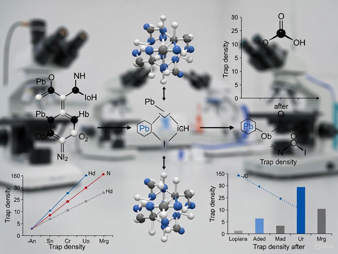
Q1: What is the primary mechanism by which [BMIM]OTF reduces surface defects? A1: [BMIM]OTF acts through a dual coordination mechanism. The OTF⁻ anion has a stronger binding energy (Eb = -1.49 eV) with uncoordinated Pb²⁺ on the QD surface compared to traditional ligands like octanoic acid (Eb = -0.95 eV). Simultaneously, the [BMIM]+ cation coordinates with Br⁻ ions on the surface (Eb = -1.00 eV). This strong dual passivation effectively suppresses the formation of bromide vacancies and Pb-related defects, which are major non-radiative recombination centers [4].
Q2: Can [BMIM]OTF be used for other perovskite formulations beyond CsPbBr3? A2: While the cited research focuses on CsPbBr3 QDs, the fundamental passivation chemistry is likely applicable to other halide compositions (e.g., Cl, I) and mixed-cation perovskites. The key is the interaction between the OTF⁻ anion and the metal lead and the cation with the halides, which is a common feature in lead halide perovskites. However, optimization of concentration and processing conditions would be necessary [4] [38].
Q3: How does [BMIM]OTF enhance the crystallinity of perovskite QDs? A3: During the in-situ synthesis, the positively charged N+ of the [BMIM]+ ion coordinates with Br− ions, forming a complex with the [PbBr3]− octahedron. The imidazole ring also introduces a steric hindrance effect, which slows down the subsequent nucleation process when Cs+ cations combine with the octahedrons. This controlled, delayed nucleation promotes the growth of larger QDs with higher crystallinity, as evidenced by XRD and TEM [4].
Q4: Are there stability improvements associated with using [BMIM]OTF? A4: Yes, the enhanced surface passivation and reduced defect density contribute to improved operational stability. Research reports a significant increase in the T50 operational lifetime from 8.62 hours to 131.87 hours (normalized to an initial brightness of 100 cd/m²) for PeLEDs incorporating [BMIM]OTF-treated QDs [4].
Q5: What are the key characterization techniques to verify the effectiveness of [BMIM]OTF? A5: Essential characterization methods include:
- Transient Photoluminescence (TRPL): To measure the increase in exciton recombination lifetime.
- X-ray Diffraction (XRD): To confirm enhanced crystallinity, particularly of the (200) plane.
- Transmission Electron Microscopy (TEM): To analyze the increase in QD size and uniformity.
- Photoluminescence Quantum Yield (PLQY): To quantify the reduction in non-radiative recombination.
- Electroluminescence (EL) Response Measurement: To directly measure the improvement in device response speed [4].
The table below summarizes key performance metrics achieved with [BMIM]OTF treatment, as reported in the literature, providing benchmarks for your research.
Table 1: Quantitative Performance Enhancement with [BMIM]OTF
| Performance Parameter | Control (Without [BMIM]OTF) | With [BMIM]OTF Optimization | Improvement | Source |
|---|---|---|---|---|
| PLQY (QD Solution) | 85.6% | 97.1% | +11.5% | [4] |
| Average Exciton Lifetime (τavg) | 14.26 ns | 29.84 ns | +109% | [4] |
| EL Response Rise Time | ~2.8 µs (extrapolated) | 700 ns | >75% reduction | [4] [36] |
| Maximum EQE (Standard Device) | 7.57% | 20.94% | ~2.8x increase | [4] |
| Maximum EQE (9072 PPI Device) | Not Reported | 15.79% | - | [4] |
| T50 Operational Lifetime (L₀=100 cd/m²) | 8.62 h | 131.87 h | ~15x increase | [4] |
| Peak Brightness | Not Reported | >170,000 cd/m² | - | [4] [36] |
Detailed Experimental Protocols
Protocol 1: In-situ Synthesis of [BMIM]OTF-Treated CsPbBr3 QDs
This protocol is adapted from the method used to achieve high-performance QDs [4].
Reagents Needed:
- Cesium acetate (C₂H₃CsO₂, 99.0%)
- Lead bromide (PbBr₂, 99.9%)
- 1-Butyl-3-methylimidazolium Trifluoromethanesulfonate ([BMIM]OTF, ≥98%)
- Oleic Acid (OA, 90%)
- Oleylamine (OAm, 80-90%)
- N,N-Dimethylformamide (DMF, 99.5%)
- Chlorobenzene (CB, anhydrous)
Procedure:
- Precursor Preparation: Dissolve PbBr₂ in DMF with standard OA and OAm ligands to create the lead bromide precursor solution.
- Ionic Liquid Addition: Dissolve a calculated amount of [BMIM]OTF in chlorobenzene. This solution is then added to the lead bromide precursor.
- Nucleation and Growth: Inject the cesium acetate precursor into the mixture under stirring. The [BMIM]OTF will modulate the nucleation process.
- Purification: Centrifuge the reaction mixture to isolate the QDs. Wash the pellet with a non-solvent like methyl acetate or toluene to remove unreacted precursors and excess ligands.
- Dispersion: Re-disperse the final QDs in an appropriate solvent like toluene or octane for film deposition.
Key Notes:
- Create a series of samples with varying [BMIM]OTF concentrations (e.g., [BMIM]OTF-1, [BMIM]OTF-2, [BMIM]OTF-3) to identify the optimal concentration for your specific setup [4].
- The entire synthesis should be performed in an inert atmosphere (e.g., nitrogen glovebox).
Protocol 2: Fabrication of Ultra-Fast PeLEDs
This protocol outlines the key steps for fabricating light-emitting diodes with nanosecond response [4] [36].
Key Steps:
- Substrate Preparation: Clean and plasma-treat ITO-coated glass substrates.
- Charge Transport Layers: Deposit hole injection and transport layers (e.g., PEDOT:PSS) via spin-coating and annealing.
- Active Layer Deposition: Spin-coat the synthesized [BMIM]OTF-treated CsPbBr3 QD ink onto the transport layer to form the emissive film.
- Electrode Deposition: Thermally evaporate an electron transport layer (e.g., TPBi), a LiF interlayer, and finally a metal cathode (e.g., Al).
- Patterning for Speed: To achieve the fastest response, define very small active pixel areas (e.g., 1.3 μm pixel size) to minimize device capacitance, which is critical for the nanosecond operation [4].
The Scientist's Toolkit: Research Reagent Solutions
Table 2: Essential Materials for [BMIM]OTF-based Perovskite QD Research
| Reagent / Material | Function / Role | Key Consideration |
|---|---|---|
| [BMIM]OTF | Primary additive for defect passivation & crystallinity enhancement. | Purity (≥98%) is critical. Acts as a crystallization modulator and surface passivator [4]. |
| Lead Bromide (PbBr₂) | Lead and halide source for the perovskite lattice. | High purity (≥99.9%) minimizes intrinsic impurities that act as defects [4]. |
| Cesium Acetate | Cesium source for the APbX₃ structure. | Acetate anion can assist in precursor conversion and may itself act as a ligand [4] [22]. |
| Oleic Acid (OA) / Oleylamine (OAm) | Surface ligands for colloidal stability during synthesis. | Ratio and concentration affect QD growth, stability, and final film conductivity [4]. |
| Chlorobenzene | Solvent for [BMIM]OTF in the in-situ synthesis. | Anhydrous grade is required to prevent premature degradation of precursors [4]. |
| Dimethylformamide (DMF) | Polar solvent for precursor dissolution. | Anhydrous grade is essential for reproducibility and high PLQY [4]. |
Experimental Workflow and Mechanism Visualization
The following diagram illustrates the experimental workflow for synthesizing [BMIM]OTF-treated QDs and fabricating high-speed PeLEDs.
Diagram 1: Experimental workflow for PeLED fabrication.
The next diagram illustrates the proposed mechanism of defect passivation by [BMIM]OTF on the surface of a perovskite quantum dot.
Diagram 2: Mechanism of [BMIM]OTF passivation on QD surface.
Technical FAQs: Fundamental Concepts
Q1: What is a sacrificial layer in the context of perovskite quantum dot films? A sacrificial layer is a temporary material layer applied during fabrication that actively improves the interface quality of the final structure, often by preventing unwanted reactions or by passivating defects, and is sometimes removed or transformed after serving its purpose [39] [40]. In perovskite quantum dot (PQD) research, this strategy is emerging as a method to reduce surface trap density and enhance optoelectronic properties.
Q2: How do sacrificial layers specifically help reduce trap density in PQDs? Sacrificial layers and related interface engineering strategies help reduce trap density by:
- Suppressing Interfacial Reactions: Preventing the formation of defect-inducing layers, such as resistive silicon oxide (SiOx), during high-temperature processing of adjacent layers [39].
- Direct Defect Passivation: Coordinating with unsaturated bonds on the PQD surface, thereby eliminating charge trapping sites that cause non-radiative recombination [4].
- Promoting Favorable Crystallization: Modifying the crystal growth environment to produce larger, higher-quality QDs with a lower surface-area-to-volume ratio, which inherently reduces the number of surface defects [4].
Q3: Can a sacrificial layer be regenerated after its removal? Yes, for some systems, a key advantage is the ability to regenerate the sacrificial layer. Research on thin-film composite membranes has demonstrated that certain sacrificial layers, such as Fe3+-TA (tannic acid complexed with iron ions), can be removed and then re-coated in situ for multiple cycles, restoring performance after scaling or fouling occurs [40].
Troubleshooting Guides: Experimental Challenges
Issue: Incomplete Passivation or Low Film Photoluminescence Quantum Yield (PLQY)
Problem: After applying the passivation strategy, the PQD film shows low PLQY, indicating a high density of non-radiative recombination centers.
Diagnosis and Solutions:
| Possible Cause | Diagnostic Method | Solution |
|---|---|---|
| Insufficient coordination of the passivation agent with the QD surface. | Analyze binding energies via Density Functional Theory (DFT) calculations; perform Fourier-transform infrared spectroscopy (FTIR). | Use passivators with stronger binding energy. For instance, the OTF− anion shows a higher binding energy to Pb²⁺ on QD surfaces (-1.49 eV) than common octanoic acid (-0.95 eV) [4]. |
| High surface area ratio of QDs, making full passivation difficult. | Transmission Electron Microscopy (TEM) for size analysis; statistical size distribution. | Employ additives like ionic liquid [BMIM]OTF to promote the growth of larger QD crystals, thereby reducing the surface area requiring passivation [4]. |
| Severe bulk recombination due to interior defects (e.g., Sn vacancies in Sn-based perovskites). | Thermally Stimulated Current (TSC) measurements to profile trap density and depth. | Incorporate smaller-sized additive ions (e.g., Ge) into the perovskite matrix to reduce bulk trap density and carrier concentration [41]. |
Recommended Workflow:
Issue: Poor Charge Injection and Slow Device Response
Problem: The fabricated PeLEDs or solar cells exhibit a slow rise in electroluminescence response or poor charge extraction, leading to low efficiency.
Diagnosis and Solutions:
| Possible Cause | Diagnostic Method | Solution |
|---|---|---|
| Insulating surface ligands on QDs hindering charge transport. | Time-resolved photoluminescence (TRPL); measure device response time under pulse voltage. | Implement ligand engineering to replace long, insulating ligands with shorter, conductive ones, or use ionic liquids like [BMIM]OTF to improve carrier injection [4]. |
| High injection barrier at the interface between the QD layer and charge transport layer. | Ultraviolet photoelectron spectroscopy (UPS) for energy level alignment; current-density-voltage (J-V) characterization. | Insert an ultrathin organic interfacial layer (e.g., PEDOT:PSS) to tune energy level alignment and facilitate charge transfer via efficient recombination [39]. |
| Massive charge trapping at the interface. | External Quantum Efficiency (EQE) measurement; impedance spectroscopy. | Apply a sacrificial passivation layer that permanently heals interfacial defects, reducing trap-assisted recombination [42] [4]. |
Recommended Workflow:
Research Reagent Solutions
The table below lists key reagents used in advanced interfacial passivation strategies for perovskite quantum dot research.
| Reagent Name | Function / Role | Key Experimental Insight |
|---|---|---|
| PEDOT:PSS (Poly(3,4-ethylenedioxythiophene):polystyrene sulfonate) | Sacrificial Interface Layer: Acts as a temporary layer to prevent resistive SiOx formation during subsequent layer deposition and enables efficient charge recombination [39]. | An ultrathin layer inserted between TCO and HTL restores junction functionality, enabling tandem solar cells with a fill factor up to 81.3% [39]. |
| [BMIM]OTF (1-Butyl-3-methylimidazolium Trifluoromethanesulfonate) | Crystallization Modifier & Defect Passivator: Enhances QD crystallinity, increases QD size, and passivates surface defects via coordination of both cation ([BMIM]+) and anion (OTF−) [4]. | Reduces EL response rise time by over 75% and boosts EQE from 7.57% to 20.94%. OTF− shows stronger binding to Pb²⁺ (-1.49 eV) than common ligands [4]. |
| LiTFSI (Lithium bis(trifluoromethanesulfonyl)imide) | Electron Transport Layer (ETL) Modifier: Passivates oxygen vacancies in SnO₂ ETL and improves energy level alignment with the perovskite layer [42]. | Treatment of SnO₂ ETL with LiTFSI increased PSC efficiency from 18.55% to 20.84% by improving charge extraction and reducing hysteresis [42]. |
| Ge ions (Germanium) | Bulk Additive: Reduces trap density and carrier concentration in tin-based perovskites, effectively passivating deep traps associated with Sn vacancies [41]. | 7.5 mol% Ge doping doubled the reduction of total trap density to 4.14 × 10²⁰ cm⁻³, increasing Voc from 0.36 V to 0.46 V in a tin-based PSC [41]. |
| Fe³⁺-TA Complex (Tannic Acid with Iron Ions) | Regenerable Sacrificial Layer: Forms a removable layer that improves surface smoothness and provides a physical barrier against scaling, which can be regenerated in situ [40]. | Demonstrated excellent anti-scaling performance and durability over six reuse cycles with a flux recovery rate exceeding 97% [40]. |
The following table summarizes quantitative performance improvements achieved by various interfacial and sacrificial layer strategies.
| Material System | Strategy / Reagent | Key Performance Improvement | Reference |
|---|---|---|---|
| Monolithic Perovskite/Si Tandem Solar Cell | Ultrathin PEDOT:PSS sacrificial layer | Power Conversion Efficiency (PCE): 21.95%; Fill Factor (FF): 81.3% (among highest reported) [39]. | [39] |
| Perovskite Solar Cell (SnO₂ ETL) | LiTFSI modification of SnO₂ | PCE: Control 18.55% → Modified 20.84% [42]. | [42] |
| CsPbBr₃ Perovskite QLED | [BMIM]OTF treatment of QDs | EQE: 7.57% → 20.94%; PLQY: 85.6% → 97.1%; Avg. Exciton Lifetime: 14.26 ns → 29.84 ns; EL Response Time: Reduced by >75% [4]. | [4] |
| Tin-based Perovskite Solar Cell | 7.5 mol% Ge additive | Trap Density: Reduced to 4.14 × 10²⁰ cm⁻³ (approx. half of control); PCE: Control 3.96% → Ge-doped 7.45%; Voc: 0.36 V → 0.46 V [41]. | [41] |
| Thin-Film Composite Membrane | Fe³⁺-TA Sacrificial Layer | Flux Recovery: >97% over 6 reuse cycles in gypsum scaling tests [40]. | [40] |
Research Reagent Solutions
The following table details key reagents essential for the optimized synthesis of reproducible, low-trap-density perovskite quantum dots.
| Reagent Name | Function / Role in Synthesis | Key Benefit / Rationale |
|---|---|---|
| Dual-functional Acetate (AcO⁻) | Cesium precursor additive and surface ligand [12] [43] [44]. | Improves cesium salt conversion purity (from ~70% to ~99%), reduces by-products, and passivates surface dangling bonds [12] [44]. |
| 2-Hexyldecanoic Acid (2-HA) | Short-branched-chain ligand [12] [43] [44]. | Stronger binding affinity to QD surface than oleic acid; passivates defects and suppresses Auger recombination [12]. |
| 1-Butyl-3-methylimidazolium Trifluoromethanesulfonate ([BMIM]OTF) | Ionic liquid additive for crystallization control [4]. | Enhances QD crystallinity and size, reduces surface defects and charge injection barriers, leading to higher PLQY and faster device response [4]. |
| Cs-Oleate | Standard cesium precursor. | Baseline reagent; its incomplete conversion and by-product formation are key issues addressed by AcO⁻ [12]. |
Troubleshooting Guide & FAQs
Q1: Our CsPbBr₃ quantum dot synthesis consistently results in low Photoluminescence Quantum Yield (PLQY < 80%) and large batch-to-batch variations. What is the primary cause, and how can we address it?
A1: The primary cause is often the incomplete conversion of the cesium precursor and the formation of by-products, leading to inconsistent nucleation and a high density of surface defects that cause non-radiative recombination [12].
Solution: Optimize your cesium precursor recipe. Incorporate a dual-functional acetate (AcO⁻) ion. This approach has been shown to increase the purity of the cesium precursor from 70.26% to 98.59%, drastically improving homogeneity. The AcO⁻ also acts as a surface ligand to passivate dangling bonds. Combined with a strong-binding ligand like 2-hexyldecanoic acid (2-HA), this method can achieve PLQYs up to 99% with excellent batch-to-batch reproducibility [12] [43] [44].
Q2: We observe a slow rise in electroluminescence (EL) response in our QD-LED devices, which limits their use in high-speed displays. What material property is responsible, and how can we improve the response speed?
A2: The slow EL response is typically due to hindered charge injection and massive charge trapping at the insulating and defective surface of the quantum dots [4].
Solution: Implement surface and interface engineering to reduce defect states and injection barriers. Using an ionic liquid like [BMIM]OTF during synthesis can enhance QD crystallinity, increase particle size, and effectively passivate surface defects via strong coordination. This strategy has been demonstrated to reduce the EL rise time by over 75% and achieve nanosecond-scale response times in devices [4].
Q3: Despite high initial PLQY, our quantum dot films suffer from rapid degradation under ambient conditions. What are the key instability factors, and what stabilization strategies can we employ?
A3: Perovskite QDs are susceptible to degradation from moisture, oxygen, and heat due to structural and interfacial instabilities [45] [15] [46].
Solution: A multi-pronged stabilization approach is recommended:
- Ligand Engineering: Use ligands with stronger binding affinity (e.g., 2-HA) to create a more stable surface [12] [46].
- Compositional Engineering: Dope the QD composition with stabilizing elements [46].
- Matrix Encapsulation: Embed the QDs in a protective polymer or inorganic matrix. For instance, embedding QDs in polymer microspheres during a spray-drying process has been shown to enhance stability for display applications [15] [47].
Detailed Experimental Protocols
Protocol: Synthesis of High-Reproducibility CsPbBr₃ QDs via Acetate-Modified Precursor
This protocol is adapted from the work of Tao et al. [12] [43] [44], which focuses on reducing trap density by improving precursor purity and surface passivation.
Objective: To synthesize CsPbBr₃ QDs with high PLQY (>95%), narrow size distribution, and excellent batch-to-batch reproducibility.
Materials:
- Cesium carbonate (Cs₂CO₃)
- Lead bromide (PbBr₂)
- 1-Octadecene (ODE)
- Oleic acid (OA)
- Oleylamine (OAm)
- Acetic acid (or cesium acetate) - Source of AcO⁻ ions.
- 2-Hexyldecanoic acid (2-HA) - Alternative ligand.
Procedure:
- Cesium Oleate-Acetate Precursor Synthesis:
- Load Cs₂CO₃ (0.2 g), ODE (5 mL), and OA (0.5 mL) into a 25 mL flask.
- Critical Step: Add a controlled amount of acetic acid (e.g., 0.1 mL) to the mixture. This introduces the AcO⁻ ions.
- Dry and degas the mixture under vacuum at 120 °C for 60 minutes.
- Heat the solution under an inert atmosphere (N₂) to 150 °C until all Cs₂CO₃ has reacted and the solution is clear. The inclusion of AcO⁻ ensures a more complete reaction, minimizing unreacted precursor and by-products.
PbBr₂ Precursor Preparation:
- In a separate flask, mix PbBr₂ (0.1 g), ODE (5 mL), OA (0.5 mL), and OAm (0.5 mL).
- Dry and degas under vacuum at 120 °C for 60 minutes.
- Heat to 120-150 °C under N₂ until a clear solution is obtained.
Quantum Dot Synthesis (Hot-Injection):
- Rapidly inject the preheated Cs-oleate-acetate precursor (0.4 mL) into the vigorously stirring PbBr₂ precursor solution at a set temperature (e.g., 170 °C).
- Allow the reaction to proceed for 5-10 seconds.
- Immediately cool the reaction mixture in an ice-water bath to terminate growth.
Ligand Exchange / Post-Synthesis Treatment:
- Critical Step: Precipitate the crude QDs by adding a polar solvent (e.g., methyl acetate) and centrifuge.
- Re-disperse the QD pellet in a non-polar solvent (e.g., hexane or toluene) containing a small amount of 2-hexyldecanoic acid (2-HA). This step replaces the more labile oleic acid ligands, providing a more robust and defect-free surface.
- Repeat the precipitation and re-dispersion cycle to remove excess ligands and by-products.
Expected Outcomes: When successfully executed, this protocol should yield CsPbBr₃ QDs with:
- A green emission peak at ~512 nm.
- A narrow FWHM (Full Width at Half Maximum) of ~22 nm.
- A PLQY consistently above 95%, often reaching 99% [12].
- A significantly reduced Amplified Spontaneous Emission (ASE) threshold (~0.54 μJ·cm⁻²) [12].
The table below quantifies the performance enhancement achieved through the optimized synthesis protocol.
| Performance Parameter | Standard Synthesis (with OA) | Optimized Synthesis (with AcO⁻ & 2-HA) | Improvement | Source |
|---|---|---|---|---|
| Cesium Precursor Purity | 70.26% | 98.59% | ~40% increase | [12] |
| Photoluminescence Quantum Yield (PLQY) | ~85% (Baseline from [4]) | 99% | ~16% increase (absolute) | [12] |
| ASE Threshold | 1.8 μJ·cm⁻² | 0.54 μJ·cm⁻² | 70% reduction | [12] [44] |
| Relative Standard Deviation (Size Distribution) | 9.02% | 0.82% | ~91% reduction (improved uniformity) | [12] |
Experimental Workflow and Mechanism Visualization
High-Reproducibility QD Synthesis Workflow
Ligand Coordination and Defect Passivation Mechanism
Compositional engineering of A-site cations and halide anions is a foundational strategy for enhancing the intrinsic lattice stability of perovskite quantum dots (PQDs). By carefully selecting and mixing ions at the A-site and X-site of the ABX₃ perovskite crystal structure, researchers can directly influence the formation energy of defects, suppress ion migration, and stabilize the desired photoactive crystal phase against environmental stressors such as heat, light, and humidity. This guide addresses key challenges and provides proven methodologies for reducing trap density and improving the operational lifetime of PQD-based devices through targeted compositional design [48] [49].
Frequently Asked Questions (FAQs) & Troubleshooting
1. How does A-site cation composition influence thermal stability and what are the degradation pathways? The choice of A-site cation significantly affects the thermal degradation mechanism of PQDs. Experimental studies, supported by in situ XRD and DFT calculations, reveal two primary pathways dependent on the A-site composition [13]:
- Cs-Rich PQDs (e.g., CsₓFA₁₋ₓPbI₃ with high x): Degradation is typically initiated by a phase transition from the black, photoactive γ-phase to a yellow, non-perovskite δ-phase.
- FA-Rich PQDs (e.g., CsₓFA₁₋ₓPbI₃ with low x): These materials tend to directly decompose into PbI₂ and other byproducts without undergoing a phase transition.
Notably, FA-rich PQDs can exhibit slightly better thermal stability than their all-inorganic CsPbI₃ counterparts, which is correlated with their higher surface ligand binding energy. This stronger ligand binding helps to passivate the surface and resist degradation [13].
2. Why does my perovskite quantum dot film have a high trap state density despite using mixed cations? High trap density in mixed-cation films often originates from uncontrolled cation vacancies and inadequate surface passivation. Cation vacancies, such as V₊, can introduce local lattice distortion, which acts as a non-radiative recombination center, reducing photoluminescence quantum yield (PLQY) and accelerating degradation [50]. Furthermore, during the film deposition process, the loss of native insulating ligands (like oleic acid and oleylamine) without proper replacement with shorter, conductive ligands can leave behind a high density of uncoordinated Pb²⁺ sites and halide vacancies, which are major sources of traps [48] [51].
3. How can I tune the bandgap of my PQDs for specific applications without compromising stability? Halide anion exchange is a highly effective post-synthetic method for bandgap tuning. You can achieve a continuous shift in the emission peak across the entire visible spectrum (e.g., from ~650 nm for CsPbI₃ to ~800 nm for FAPbI₃) by conducting an anion-exchange reaction at room temperature using PbX₂ and alkylammonium halides as halide sources [48]. The organic ligand shell on PQDs acts as a barrier against halide migration, which helps to alleviate the halide segregation issues common in bulk perovskite films, thereby maintaining stability after tuning [48].
4. My PQD films lose photoluminescence after deposition. What is the primary cause? The significant drop in PL after film formation is primarily due to defect regeneration during the solvent evaporation and film assembly process. This leads to the loss of surface ligands and the creation of dangling bonds, which become non-radiative recombination centers [51]. Implementing a bilateral interfacial passivation strategy, where both the top and bottom interfaces of the PQD film are treated with suitable molecules (e.g., phosphine oxide-based ligands like TSPO1), can effectively passivate these regenerated defects and restore high PLQY [51].
Key Experimental Protocols
Hot-Injection Synthesis of CsPbBr₃ Quantum Dots
This is a standard method for producing high-quality, monodisperse PQDs with excellent size control [48] [51].
- Materials: Cs₂CO₃, PbBr₂, 1-Octadecene (ODE), Oleic Acid (OA), Oleylamine (OAm).
- Procedure:
- Cs-oleate precursor: Load 0.4 g of Cs₂CO₃, 1.25 mL of OA, and 15 mL of ODE into a 50 mL 3-neck flask. Dry and degas under vacuum at 120 °C for 1 hour, then heat under N₂ to 150 °C until all Cs₂CO₃ reacts.
- Pb precursor: In a separate 100 mL 3-neck flask, load 0.138 g of PbBr₂, 1 mL of OA, 1 mL of OAm, and 10 mL of ODE. Dry under vacuum at 120 °C for 1 hour.
- Injection: Under N₂ atmosphere, raise the temperature of the Pb precursor flask to 160 °C. Quickly inject the preheated Cs-oleate solution (0.8 mL) and stir for 5 seconds.
- Cooling: Immediately cool the reaction mixture using an ice-water bath to terminate the reaction.
- Purification: Centrifuge the crude solution at high speed (e.g., 12,000 rpm for 10 min). Discard the supernatant and redisperse the pellet in a non-polar solvent like hexane. Repeat this centrifugation and redispersion cycle at least twice to remove unreacted precursors and excess ligands [48].
Post-Synthetic Anion-Exchange for Bandgap Tuning
This protocol allows for precise tuning of the emission wavelength after the initial synthesis [48].
- Materials: Purified PQDs (e.g., CsPbBr₃), PbX₂ (X = Cl, I), alkylammonium halide (e.g., Oleylammonium Iodide).
- Procedure:
- Prepare separate solutions of the halide sources (e.g., PbI₂ and Oleylammonium Iodide) in a suitable solvent.
- Mix the purified PQD colloid with the halide source solutions at room temperature.
- The halide ions will travel between the PQD cores and the halide sources in the liquid medium, gradually changing the composition.
- Monitor the reaction progress using UV-Vis absorption and photoluminescence spectroscopy.
- Once the desired optical properties are achieved, purify the QDs again via centrifugation to remove the spent halide sources.
Bilateral Interfacial Passivation for PQD Films
This method drastically reduces interfacial defects in solid-state films, crucial for high-performance devices [51].
- Materials: Spin-coated PQD film, passivation molecules (e.g., TSPO1), organic solvents.
- Procedure:
- Bottom Interface Passivation: Before depositing the PQD film, evaporate a thin layer (~ 5 nm) of the passivation molecule (e.g., TSPO1) onto the underlying charge transport layer.
- PQD Film Deposition: Spin-coat the purified and concentrated PQD ink onto the passivated substrate to form the active film.
- Top Interface Passivation: After PQD film deposition, evaporate another layer of the passivation molecule on top of the PQD film.
- This bilateral passivation creates a strong interaction (e.g., between P=O groups and uncoordinated Pb²⁺) at both interfaces, effectively suppressing defect states and non-radiative recombination.
Quantitative Data for Composition and Property Management
The tables below summarize key quantitative relationships to guide your compositional engineering efforts.
Table 1: A-Site Cation Composition vs. Material Properties in CsₓFA₁₋ₓPbI₃ PQDs
| A-Site Composition | Primary Thermal Degradation Pathway | Ligand Binding Energy (Relative) | Electron-LO Phonon Coupling | Typical PLQY |
|---|---|---|---|---|
| Cs-Rich (high x) | Phase transition (γ- to δ-phase) [13] | Lower [13] | Weaker [13] | Lower [13] |
| FA-Rich (low x) | Direct decomposition to PbI₂ [13] | Higher [13] | Stronger [13] | Higher [13] |
Table 2: Impact of Defects and Passivation on PQD Film Performance
| Parameter | High Trap-State Film (Unpassivated) | Bilateral-Passivated Film |
|---|---|---|
| Film PLQY | ~43% [51] | Up to ~79% [51] |
| LED Current Efficiency | ~20 cd A⁻¹ [51] | ~75 cd A⁻¹ [51] |
| LED EQE (Max) | ~7.7% [51] | ~18.7% [51] |
| Operational Lifetime (T₅₀) | ~0.8 hours [51] | ~15.8 hours [51] |
Experimental Workflow and Defect Passivation Visualization
The following diagrams illustrate the core experimental workflow for creating stable PQDs and the mechanism of defect passivation.
Diagram 1: Experimental workflow for stable perovskite quantum dot film fabrication, highlighting key stability factors at each stage.
Diagram 2: Defect passivation mechanism. Unpassivated films have trap states that quench excitons. Bilateral passivation with ligands (e.g., TSPO1) coordinates with uncoordinated Pb²⁺ sites, removing traps and enabling efficient exciton recombination and transport.
The Scientist's Toolkit: Essential Research Reagents
Table 3: Key Reagents for Compositional Engineering and Passivation
| Reagent Category | Example Compounds | Primary Function in PQD Research |
|---|---|---|
| A-Site Cation Precursors | Cs₂CO₃, FAI (Formamidinium Iodide), MAI (Methylammonium Iodide) [48] [13] | To incorporate inorganic (Cs⁺) or organic (FA⁺, MA⁺) A-site cations, influencing lattice stability, bandgap, and thermal degradation pathways. |
| Halide Anion Precursors | PbBr₂, PbI₂, Alkylammonium Halides (e.g., Oleylammonium Iodide) [48] | To set the initial halide composition and enable post-synthetic anion-exchange for precise bandgap tuning across the visible spectrum. |
| Surface Ligands (Long-Chain) | Oleic Acid (OA), Oleylamine (OAm) [48] [13] | To control nanocrystal growth during synthesis, provide colloidal stability, and initially passivate surface defects. |
| Passivation Molecules (Short-Chain) | TSPO1, DDAB [51] | To replace native long-chain ligands in solid-state films, enhance charge transport, and passivate interfacial defects (e.g., via P=O bonding with Pb²⁺). |
Optimizing Performance and Stability: Troubleshooting Common Pitfalls in Device Fabrication
Frequently Asked Questions (FAQs)
Q1: What is "efficiency roll-off" in perovskite quantum dot (QD) devices? Efficiency roll-off refers to the drop in a device's external quantum efficiency (EQE) as the operating current density or brightness increases. This is a critical issue in both light-emitting diodes (LEDs) and solar cells, as it limits the practical brightness and stability of the device.
Q2: What are the primary causes of efficiency roll-off? The main causes are unbalanced injection of electrons and holes, and the presence of defect states (traps) within the quantum dot film [52] [29]. When charge injection is unbalanced, one type of carrier floods the QDs, leading to increased non-radiative recombination processes like Auger recombination [52]. Simultaneously, trap states at the QD surface or interfaces act as recombination centers, further reducing efficiency [29] [53].
Q3: How does trap density relate to charge injection balance? High trap density directly exacerbates charge injection imbalance. Trap states can capture one type of charge carrier, effectively blocking its transport and creating a buildup of charge [24] [29]. This buildup leads to increased interfacial charge accumulation and recombination losses, which diminishes open-circuit voltage (Voc) and fill factor (FF) in solar cells, and causes efficiency roll-off in LEDs [24].
Q4: What strategies can mitigate unbalanced charge injection? Key strategies include:
- Interface Engineering: Introducing an interlayer (e.g., 2D-MoS₂) at the perovskite/charge transport layer interface to improve energy level alignment and facilitate prompt charge extraction [24].
- Ligand and Crystallinity Control: Using specific ionic liquids or surface treatments to enhance QD crystallinity, reduce surface defects, and improve carrier injection at the interfaces [53].
- Transport Layer Doping: Modifying charge transport layers (e.g., Mg²⁺ doping in ZnO) to tune their carrier mobility to better match the counter electrode [52].
- Device Architecture Design: Creating internal heterojunctions within the QD film to actively separate charges and improve carrier harvesting [54].
Q5: Why is achieving balanced charge injection particularly challenging in QD LEDs (QLEDs)? Hole injection is inherently less efficient than electron injection in many QD systems due to the deep-lying valence levels of the QDs (e.g., in CdSe and InP) and the resulting large energy offset with the work function of the common anode materials [55]. This intrinsic imbalance makes fine-tuning the hole transport pathway paramount.
Troubleshooting Guide: Common Experimental Issues & Solutions
The following table outlines common problems encountered during device fabrication, their potential causes, and verified solutions.
Table 1: Troubleshooting Guide for Charge Injection and Efficiency Roll-off
| Symptom | Potential Cause | Diagnostic Method | Solution |
|---|---|---|---|
| Severe efficiency roll-off at high brightness | Unbalanced electron/hole injection; Auger recombination [52] | Measure J-V-L characteristics; transient electroluminescence (TREL) | Optimize thickness of hole transport layer (HTL); dope electron transport layer (ETL) with Mg²⁺ to reduce electron mobility and match hole injection [52] |
| Low open-circuit voltage (Voc) and fill factor (FF) | High trap density; interfacial charge accumulation; energetic misalignment [24] [29] | Transient photovoltage (TPV); impedance spectroscopy | Insert a 2D material (e.g., MoS₂) interlayer at the perovskite/HTM interface to reduce trap density and improve band alignment [24] |
| Slow electroluminescence (EL) response time | Hindered charge injection; massive charge trapping due to defective QD surface [53] | Time-resolved EL rise measurement; transient photoluminescence (TRPL) | Treat QDs with ionic liquids (e.g., [BMIM]OTF) to enhance crystallinity, reduce surface defects, and lower injection barrier [53] |
| Poor device stability and rapid degradation | Ionic migration; moisture corrosion accelerated by hygroscopic dopants in HTL [24] | Aging tests under ambient/operational conditions; SEM imaging | Use dopant-free polymeric hole transport materials supported by a 2D-MoS₂ interlayer for improved moisture stability [24] |
| Insufficient hole injection into QDs | Deep valence levels of QDs; large energy offset with anode [55] | Cyclic voltammetry; operando photoluminescence measurements | Explore electrochemical doping via electrical double layers (EDLs) in a light-emitting electrochemical cell (LEC) structure to eliminate injection barriers [55] |
The table below consolidates key performance metrics achieved by various charge-balancing strategies reported in the literature.
Table 2: Performance Summary of Charge-Balancing Strategies
| Strategy / Material System | Device Type | Key Performance Improvement | Reference |
|---|---|---|---|
| Mg²⁺ doped ZnO (MZO) ETL + Organic HTL | QLED | EQE of 21.10%; <20% EQE roll-off from 100 to 30,000 cd m⁻² [52] | [52] |
| 2D-MoS₂ at Perovskite/HTM Interface | Dopant-free PSC | PCE of 18.54% (vs. 15.05% control); upgraded Voc and FF; improved stability [24] | [24] |
| Internal CsPbI₃/CsFAPbI₃ Heterojunction | QD Solar Cell | PCE of 15.52% from stabilized power output; improved Jsc from better carrier harvesting [54] | [54] |
| [BMIM]OTF-treated Perovskite QDs | PeLED | EQE from 7.57% to 20.94%; Rise time reduced by >75%; T50 lifetime from 8.62 h to 131.87 h [53] | [53] |
Detailed Experimental Protocols
Protocol 1: Incorporating a 2D-MoS₂ Interlayer for Reduced Trap Density
This protocol is based on the method described by Hemasiri et al. [24].
- Objective: To reduce trap density and mitigate interfacial losses at the perovskite/hole transport material (HTM) interface.
- Synthesis of 2D-MoS₂:
- Intercalation: Perform lithium (Li+) intercalation into bulk MoS₂ powder using butyl lithium in hexane.
- Exfoliation: Subject the intercalated MoS₂ to liquid-phase exfoliation (LPE) via ultrasonication in isopropanol (IPA) to produce stable, few-layer MoS₂ sheets.
- Characterization: Confirm the presence of both metallic (1T) and semiconducting (2H) phases via Raman spectroscopy and AFM.
- Device Fabrication:
- Deposit the electron transport layer (e.g., TiO₂) on the cleaned substrate.
- Spin-coat the triple-cation perovskite (CsFAMA) precursor solution and anneal to form the light-absorbing layer.
- Critical Step: Spin-coat the exfoliated 2D-MoS₂ dispersion onto the perovskite layer to form the interlayer.
- Deposit the dopant-free hole transport layer (e.g., PTAA).
- Complete the device by thermal evaporation of metal contacts (e.g., Au).
- Validation: Compare the trap density and charge recombination kinetics of devices with and without the MoS₂ interlayer using techniques like space-charge-limited current (SCLC) measurements and transient absorption spectroscopy.
Protocol 2: Balancing Charge Injection in QLEDs via Transport Layer Engineering
This protocol is adapted from the work on high-efficiency QLEDs [52].
- Objective: To achieve balanced charge injection by optimizing the charge transport layers.
- Hole Transport Layer (HTL) Optimization:
- Test various organic HTLs (e.g., TFB, Poly-TPD) with different thicknesses.
- Measure the hole mobility of each HTL configuration to establish a baseline.
- Electron Transport Layer (ETL) Tuning:
- Doping: Prepare a solution of ZnO nanoparticles and dope them with Mg²⁺ (e.g., Zn₁₋ₓMgₓO, MZO) by adding a magnesium salt precursor during synthesis.
- Characterization: Confirm doping via XRD and measure the electron mobility of the MZO film. The goal is to lower the electron mobility to match the slower hole mobility of the HTL [52].
- Device Integration & Testing:
- Fabricate QLEDs with the structure: ITO/HTL (optimized)/QD Layer/ETL (MZO)/Cathode.
- Measure the current density-voltage-luminance (J-V-L) characteristics.
- Key Metric: Analyze the external quantum efficiency (EQE) as a function of luminance. A low EQE roll-off indicates successful charge balance.
The Scientist's Toolkit: Essential Research Reagents & Materials
Table 3: Key Reagents for Charge Injection and Trap Reduction Studies
| Reagent / Material | Function | Application Note |
|---|---|---|
| 2D-MoS₂ (Li+ intercalated) | Hole extraction interlayer; reduces trap density and improves energy level alignment at interfaces [24]. | The mixture of 1T and 2H phases influences performance; post-heating can cause phase transformation. |
| Mg²⁺-doped ZnO (MZO) | Electron transport layer; reduced electron mobility helps balance charge injection in LEDs [52]. | Doping concentration must be optimized to precisely tune electron mobility without compromising conductivity. |
| Ionic Liquid [BMIM]OTF | Additive for perovskite QD synthesis; enhances crystallinity, reduces surface defects, and lowers injection barrier [53]. | Slows nucleation, leading to larger QD size and lower surface area, which requires less ligand passivation. |
| Dopant-free PTAA | Polymer-based hole transport material; improves device stability by eliminating hygroscopic dopants [24]. | Often used in conjunction with interlayer materials (e.g., MoS₂) to achieve high performance. |
| LiCF₃SO₃ in PEO | Electrolyte for quantum dot light-emitting electrochemical cells (QLECs); forms electrical double layers to eliminate injection barriers [55]. | Used in simple device architectures to study fundamental charge injection, though hole injection remains a challenge. |
Signaling Pathways and Workflow Diagrams
Diagram Title: Diagnostic and Mitigation Pathway for Efficiency Roll-Off
Diagram Title: Device Architecture for Balanced Charge Injection
Frequently Asked Questions (FAQs) and Troubleshooting Guide
This section addresses common challenges researchers face when working with perovskite quantum dot (PQD) films and provides targeted, evidence-based solutions to enhance their operational stability.
FAQ 1: Why do my perovskite quantum dot films rapidly degrade and lose photoluminescence when exposed to ambient humidity?
- Problem: Your PQD films are likely suffering from water-induced degradation, a common issue due to the ionic nature and surface susceptibility of perovskites.
- Solution: Implement a robust encapsulation or surface passivation strategy.
- Inorganic Matrix Encapsulation: Support CsPbBr₃ QDs on the surface of inorganic materials like hydroxyapatite (HAP). The chemical interaction between the QDs and the HAP support, originating from the occupation of Br vacancies by surface –O⁻ groups, can provide water-resistant properties. This approach has been shown to allow bright green fluorescence in water for over 75 days [56].
- Atomic Layer Deposition (ALD): Encapsulate PQD films with a thin, conformal layer of Al₂O₃. This inorganic coating acts as a robust barrier against moisture infiltration and oxidation. Studies on FAPbBr₃ QDs treated with ALD showed excellent reliability in long-term light aging and temperature/humidity tests (60°C/90% RH) [57].
- Polymer/SiO₂ Hybrid Encapsulation: Embed QDs within a hybrid structure, such as multiple QDs within a SiO₂ matrix (MQD), and then further incorporate them into a polymer film like ethylene-vinyl acetate (EVA). This dual-layer protection significantly improves water resistance and overall film stability [58].
FAQ 2: How can I prevent my PQD films from degrading and aggregating under thermal stress, such as during device operation?
- Problem: Thermal stress causes ligand desorption, phase transition, and eventual decomposition of the perovskite structure.
- Solution: The strategy depends on the A-site cation composition and requires strengthening ligand binding.
- Understand Composition-Dependent Behavior: Recognize that thermal degradation mechanisms vary. Cs-rich PQDs (e.g., CsPbI₃) typically degrade via a phase transition from a black γ-phase to a yellow δ-phase. In contrast, FA-rich PQDs (e.g., FAPbI₃) with higher ligand binding energy directly decompose into PbI₂ at elevated temperatures [13] [59].
- Utilize Inorganic Supports for High-Temperature Stability: Localizing CsPbBr₃ QDs on a hydroxyapatite (HAP) support can create sintering-resistant films. This method stabilizes the QDs, maintaining a particle size of ~2.2 nm even after calcination at 400°C [56].
- Employ Conductive Ligand Capping via Alkaline Treatment: Use an alkali-augmented antisolvent hydrolysis (AAAH) strategy. Treating PQD films with an antisolvent like methyl benzoate (MeBz) in an alkaline environment (e.g., with KOH) facilitates the rapid substitution of pristine insulating oleate ligands with hydrolyzed conductive counterparts. This results in a denser, more conductive, and thermally stable capping layer [60].
FAQ 3: My PQD-based light-emitting diode (PeLED) shows slow response speed and poor efficiency. How can I improve its electrical performance and stability?
- Problem: Slow electroluminescence (EL) response and low efficiency are often caused by hindered charge injection, massive charge trapping at defective surfaces, and ion migration.
- Solution: Focus on surface and interface engineering to reduce trap states and improve charge injection.
- Defect Passivation with Ionic Liquids: Treat PQDs with an ionic liquid like 1-Butyl-3-methylimidazolium Trifluoromethanesulfonate ([BMIM]OTF). This enhances crystallinity, reduces the surface area ratio, and effectively passivates surface defects. This treatment has been shown to reduce the rise time of EL response by over 75% and increase the external quantum efficiency (EQE) from 7.57% to 20.94% [4].
- Ligand Engineering for Enhanced Charge Transport: Replace long-chain insulating ligands (e.g., oleate) with shorter, conductive ones. The AAAH strategy, for example, can double the amount of conductive ligands on the QD surface, leading to fewer trap-states, suppressed trap-assisted recombination, and more efficient charge transport in devices like solar cells [60].
Experimental Protocols for Enhanced Stability
This section provides detailed methodologies for key experiments cited in the FAQs, enabling researchers to replicate these stabilization techniques.
- Objective: To synthesize sintering- and water-resistant perovskite QDs via interaction with an inorganic support.
- Materials: Hydroxyapatite (HAP) crystals, Cesium bromide (CsBr, 99%), Lead bromide (PbBr₂, 99%), N,N-Dimethylformamide (DMF, 99.9%), Cetyltrimethylammonium bromide (CTAB, 99%).
- Procedure:
- Synthesis of CsPbBr₃ QDs: Prepare CsPbBr₃ QDs in DMF solution using standard synthetic methods.
- Supporting QDs on HAP: Introduce HAP crystals into the DMF solution containing CsPbBr₃ QDs. Stir the mixture vigorously at room temperature (24 °C).
- Isolation: Obtain the deep yellow CsPbBr₃/HAP powder by filtration and drying at 60 °C.
- Water-Resistant Shell Formation: Decorate the supported CsPbBr₃ QDs with CTAB to facilitate the formation of a protective CsPb₂Br₅ shell, resulting in the final CsPbBr₃@CsPb₂Br₅/HAP composite.
- Key Characterization:
- Photoluminescence (PL) Intensity: The PL intensity of the supported QDs can be enhanced by about 150 times compared to pristine QDs.
- Stability Test: Monitor PL intensity while immersing the composite in water to confirm stability for over 75 days.
- Thermal Stability: Subject the powder to high-temperature calcination (e.g., 400 °C) and use TEM to confirm that the QD particle size remains stable at ~2.2 nm.
- Objective: To enhance the crystallinity and reduce defect states of PQDs for faster and more efficient light-emitting diodes.
- Materials: Lead bromide precursor, Ionic liquid [BMIM]OTF, Chlorobenzene (CB).
- Procedure:
- In-situ Crystallization: Add [BMIM]OTF dissolved in chlorobenzene to the lead bromide precursor solution to control the nucleation process.
- QD Synthesis: Proceed with the standard synthesis of CsPbBr₃ QDs. The presence of [BMIM]OTF during nucleation will slow the process, promoting the growth of larger, more crystalline QDs.
- Device Fabrication: Integrate the treated QDs into a standard PeLED device architecture, ensuring a small light-emitting unit area to reduce capacitance effects.
- Key Characterization:
- Transmission Electron Microscopy (TEM): Confirm the increase in average QD size (e.g., from 8.84 nm to 11.34 nm).
- Time-Resolved Photoluminescence (TRPL): Measure the exciton recombination lifetime (τavg), which should increase significantly (e.g., from 14.26 ns to 29.84 ns), indicating reduced trap density.
- Device Performance: Measure the EL response time, targeting nanosecond-scale rise times under steady-state operation. Record the EQE, which can exceed 15% for high-resolution devices.
- Objective: To achieve a dense capping of conductive ligands on the PQD surface for superior charge transport.
- Materials: Methyl benzoate (MeBz) antisolvent, Potassium hydroxide (KOH), Hybrid FA₀.₄₇Cs₀.₅₃PbI₃ PQD solid films.
- Procedure:
- Prepare Alkaline Antisolvent: Carefully add a regulated amount of KOH to the MeBz antisolvent to create an alkaline environment.
- Layer-by-Layer Rinsing: During the layer-by-layer deposition of the PQD solid film, rinse each layer with the alkaline MeBz antisolvent.
- Post-treatment: After achieving the desired film thickness, perform a standard post-treatment with short cationic ligands (e.g., FAI or PAI) to complete the surface engineering.
- Key Characterization:
- FTIR/XPS: Verify the substitution of long-chain oleate ligands with hydrolyzed short ligands.
- Solar Cell Performance: Fabricate solar cells to validate the effectiveness. A certified power conversion efficiency (PCE) of 18.3% has been achieved using this method.
- Trap-State Density: Use techniques like space-charge-limited current (SCLC) measurements to confirm a significant reduction in trap-state density in the treated films.
The following tables consolidate key performance metrics from the cited stabilization strategies for easy comparison.
Table 1: Performance Metrics of Moisture Stabilization Strategies
| Stabilization Strategy | Material System | Key Performance Metric | Stability Outcome |
|---|---|---|---|
| Inorganic Support [56] | CsPbBr₃@CsPb₂Br₅/HAP | Photoluminescence (PL) Intensity | ~150x enhancement; stable in water for >75 days |
| ALD Encapsulation [57] | Al₂O₃-coated FAPbBr₃ QDs | Reliability Test | Stable in temp/humidity tests (60°C/90% RH) |
| Polymer/SiO₂ Hybrid [58] | CdSe/ZnS QDs in MQD/EVA film | PL Quenching under high exposure | 19% quenching vs. 48% in bare QDs |
Table 2: Performance Metrics of Thermal & Electrical Stabilization Strategies
| Stabilization Strategy | Material System | Key Performance Metric | Result |
|---|---|---|---|
| Ionic Liquid Treatment [4] | [BMIM]OTF-treated CsPbBr₃ QDs | EL Response Time / EQE | Reduced by >75% / Up to 20.94% |
| Alkaline Antisolvent [60] | KOH/MeBz-treated Hybrid PQDs | Solar Cell PCE / Ligand Quantity | Certified 18.3% / ~2x conventional amount |
| A-site Cation Engineering [13] | CsₓFA₁₋ₓPbI₃ PQDs | Ligand Binding Energy | FA-rich QDs have higher binding energy |
Research Reagent Solutions
This table lists essential materials and their functions for implementing the described stability strategies.
Table 3: Key Reagents for Enhancing PQD Stability
| Reagent | Function / Role in Stabilization | Application Context |
|---|---|---|
| Hydroxyapatite (HAP) | Inorganic support material; interacts with QD surface to inhibit sintering and enhance PL [56]. | Thermal & Water Stability |
| 1-Butyl-3-methylimidazolium Trifluoromethanesulfonate ([BMIM]OTF) | Ionic liquid for surface passivation; enhances crystallinity and reduces defect states [4]. | Electrical Performance (Reducing Trap Density) |
| Methyl Benzoate (MeBz) with KOH | Alkaline antisolvent system for hydrolyzing and substituting insulating ligands with conductive ones [60]. | Charge Transport & Stability |
| Trimethylaluminum (TMA) & O₃ | Precursors for Atomic Layer Deposition (ALD) of Al₂O₃ encapsulation layers [57]. | Moisture & Environmental Encapsulation |
| Cetyltrimethylammonium Bromide (CTAB) | Surface-active agent to decorate QDs and facilitate formation of a protective CsPb₂Br₅ shell [56]. | Water-Resistant Shell Formation |
Workflow and Strategy Diagrams
The following diagram illustrates the logical decision process for selecting the appropriate stabilization strategy based on the primary stressor affecting the perovskite quantum dot film.
Stabilization Strategy Selection Flow
In the pursuit of high-performance perovskite quantum dot (QD) light-emitting diodes (PeLEDs), managing non-radiative recombination losses at high current densities remains a critical challenge. Auger recombination, a three-carrier non-radiative process, becomes particularly dominant under high excitation, leading to efficiency roll-off and limited device stability. This technical support document outlines the fundamental mechanisms and presents practical ligand-based strategies to suppress these losses, directly supporting broader research objectives in reducing trap density in perovskite QD films.
Understanding Auger Recombination: Core Concepts for Researchers
What is Auger Recombination and Why Does it Limit My Device Performance?
Auger recombination is a non-radiative process where the energy released from an electron-hole recombination event is transferred to a third charge carrier (a second electron or a second hole) instead of being emitted as a photon [61] [62]. This excited carrier then relaxes to the band edge by releasing its energy as heat through collisions with the lattice [61]. The rate of Auger recombination is proportional to the cube of the carrier density (n³ or p³), making it particularly detrimental at the high current densities required for bright electroluminescence [61] [63]. In practical terms, this manifests as efficiency roll-off, where your device's external quantum efficiency (EQE) peaks at a low current density and then drops significantly as you drive the device harder to achieve higher brightness [63].
How is Auger Recombination Different from Other Recombination Pathways?
It is crucial to distinguish Auger recombination from other common loss mechanisms to diagnose and address the correct problem. The table below summarizes the key characteristics of the primary recombination pathways in perovskite quantum dots.
Table 1: Key Recombination Pathways in Perovskite Quantum Dots
| Recombination Type | Process Description | Carriers Involved | Radiative/ Non-Radiative | Rate Dependency |
|---|---|---|---|---|
| Auger | Energy from e-h recombination excites a third carrier [61] [64]. | Three (e.g., two electrons & one hole) | Non-radiative | ∝ n³ or p³ (High carrier density) |
| Shockley-Read-Hall (SRH) | Trap-assisted recombination via defect states in the bandgap [3] [64]. | One carrier at a time | Typically Non-radiative | ∝ n or p (Trap density) |
| Radiative (Bimolecular) | Direct band-to-band recombination emitting a photon [3] [64]. | One electron and one hole | Radiative | ∝ n p |
Troubleshooting Guide: FAQs on Suppressing Auger Losses
FAQ: My PeLEDs show a severe efficiency roll-off at high currents. Is this definitely caused by Auger recombination?
While efficiency roll-off can have multiple contributors, a sharp decline in efficiency at high current densities is a classic signature of dominant Auger recombination [63]. You can confirm this by analyzing your device's recombination kinetics. A recombination rate that scales with the cube of the carrier density (e.g., from power-dependent photoluminescence measurements) is a strong indicator of a significant Auger process [61]. Furthermore, in quasi-2D perovskites, a high exciton binding energy (E₆) strongly correlates with accelerated Auger recombination due to enhanced electron-hole interaction, making this system particularly susceptible [63].
FAQ: How can ligand engineering specifically suppress Auger recombination?
Ligand strategies can suppress Auger recombination through two primary, interconnected mechanisms that reduce the cube of the carrier density and the fundamental Auger coefficient:
- Reducing Exciton Binding Energy (E₆): Introducing polar organic cations can weaken the dielectric confinement in quasi-2D perovskites. For example, replacing phenethylammonium (PEA⁺) with p-fluorophenethylammonium (p-FPEA⁺), which has a higher dipole moment, was shown to reduce E₆ from 347 meV to 211 meV. This reduction led to a more than one-order-of-magnitude decrease in the Auger recombination rate constant [63].
- Decreasing Defect-Assisted Auger Initiation: Defects can act as initiation sites for Auger processes. A dual-ligand synergistic passivation engineering (DLSPE) strategy can simultaneously address bulk and surface defects. For instance, using europium acetylacetonate (Eu(acac)₃) to passivate internal Pb²⁺ vacancies and benzamide to passivate under-coordinated surface halide ions can drastically reduce defect density, thereby suppressing defect-mediated pathways that lead to Auger losses [65].
FAQ: I passivated my QDs, but my response time is still slow. Are these issues related?
Yes, they are intrinsically linked. A slow electroluminescence (EL) response time often indicates persistent trap states and hindered charge injection, which can lead to carrier accumulation and increased probability of Auger recombination at high speeds [4]. Enhancing passivation and improving injection can address both issues. Research shows that using an ionic liquid like 1-Butyl-3-methylimidazolium Trifluoromethanesulfonate ([BMIM]OTF) can enhance QD crystallinity, reduce surface defects, and lower the charge injection barrier. This approach has been demonstrated to reduce the EL rise time by over 75% while simultaneously boosting the external quantum efficiency (EQE), as effective passivation reduces traps that cause both non-radiative losses and slow response [4].
Experimental Protocols & Workflows
Protocol: Dual-Ligand Synergistic Passivation for QDs
This protocol is adapted from a study that achieved a near-unity PLQY of 98.56% and significantly suppressed non-radiative decay [65].
- Objective: To simultaneously passivate bulk and surface defects in CsPbBr₃ QDs using a dual-ligand system.
- Materials:
- Cs₂CO₃, PbBr₂, Oleic Acid (OTAc), Oleylamine (OAm), Tetraoctylammonium bromide (TOAB), Europium acetylacetonate (Eu(acac)₃), Benzamide, Non-polar solvents (e.g., octane, hexane).
- Procedure:
- Cs Precursor Synthesis: Load Cs₂CO₃ and OTAc into a vial. Stir at room temperature until completely dissolved [65].
- QD Synthesis with Bulk Passivation:
- Dissolve PbBr₂, TOAB, and a controlled molar ratio of Eu(acac)₃ (e.g., 0.2 mmol per 1 mmol PbBr₂) in a non-polar solvent [65].
- Under inert atmosphere and stirring, swiftly inject the Cs-precursor into the PbBr2/Eu(acac)₃ solution.
- Allow the reaction to proceed for a few seconds before cooling in an ice bath.
- Surface Ligand Exchange:
- Precipitate the crude solution with a polar anti-solvent (e.g., methyl acetate) and centrifuge.
- Re-disperse the pellet in a solvent containing benzamide (e.g., 0.5 mg/mL).
- Stir for a period to allow ligand exchange, then precipitate and re-disperse in a desired solvent for film formation [65].
- Validation: Characterize success via HR-XRD for phase purity, FT-IR for surface chemistry, and measure PLQY and transient PL lifetime to quantify reduction in non-radiative recombination [65].
Workflow: Rational Ligand Selection for Auger Suppression
The following diagram illustrates a logical workflow for selecting and testing ligand strategies to manage Auger recombination.
The Scientist's Toolkit: Key Research Reagents
The table below catalogs essential reagents discussed for managing Auger and non-radiative losses.
Table 2: Key Reagents for Suppressing Non-Radiative Recombination
| Reagent / Material | Function / Role | Key Experimental Consideration |
|---|---|---|
| p-Fluorophenethylammonium (p-FPEA⁺) | Polar organic cation that reduces dielectric confinement and exciton binding energy, directly suppressing the Auger coefficient [63]. | The electron-withdrawing fluorine atom creates a strong molecular dipole. Optimal concentration in precursor solution must be determined. |
| Europium Acetylacetonate (Eu(acac)₃) | Bulk passivator; Trivalent Eu³⁺ ions compensate for positively charged Pb²⁺ vacancies, while acac coordinates with surface halides [65]. | Acts as a dopant. Molar ratio relative to Pb²⁺ is critical (e.g., 0.2 mmol per 1 mmol PbBr₂) to avoid altering crystal structure [65]. |
| Benzamide | Short-chain surface passivator; Electron-rich amide groups coordinate with under-coordinated Br⁻ ions on the QD surface [65]. | Its short conjugated backbone reduces steric hindrance, improving charge transport. Used in post-synthesis ligand exchange [65]. |
| 1-Butyl-3-methylimidazolium Trifluoromethanesulfonate ([BMIM]OTF) | Ionic liquid additive that enhances QD crystallinity, reduces surface defects, and lowers charge injection barriers [4]. | Added in-situ during QD synthesis. Improves PLQY and device response speed. Concentration needs optimization to prevent aggregation [4]. |
| Oleic Acid / Oleylamine | Standard long-chain ligands for colloidal QD synthesis and stabilization [65]. | Provide initial stability but can hinder charge transport. Often partially replaced by short-chain ligands in high-performance devices [65]. |
This technical support guide provides targeted troubleshooting for researchers aiming to reduce trap density in perovskite quantum dot (QD) films. Controlling film morphology is critical for minimizing inter-grain recombination, as defects at grain boundaries and non-uniform surfaces act as charge traps that quench photoluminescence and degrade device performance. The following sections address specific experimental challenges and provide detailed protocols to achieve optimal results.
Troubleshooting FAQs: Common Experimental Challenges
1. My perovskite QD films have low photoluminescence quantum yield (PLQY). How can I reduce non-radiative recombination?
Issue: Low PLQY typically indicates a high density of surface defects and traps that promote non-radiative recombination, often caused by poor QD surface passivation.
Solution: Implement a post-synthesis treatment with pseudohalogen ligands or specific ionic liquids.
- Detailed Protocol:
- Synthesize CsPbBrI mixed-halide perovskite QDs using standard hot-injection methods.
- Prepare a separate treatment solution of an ionic liquid, such as 1-Butyl-3-methylimidazolium Trifluoromethanesulfonate ([BMIM]OTF), dissolved in chlorobenzene.
- Add the [BMIM]OTF solution to your QD suspension during the purification or film-forming stage.
- The [BMIM]+ cations coordinate with surface halide anions, while the OTF− anions bind to under-coordinated Pb²⁺ sites. This dual coordination effectively passivates surface defects [4].
- Proceed with your standard film deposition.
Expected Outcome: This treatment enhances QD crystallinity, increases average particle size, and suppresses defect states, leading to a significant boost in PLQY (e.g., from 85.6% to over 97% has been reported) and extended exciton recombination lifetime [4].
2. How can I improve the charge injection and transport in my QD light-emitting diode (QLED) devices?
Issue: Slow electroluminescence (EL) rise time and low efficiency indicate hindered charge injection and massive charge trapping, often due to insulating surface ligands on QDs.
Solution: Reduce the QD surface area ratio and improve film conductivity through ligand engineering and morphology control.
- Detailed Protocol:
- Adopt an in-situ crystallization strategy by adding [BMIM]OTF directly to the lead bromide precursor solution [4].
- The steric hindrance from the imidazole ring slows nucleation, promoting the growth of larger, more crystalline QDs with a lower surface-area-to-volume ratio [4].
- For charge transport layers, consider using molecular additives like DDASCN (an organic pseudohalide) and PTMP (a photosensitive ligand) in QD inks. These can enhance film conductivity and prevent damage to the underlying QD layer during subsequent solution processing [23].
Expected Outcome: Larger QD size reduces the need for extensive ligand passivation, thereby lowering the injection barrier. This can reduce the EL response rise time by over 75% and lead to higher external quantum efficiency (EQE) in devices [4].
3. What is a reliable method to deposit a uniform, wrinkle-free electron transport layer (ETL) like ZnO?
Issue: Spin-coated metal oxide ETLs, such as ZnO, often develop wrinkles or non-uniform morphology due to thermal stress during annealing, leading to inconsistent device performance.
Solution: Use a polymer-assisted deposition (PAD) method to control viscosity and relieve thermal stress.
- Detailed Protocol:
- Prepare a precursor solution of zinc acetate dehydrate in a mixture of ethyl alcohol and mono-ethanolamine (stabilizer).
- Add polyvinyl alcohol (PVA) as a binding polymer to the solution. Magnetic stir and heat at 60°C for 1 hour to achieve a clear, homogeneous solution [66].
- Spin-coat the solution onto cleaned substrates. The PVA acts as a spacer in the film, preventing the stress that causes wrinkling during thermal expansion of the substrate [66].
- Anneal the film according to your device requirements. The PVA burns off, leaving a uniform ZnO layer.
Expected Outcome: This method yields extended, uniform ZnO thin films with controllable surface morphology, which is crucial for efficient and reproducible electron transport in inverted solar cell structures [66].
The following table summarizes key performance improvements achievable through specific morphology control strategies, as reported in recent literature.
Table 1: Impact of Morphology Control Strategies on Perovskite QD Film and Device Properties
| Control Strategy | Material System | Key Performance Metrics | Reported Outcome |
|---|---|---|---|
| Ionic Liquid Treatment [4] | CsPbBrI QDs (PeLEDs) | • PLQY• EQE• EL Response Time• Operational Lifetime (T₅₀) | Increased from 85.6% to 97.1%Improved from 7.57% to 20.94%Reduced by over 75%Increased from 8.62 h to 131.87 h (at L₀ = 100 cd/m²) |
| Pseudohalogen Passivation [23] | CsPb(Br/I)₃ QDs (Red PeLEDs) | • PLQY• Film Conductivity | Significantly enhancedImproved |
| Polymer-Assisted Deposition [66] | ZnO ETL | • Film Uniformity• Particle Size | Achieved extended uniform films~50 nm |
Experimental Workflow and Material Functions
The diagram below illustrates a generalized workflow for fabricating high-quality perovskite QD films, integrating the troubleshooting solutions discussed.
Diagram 1: Perovskite QD Film Fabrication Workflow
The Scientist's Toolkit: Key Research Reagents
Table 2: Essential Materials for Perovskite QD Morphology Control
| Reagent / Material | Function / Role | Key Benefit |
|---|---|---|
| [BMIM]OTF Ionic Liquid [4] | Additive for in-situ crystallization and surface passivation. | Enhances QD crystallinity and size; passivates ionic defects via coordination with Pb²⁺ and Br⁻. |
| Pseudohalogen Ligands (e.g., SCN⁻) [23] | Post-synthesis ligand for surface defect passivation. | Stronger binding to Pb²⁺ sites compared to native ligands; suppresses halide migration. |
| Polyvinyl Alcohol (PVA) [66] | Polymer binder for solution-processed metal oxide layers. | Controls viscosity and relieves thermal stress to achieve uniform, wrinkle-free films. |
| Photosensitive Ligands (e.g., PTMP) [23] | Additive in QD ink for charge transport layers. | Prevents damage to underlying QD layer during multi-layer solution processing. |
| Amine-Terminated Fullerene [67] | Component of patterned self-assembled monolayers (SAMs). | Templates specific phase separation in polymer-fullerene blends for controlled morphology. |
Frequently Asked Questions (FAQs)
FAQ 1: Why should I, as a researcher focused on improving optoelectronic properties, care about Life-Cycle Assessment (LCA) for my perovskite quantum dot (PQD) synthesis?
Your goal of reducing trap density is intrinsically linked to the choice of synthesis and processing methods. An LCA provides a quantitative framework to evaluate the environmental footprint of these methods, from raw material extraction to waste disposal [68]. This is crucial because:
- Informed Material Selection: LCA can reveal that some precursor materials or solvents with excellent passivation capabilities might have a disproportionately high environmental cost (e.g., high energy for production or high toxicity) [69] [70]. This allows you to choose effective and sustainable alternatives early in the research phase.
- Process Optimization: It helps identify "environmental hotspots" in your synthesis protocol. For instance, a high-temperature step might be a major contributor to the overall energy consumption and global warming potential, prompting the development of lower-temperature, more sustainable routes that can also improve batch-to-batch reproducibility [71].
- Commercial Viability: Future commercialization of PQD-based devices depends not just on performance but on sustainable and scalable production. Integrating LCA into your research positions your innovations for easier regulatory acceptance and market entry [15].
FAQ 2: How can "green synthesis" specifically help in reducing the trap density of my PQD films?
Green synthesis approaches often utilize biomolecules as capping or reducing agents, which can lead to superior surface passivation and fewer defects [15] [72].
- Natural Passivation: The organic functional groups (e.g., from plant extracts) can effectively coordinate with unsaturated lead atoms on the PQD surface, pacifying these trap states and enhancing photoluminescence quantum yield (PLQY) [72].
- Improved Stability: Enhanced surface passivation from green ligands also improves the resilience of PQDs against environmental stressors like moisture and oxygen, which are known to introduce trap states over time [15]. Studies have shown that advanced stabilization strategies, including green ligand-assisted reprecipitation, can achieve a PLQY retention above 95% after 30 days under stress conditions [15].
FAQ 3: My PQD films show excellent initial performance but rapid degradation. How can LCA guide me toward more stable formulations?
LCA encourages a holistic view of device lifetime and its environmental impact. A device with a longer operational life amortizes its initial production footprint over a longer period, making it more sustainable [70].
- Lifetime as a Sustainability Metric: Research indicates that for PeLEDs to become commercially viable and sustainable, their lifetime should reach the order of 10,000 hours to compensate for the relative environmental impacts incurred during production [70].
- Targeting Stability: This insight directs you to prioritize synthesis and encapsulation strategies that enhance longevity. LCA can help you compare the environmental cost of different encapsulation materials (e.g., specific polymers vs. oxides) against the significant benefit of a longer device lifetime, ensuring your stability solutions are also sustainable [15] [70].
FAQ 4: Are lead-free perovskites always the more sustainable and lower-toxicity choice?
Not necessarily. While the motivation for lead-free perovskites is clear, a life-cycle perspective is essential.
- Beyond Lead Content: An LCA study on PeLEDs found that lead itself is not a major source of toxicity in the device's overall life cycle; its contribution is minimal compared to other pollutants [70].
- Hidden Impacts of Alternatives: The same study found that some lead-free alternatives, such as those using copper or tin, can sometimes exhibit higher overall toxicity or environmental impact due to the energy and resources required for their specific precursors or processing [70]. The choice of other device components, like using gold electrodes, can have a far greater environmental impact than the perovskite layer itself [70].
Troubleshooting Guide for PQD Synthesis and LCA Integration
Table 1: Common Experimental Issues and Sustainable Solutions
| Problem Observed | Potential Root Cause | Sustainable Troubleshooting Solution & Rationale |
|---|---|---|
| Low Photoluminescence Quantum Yield (PLQY) | High surface trap density due to poor passivation. | Solution: Implement ligand engineering with short-chain or biomolecule-derived ligands (e.g., from plant extracts) [15] [72]. Rationale: These ligands can provide more effective surface coverage and defect passivation, reducing non-radiative recombination sites. They are also often less toxic and derived from renewable resources, reducing the environmental impact of your synthesis [15]. |
| Poor Film Morphology & Scalability | Inefficient synthesis method (e.g., hot-injection) not suitable for large-scale production. | Solution: Transition to ligand-assisted reprecipitation (LARP) or aqueous synthesis methods [15]. Rationale: These methods are more amenable to scaling, have lower energy requirements (often room temperature), and can reduce hazardous solvent usage by up to 50% according to life-cycle assessments, directly lowering the environmental footprint [15]. |
| Rapid Operational Degradation | Unstable PQD surface; lack of robust encapsulation. | Solution: Apply matrix encapsulation using sustainable polymers or oxides, or employ compositional engineering (e.g., ion doping with Na, Rb, Cu) [15] [73]. Rationale: These strategies enhance resilience against moisture, heat, and light. A longer-lasting device, as guided by LCA, significantly reduces the environmental impact per functional hour, making the initial investment in encapsulation materials sustainable [70]. |
| High Environmental Footprint (from LCA) | Use of toxic solvents (e.g., DMF, DMSO) and high-energy processes. | Solution: Substitute solvents with greener alternatives (e.g., ethanol, dimethyl carbonate) and optimize process energy use (e.g., lower reaction temperature, shorter times) [15] [71]. Rationale: Electricity consumption is frequently a pivotal factor influencing environmental impact [71]. Solvent substitution directly reduces toxicity and resource depletion impacts, as demonstrated in LCAs of nanoparticle synthesis [72]. |
| Inconsistent LCA Results | Inaccurate or lab-scale data used in the life-cycle inventory. | Solution: Use primary data from your experiments (masses, energy readings) and supplement with secondary data from commercial LCA databases (e.g., Ecoinvent, GaBi) for upstream processes [69] [68]. Rationale: This ensures your LCA model accurately reflects your specific synthesis route, providing a reliable basis for comparison and identifying true hotspots for improvement [69]. |
Detailed Experimental Protocols
Protocol 1: Green Synthesis of CsPbBr₃ PQDs via Ligand-Assisted Reprecipitation (LARP)
Principle: This method achieves nanocrystal formation at room temperature by inducing supersaturation through the rapid mixing of a perovskite precursor in a good solvent with a poor solvent [15]. Integrating biomolecules can further enhance passivation.
Materials:
- Precursor Solution: Cesium bromide (CsBr), Lead(II) bromide (PbBr₂).
- Solvents: N,N-Dimethylformamide (DMF) - Note: Consider testing green solvent alternatives like γ-Valerolactone (GVL) for lower toxicity [15].
- Ligands: Oleic Acid (OA), Oleylamine (OAm). For green passivation: A concentrated aqueous extract of Cymbopogon citratus (Lemongrass) can be prepared and used as a co-ligand [72].
- Poor Solvent: Toluene.
Procedure:
- Preparation: Dissolve CsBr and PbBr₂ in DMF under inert atmosphere to create the precursor solution. Add standard ligands (OA/OAm).
- Green Modification: Add a controlled volume (e.g., 0.5-2 ml) of filtered lemongrass extract to the precursor solution and stir vigorously.
- Nucleation & Growth: Rapidly inject 1 ml of the precursor solution into 10 ml of toluene under vigorous stirring.
- Purification: Centrifuge the resulting colloidal solution at high speed (e.g., 8000 rpm for 10 min) to obtain a PQD pellet. Discard the supernatant containing excess ligands and solvents responsibly.
- Redispersion: Redisperse the purified PQD pellet in a non-polar solvent like hexane or octane for film fabrication.
LCA Data Collection for this Protocol:
- Mass Inputs: Precisely record the masses of all chemicals (CsBr, PbBr₂, ligands, plant material) and solvents used.
- Energy Inputs: Record the stirring time and power rating of the stirrer/hotplate. Note that this is a room-temperature synthesis, avoiding the high energy cost of hot-injection.
- Outputs: Measure and record the volume and type of waste generated (e.g., supernatant from centrifugation).
Protocol 2: Surface Passivation via Metal Ion Doping
Principle: Incorporating heterovalent cations (e.g., Zn²⁺, Mn²⁺, Cu²⁺) into the PQD lattice can suppress the formation of native defects like halide vacancies, a common trap state, thereby improving stability and efficiency [15] [73].
Materials:
- Synthesized CsPbX₃ PQDs (from Protocol 1).
- Dopant source: e.g., Zinc acetate (Zn(OAc)₂), Copper iodide (CuI).
- Solvents: Toluene, Octane.
Procedure:
- Dopant Solution: Prepare a separate solution of the dopant salt in a compatible solvent (e.g., Zn(OAc)₂ in toluene).
- Post-Synthetic Treatment: Add the dopant solution dropwise to the purified PQD solution under stirring. The molar ratio of dopant to Pb²⁺ is critical and should be optimized (e.g., 1-5%).
- Reaction: Allow the mixture to react for a specific time (e.g., 1-2 hours) at a controlled temperature (e.g., 50-70°C).
- Purification: Re-purify the doped PQDs via centrifugation to remove unincorporated dopants and byproducts.
LCA Consideration: While doping improves performance and lifetime, the LCA should include the environmental footprint of the dopant precursor production. The net benefit is often positive due to the significant extension of device lifetime [70].
Workflow Diagrams
Diagram Title: LCA-Guided Research Workflow for Sustainable PQDs
The Scientist's Toolkit: Research Reagent Solutions
Table 2: Essential Materials for Sustainable PQD Research
| Item / Reagent | Function in Research | Sustainable Consideration & Rationale |
|---|---|---|
| Cymbopogon citratus (Lemongrass) Extract | Acts as a bio-derived capping and reducing agent during synthesis [72]. | Replaces some synthetic, petroleum-derived ligands. Its phytochemicals (e.g., flavonoids) can effectively passivate surface defects, potentially reducing trap density while lowering the synthetic environmental burden [72]. |
| Short-Chain Ligands (e.g., Butylamine) | Surface ligand to stabilize QDs and improve charge transport [73]. | Replacing long-chain ligands like OAm can improve charge injection in devices. This can also reduce the amount of organic waste and improve the material efficiency of the film [73]. |
| Ion Dopants (e.g., Zn²⁺, Cu²⁺, Rb⁺) | Incorporated into the perovskite lattice to suppress intrinsic defect formation [15] [73]. | Enhances thermal and operational stability, directly contributing to a longer device lifetime. This is a key sustainability parameter, as it distributes the initial production impact over a longer service life [15] [70]. |
| Encapsulation Matrix (e.g., PMMA, SiO₂) | A protective barrier applied post-synthesis to shield PQDs from environmental stressors [15]. | Prevents degradation-induced trap formation. Selecting polymers with lower environmental footprints or those derived from renewable sources can further improve the overall LCA profile of the final device [15] [70]. |
| Green Solvents (e.g., Ethanol, Cyclopentyl methyl ether) | To replace toxic solvents like DMF and chlorobenzene in synthesis and film processing [15]. | Directly reduces toxicity impacts in the inventory. Life-cycle analyses show that solvent choice is a major factor in determining the overall environmental impact of nanomaterial synthesis [15] [72]. |
Validation and Comparative Analysis: Benchmarking Trap Reduction Strategies
This technical support center provides troubleshooting guides and FAQs for researchers working on reducing trap density in perovskite quantum dot (PQD) films. The following sections address specific issues you might encounter when measuring key performance metrics.
Photoluminescence Quantum Yield (PLQY)
Q: What is PLQY and why is it a critical metric for my PQD films?
A: PLQY is a direct measure of the efficiency of a material's photoluminescence. It is defined as the ratio of the number of photons emitted to the number of photons absorbed [74]. In the context of reducing trap density, a high PLQY indicates a low prevalence of non-radiative recombination pathways, which are often caused by defects and trap states in the film. Therefore, an increase in the absolute PLQY of your films is a strong, direct validation of successful trap passivation [4] [75].
Q: My PQD films consistently show low PLQY. What are the main factors I should investigate?
A: Low PLQY is a common symptom of a high density of trap states. The causes can be categorized as follows [74]:
- Material Factors:
- Surface Defects: Incomplete surface passivation of the QDs leads to surface trap states that facilitate non-radiative recombination [74].
- Material Purity: Impurities in the precursor materials or those introduced during synthesis can act as quenching centers.
- Molecular Aggregation: Aggregation, such as π-π stacking, increases non-photoluminescent pathways and quenches emission.
- External/Experimental Factors:
- Sample Environment: Interactions with oxygen or moisture can create defects during measurement or film formation.
- Solvent Polarity: Using a solvent with inappropriate polarity for your ligands can enhance aggregation and diminish PLQY.
Experimental Protocol: Absolute PLQY Measurement via Integrating Sphere
This method is considered more accurate than the comparative method and is widely used in recent literature [74] [4].
- Setup: Use an integrating sphere fiber-coupled to a spectrometer. The sample (in a cuvette or as a film on a substrate) is placed at the center of the sphere.
- Excitation: Irradiate the sample with a monochromatic light source (e.g., a laser or LED) whose photon energy is higher than the sample's bandgap to ensure absorption.
- Control Measurement: For accurate results, a control measurement is essential. For a PQD film, measure the blank substrate used for deposition. For a PQD solution, measure the cuvette filled with the solvent alone.
- Data Collection: The integrating sphere's reflective coating distributes the light (both source photons and sample emission) isotropically. An optical fiber collects this outgoing light for spectral analysis.
- Calculation: The PLQY (Φ) is calculated from the spectra obtained with and without the sample. The formula is [74]:
- Φ = (Number of Photons Emitted) / (Number of Photons Absorbed) In practice, this is determined by dividing the integrated area of the sample's emission peak by the integrated area of the absorbed light.
Table 1: Troubleshooting Low PLQY Values
| Symptom | Possible Cause | Suggested Solution |
|---|---|---|
| Low PLQY in fresh films | High surface defect density | Implement advanced passivation strategies. Introduce ionic liquids (e.g., [BMIM]OTF) to enhance crystallinity and coordinate with surface atoms [4]. |
| PLQY decreases over time in ambient conditions | Instability of surface ligands, oxidation | Optimize the ligand ratio (e.g., Oleic Acid/Oleylamine) during synthesis [76]. Use a matrix encapsulation strategy to protect the PQDs from ambient air [15]. |
| Low PLQY and broadened emission peak | Aggregation-induced quenching | Ensure optimal concentration during film deposition. Explore binary-sized QD mixing to improve packing and reduce inter-dot quenching [31]. |
Trap Density Calculation
Q: How can I quantify the trap density in my PQD films?
A: While direct absolute measurement can be complex, the trap density is routinely estimated using the trap-assisted recombination model from transient photoluminescence (TRPL) decay curves. The density of trap states (Nt) is proportional to the decay rate of the trap-assisted recombination component [75].
Experimental Protocol: Estimating Trap Density from TRPL
- Measurement: Use a time-resolved photoluminescence spectroscopy system (e.g., time-correlated single photon counting). Excite the PQD film with a short pulsed laser and record the decay of the photoluminescence intensity over time.
- Fitting: Fit the resulting decay curve with a multi-exponential function. A triple-exponential fit is common for PQDs [4]:
- I(t) = A1exp(-t/τ1) + A2exp(-t/τ2) + A3exp(-t/τ3)
- Where τ1 often represents fast trap-assisted recombination, τ2 represents radiative recombination, and τ3 represents slower decay processes.
- Analysis: The average lifetime (τavg) is calculated using the amplitudes (A) and lifetimes (τ):
- τavg = (A1τ1² + A2τ2² + A3τ3²) / (A1τ1 + A2τ2 + A3τ3) An increase in the average lifetime (τavg) is a key indicator of reduced trap density, as it shows that photoexcited carriers are spending less time in non-radiative trap states and more time recombining radiatively [4].
Q: What experimental results demonstrate a reduction in trap density?
A: A successful trap passivation strategy should yield the following experimental outcomes:
- Increased TRPL Average Lifetime (τavg): As described above [4].
- Suppression of Trap-Assisted Recombination: This is evidenced by a decrease in the amplitude (A1) of the fast decay component in the TRPL curve [31].
- Improved Charge Transport: Densely packed films with fewer traps show more efficient charge transport, which can be measured via space-charge-limited current (SCLC) measurements and is reflected in enhanced device performance (e.g., higher power conversion efficiency in solar cells) [31].
Table 2: Key Metrics for Trap Density Validation
| Metric | Measurement Technique | Interpretation for Trap Density |
|---|---|---|
| TRPL Average Lifetime (τavg) | Time-resolved Photoluminescence | A significant increase in τavg indicates a successful reduction of non-radiative trap states [4]. |
| Trap-Assisted Recomponent Amplitude | Multi-exponential fitting of TRPL data | A decrease in the amplitude of the fast decay component signifies suppression of trap-mediated recombination pathways [31]. |
| Carrier Lifetimes in Dense Films | TRPL on binary-mixed vs. monodisperse films | Binary-mixed PQD films showed much longer carrier lifetimes, confirming suppressed trap-assisted recombination due to better packing [31]. |
Device Lifetimes
Q: How are device lifetimes measured and reported for PeLEDs?
A: Device lifetime, or operational stability, is a critical metric for assessing the real-world viability of your PQD films. The standard measure is the T50 lifetime, which is the time it takes for the device's electroluminescence intensity to decay to 50% of its initial value under constant operation [4]. It is often converted and reported at a standard initial luminance (e.g., 100 cd/m²) to allow for comparison between different studies.
Q: My devices have high initial efficiency but poor operational stability. What strategies can improve T50?
A: Poor stability is often linked to the migration of ions and the exacerbation of defects under electrical bias. Effective strategies focus on enhancing the intrinsic and extrinsic stability of the PQD film:
- Improve Crystallinity and Reduce Defects: Using ionic liquids like [BMIM]OTF during synthesis can enhance the crystallinity of QDs and effectively passivate surface defects, leading to a dramatic increase in T50 lifetime (e.g., from 8.62 hours to 131.87 hours at L0 = 100 cd/m²) [4].
- Ligand Engineering: Employing pseudohalogen ligands (e.g., OTF⁻) or optimizing the ratio of traditional ligands (OA/OAm) can create stronger binding to the QD surface, suppressing ion migration and halide segregation, which are primary causes of degradation [23] [76].
- Matrix Encapsulation: Embedding PQDs within a robust inorganic or polymer matrix can protect them from moisture, oxygen, and thermal stress, retaining over 95% of PLQY after 30 days under stressful conditions [15].
The Scientist's Toolkit: Key Research Reagent Solutions
Table 3: Essential Reagents for PQD Trap Passivation Research
| Reagent | Function in Research | Key Benefit / Rationale |
|---|---|---|
| Ionic Liquids (e.g., [BMIM]OTF) | Additive for in-situ crystallization and defect passivation [4]. | Enhances QD crystallinity, reduces surface traps, and improves charge injection, boosting PLQY, EQE, and T50. |
| Pseudohalogen Ligands (e.g., OTF⁻, SCN⁻) | Short-chain ligands for surface passivation [23] [4]. | Stronger binding energy to Pb²⁺ on QD surface compared to traditional OA, effectively suppressing halide migration and defect states. |
| Oleic Acid (OA) / Oleylamine (OAm) | Standard surface capping ligands during synthesis [31] [76]. | Their ratio is a critical parameter; optimization is essential for achieving high PLQY and colloidal stability [76]. |
| Binary-Sized QD Mixtures | A strategic approach to film morphology [31]. | Using two different QD sizes (e.g., 10 nm and 14 nm) enhances packing density in films, reduces voids, suppresses trap-assisted recombination, and improves carrier lifetime. |
Troubleshooting Guides
Guide 1: Addressing Poor Photoluminescence Quantum Yield (PLQY)
Problem: The synthesized perovskite quantum dot (QD) films exhibit low PLQY, indicating a high density of non-radiative recombination trap states.
Solution:
- Confirm Ligand Binding: Ensure the chosen ligand is effectively binding to the QD surface. Use Fourier-transform infrared spectroscopy (FTIR) and nuclear magnetic resonance (NMR) to verify. Studies on oleylamine (OAm) show it significantly improves PLQY by passivating surface defects, while oleic acid (OA) alone may not bind effectively [77].
- Optimize Ligand Ratio: Adjust the ratio of carboxylic acids to amine ligands. A synergistic effect is often crucial. For example, using a hybrid-ligand system like phenethylammonium iodide (PEAI) with triphenylphosphine oxide (TPPO) can passivate uncoordinated Pb²⁺ sites and suppress nonradiative recombination, leading to high-performance light-emitting diodes [78].
- Employ Bidentate Ligands: Consider replacing monodentate ligands with bidentate ones like nicotinimidamide or N,N-diethyldithiocarbamate. These form stable chelates with uncoordinated metal ions on the perovskite surface, leading to higher open-circuit voltage (Voc) and fill factor (FF), thereby boosting overall device efficiency [79].
Guide 2: Improving Quantum Dot Stability
Problem: The perovskite QD films or devices degrade rapidly under heat, moisture, or operational stress.
Solution:
- Utilize Sterically Hindering Ligands: Incorporate long-chain or branched carboxylic acids and phosphonic acids. Ligands like diisooctylphosphinic acid (DOPA) exhibit strong bonding with Pb²⁺ ions and can sterically shield the QD surface, restricting ion migration and improving operational stability [80].
- Ligand Combination for Stability: Combine ligands that offer different protective functions. While OAm was found crucial for initial passivation, OA played a significant role in the long-term colloidal stability of Cs₂NaInCl₆ QD solutions [77].
- Implement Hydrophobic Ligands: Use ligands with long alkyl chains to create a hydrophobic barrier on the QD surface. The self-assembly of hydrophobic ligands from CsPbBr₃ QDs on film surfaces and grain boundaries has been shown to enhance moisture stability [81].
Guide 3: Managing Charge Transport Issues
Problem: Despite good optoelectronic properties, the device performance is poor due to inhibited charge transport in the QD film.
Solution:
- Perform Solid-State Ligand Exchange: Replace long, insulating native ligands (e.g., OA and OAm) with shorter ones. A layer-by-layer deposition with a chemical like methyl acetate (MeOAc) can remove long-chain ligands, improving dot-to-dot coupling. This must be followed by a passivation step to address new dangling bonds [82].
- Use Inorganic Passivators: Explore inorganic ions for passivation. Introducing hydroiodic acid (HI) during synthesis can convert uncoordinated Pb²⁺ into highly coordinated
[PbIm]^(2−m)species, reducing insulator organic content and minimizing trap states, which enhances charge transport and power conversion efficiency in solar cells [82].
Frequently Asked Questions (FAQs)
FAQ 1: What is the fundamental mechanism by which ligands passivate perovskite QDs? Ligands passivate perovskite QDs by coordinating with undercoordinated ions (like Pb²⁺) on the surface, which are primary sources of trap states. This coordination saturates the dangling bonds, reducing the density of trap states that cause non-radiative recombination. The effectiveness depends on the ligand's functional group and its binding strength with the surface ions [79] [83] [80].
FAQ 2: Why are bidentate ligands often more effective than monodentate ligands? Bidentate ligands possess two donor atoms that can simultaneously bind to a single metal ion on the perovskite surface, forming a stable, chelating complex. This strong, chelating interaction makes them more resistant to displacement and degradation under stress (e.g., heat, light), leading to significantly improved stability and photovoltaic performance compared to monodentate ligands like oleic acid [79].
FAQ 3: My synthesis uses oleic acid (OA) and oleylamine (OAm). What are their distinct roles? Research on double perovskite QDs shows that OA and OAm play complementary roles:
- Oleylamine (OAm): Primarily binds directly to the QD surface and is critical for passivating surface defects, which leads to a direct improvement in Photoluminescence Quantum Yield (PLQY) [77].
- Oleic Acid (OA): May not bind as directly but is crucial for maintaining the colloidal stability of the QDs in solution, preventing aggregation, and improving the overall longevity of the stored QDs [77].
FAQ 4: How can I experimentally verify if a ligand has successfully passivated the QD surface? Several characterization techniques can confirm successful passivation:
- FTIR (Fourier-Transform Infrared Spectroscopy): Can detect shifts in the characteristic peaks of the ligand's functional groups (e.g., COO⁻, NH₂), indicating binding to the surface [77].
- NMR (Nuclear Magnetic Resonance): Can observe changes in the chemical environment of the ligand protons, providing evidence of binding [77].
- PLQY Measurement: A significant increase in PLQY after ligand treatment is a direct indicator of reduced non-radiative recombination from trap states [77] [82].
- XPS (X-ray Photoelectron Spectroscopy): Can detect changes in the surface elemental composition and chemical states, revealing ligand binding [84].
Table 1: Performance Metrics of Selected Passivation Ligands
| Ligand / Additive | Perovskite System | Key Performance Improvement | Reference |
|---|---|---|---|
| Oleylamine (OAm) | Cs₂NaInCl₆:Sb³⁺ QDs | Significant PLQY improvement via surface defect passivation | [77] |
| Oleic Acid (OA) | Cs₂NaInCl₆:Sb³⁺ QDs | Played a significant role in QD colloidal stability | [77] |
| Nicotinimidamide (Bidentate) | Perovskite Solar Cells | Power Conversion Efficiency (PCE) of 25.30% | [79] |
| N,N-diethyldithiocarbamate (Bidentate) | FAPbI₃ Solar Cells | PCE of 24.52% | [79] |
| Hydroiodic Acid (HI) | CsPbI₃ QDs Solar Cells | PCE increased from 14.07% to 15.72%; reduced defect density | [82] |
| Diisooctylphosphinic Acid (DOPA) | FA₀.₁₅Cs₀.₈₅PbBr₃ QD-LED | Max luminance of 133,700 cd m⁻²; operational lifetime (T₅₀) of 4.31 h at 1000 cd m⁻² | [80] |
Table 2: Ligand Functional Groups and Their Passivation Mechanisms
| Ligand Class / Functional Group | Example Ligands | Primary Passivation Mechanism | Key Impact on Properties |
|---|---|---|---|
| Amines (-NH₂) | Oleylamine (OAm) | Coordinates with undercoordinated Pb²⁺ ions | Increases PLQY by reducing surface defects [77] |
| Carboxylic Acids (-COOH) | Oleic Acid (OA), Acetic Acid | Can coordinate with surface cations; often used in synergy with amines | Improves morphological control and colloidal stability [77] [84] |
| Bidentate Ligands | Nicotinimidamide, N,N-diethyldithiocarbamate | Forms a stable chelate complex with metal ions | Greatly enhances thermal & operational stability, PCE, Voc, and FF [79] |
| Phosphinic Acids | Diisooctylphosphinic Acid (DOPA) | Strong covalent bonding with Pb²⁺ ions | Suppresses ion migration, improves brightness and device lifetime [80] |
| Halide Anions (I⁻) | From Hydroiodic Acid (HI) | Passivates iodine vacancies (reduces V₈ defects) | Enhances crystallinity, reduces trap density, improves PCE [82] |
Experimental Protocols
Protocol 1: Standard Hot-Injection Synthesis with OA/OAm Ligands
This is a foundational method for synthesizing high-quality perovskite QDs, as used for Cs₂NaInCl₆ QDs [77].
Materials:
- Precursors: Cs(OAc), Na(OAc), In(OAc)₃, Sb(OAc)₃.
- Solvent: 1-Octadecene (ODE).
- Ligands: Oleic Acid (OA, 90%), Oleylamine (OAm, 70%).
- Halide Source: GeCl₄ in ODE.
Method:
- Loading: Place metal acetate precursors (Cs, Na, In, Sb) in a three-neck flask with ODE (9 mL). Add OA and OAm with a specific
[OA]/[OAm]ratio (e.g., 4, 2, 1, 0.5, 0.25), keeping the total volume at 3.5 mL [77]. - Drying: Heat the mixture to 110°C and stir under vacuum for 50 minutes to remove water and other volatile impurities.
- Reaction: Under a nitrogen atmosphere, heat the solution to 170°C. Swiftly inject the GeCl₄ precursor solution.
- Growth: Raise the temperature to 180°C and maintain for 5 minutes to allow QD growth.
- Quenching: Rapidly cool the reaction mixture in an ice-water bath to terminate the reaction.
- Purification: Centrifuge the mixture, collect the precipitate, and wash with chlorobenzene. The final QDs are dispersed in hexane.
Protocol 2: In Situ Passivation with Hydroiodic Acid (HI) for CsPbI₃ QDs
This protocol demonstrates how an additive can be incorporated during synthesis to manipulate the reaction kinetics and passivate defects in situ [82].
Materials:
- Precursors: PbI₂, Cs₂CO₃.
- Solvents/Ligands: 1-Octadecene (ODE), Oleic Acid (OA), Oleylamine (OLA).
- Additive: Hydroiodic Acid (HI, 95%).
- Purification Solvents: Methyl Acetate (MeOAc), n-Hexane.
Method:
- Precursor Preparation:
- Cs-oleate: React Cs₂CO₃ with OA in ODE at 150°C under N₂.
- Pb-precursor: Load PbI₂ and ODE into a flask. Heat to 90°C under vacuum for 1 hour. Add OA and OLA. For the HI-manipulated synthesis, load different volumes of HI (e.g., 50, 100, 150 µL) into this PbI₂-precursor at this stage [82].
- Synthesis: Under N₂ atmosphere, heat the Pb-precursor (with or without HI) to 165°C. Swiftly inject the preheated Cs-oleate solution.
- Quenching: React for 5 seconds and then immediately cool in an ice-water bath.
- Purification: Precipitate the QDs by adding MeOAc (volume ratio 3:1 to crude solution) and centrifuge. Redisperse the pellet in hexane and repeat the MeOAc precipitation and centrifugation steps. Finally, disperse the QDs in octane.
Visual Workflows and Pathways
Ligand Selection and Defect Passivation Pathway
Diagram Title: Ligand Selection for Defect Passivation
The Scientist's Toolkit: Research Reagent Solutions
Table 3: Essential Materials for Ligand Passivation Experiments
| Reagent / Material | Function / Application | Example Use Case |
|---|---|---|
| Oleic Acid (OA) | Long-chain carboxylic acid ligand; provides colloidal stability and influences QD morphology. | Standard co-ligand in hot-injection synthesis of various perovskite QDs (CsPbX₃, Cs₂NaInCl₆) [77] [84]. |
| Oleylamine (OAm/OLA) | Long-chain amine ligand; primary agent for passivating surface defects (e.g., Pb²⁺ sites). | Standard co-ligand for enhancing PLQY in hot-injection synthesis [77] [82]. |
| Hydroiodic Acid (HI) | Inorganic acid/additive; provides I⁻ ions for in situ passivation of iodine vacancies. | Added to the Pb-precursor during CsPbI₃ QD synthesis to reduce trap density and improve crystallinity [82]. |
| Diisooctylphosphinic Acid (DOPA) | Strongly-coordinating phosphinic acid ligand; used in post-synthetic ligand exchange. | Exchanged onto FA/CsPbBr₃ QDs to achieve high brightness and operational stability in LEDs [80]. |
| Phenethylammonium Iodide (PEAI) | Ammonium salt ligand; used for surface passivation and to induce low-dimensional phases. | Part of a hybrid-ligand system with TPPO for passivating CsPbI₃ PQDs in LEDs and solar cells [78]. |
| Triphenylphosphine Oxide (TPPO) | Lewis base ligand with P=O group; passivates uncoordinated Pb²⁺ ions. | Used as an ancillary ligand with PEAI to suppress formation of low-dimensional phases and reduce recombination [78]. |
| Methyl Acetate (MeOAc) | Polar solvent; used for purification and solid-state ligand exchange. | Used to wash as-cast QD films to remove long-chain insulating ligands, improving charge transport [82]. |
Technical Support Center
Troubleshooting Guide
Issue 1: High Trap Density Despite Purified Precursors
Q: I am using high-purity lead bromide (PbBr₂) and formamidinium bromide (FABr), but my fabricated FAPbBr₃ films consistently show trap densities above 1×10¹¹ cm⁻³. What could be the cause?
A: This common issue often stems from residual solvent coordination or incomplete reaction. Implement the following diagnostic protocol:
- Perform FT-IR Spectroscopy: Check for residual DMSO peaks around 1010-1040 cm⁻¹. A strong signal indicates insufficient antisolvent washing.
- UV-Vis Analysis: Measure the absorption onset. A tail extending beyond the bandgap (≈570 nm for FAPbBr₃) suggests sub-bandgap trap states.
- Protocol for Solvent Removal:
- After spin-coating, let the film rest for 45 seconds before antisolvent dripping.
- Use a high-purity anhydrous chlorobenzene antisolvent volume of 300 µL, dripped at a controlled rate of 1 mL/s.
- Immediately after dripping, spin at 4000 rpm for 30 seconds to ensure complete solvent expulsion.
Issue 2: Inconsistent Film Morphology and Pinholes
Q: My films are not uniform and contain pinholes, leading to variable device performance. How can I improve reproducibility?
A: Pinholes often originate from rapid crystallization. The key is to control the nucleation rate.
- Adjust Processing Environment:
- Maintain a controlled ambient environment with relative humidity below 15%.
- Pre-heat the substrate to 40°C before spin-coating to slow down solvent evaporation.
- Optimize Precursor Stoichiometry: A slight PbI₂ excess (2-3 mol%) can passivate halide vacancies and improve grain growth. See the table below for optimized ratios.
Frequently Asked Questions (FAQs)
Q: What is the most critical reagent for achieving ultralow trap density? A: The purity and freshness of the Formamidinium Bromide (FABr) source are paramount. It is highly hygroscopic and decomposes over time, introducing ammonium-based defects.
Q: Which characterization technique is most reliable for measuring trap density in this context? A: Space-Charge-Limited Current (SCLC) measurement is the standard. The trap density (ntrap) is calculated from the trap-filled limit voltage (VTFL) using the equation: ntrap = (2εε₀VTFL)/(qL²), where ε is the dielectric constant, ε₀ is vacuum permittivity, q is electron charge, and L is the film thickness.
Q: Can you provide the optimized experimental protocol for film fabrication? A: Yes. Below is the detailed, step-by-step methodology.
Experimental Protocol for Low-Trap FAPbBr₃ Film Fabrication
Objective: To fabricate a FAPbBr₃ perovskite film with a trap density of ≈1.2×10¹⁰ cm⁻³.
Materials:
- Lead Bromide (PbBr₂, 99.999%)
- Formamidinium Bromide (FABr, 99.99%)
- Dimethyl Sulfoxide (DMSO, anhydrous, 99.9%)
- Chlorobenzene (anhydrous, 99.8%)
- Pre-patterned ITO/glass substrates
Procedure:
- Precursor Solution Preparation: Dissolve PbBr₂ and FABr in a 1:1.05 molar ratio in anhydrous DMSO to achieve a 1.2 M total concentration. Stir at 60°C for 4 hours until fully dissolved.
- Substrate Preparation: Clean ITO substrates sequentially in Hellmanex solution, deionized water, acetone, and isopropanol for 15 minutes each in an ultrasonic bath. Treat with UV-Ozone for 20 minutes.
- Spin-Coating:
- Filter the precursor solution through a 0.22 µm PTFE filter.
- Dynamic dispense 80 µL of solution onto the spinning substrate (3000 rpm for 5 s).
- Continue spinning at 5000 rpm for 30 s.
- Antisolvent Quenching: At 20 seconds into the second spin step, drip 300 µL of chlorobenzene onto the center of the substrate.
- Annealing: Immediately transfer the film to a hotplate and anneal at 100°C for 30 minutes in a nitrogen-filled glovebox.
Data Presentation
Table 1: Optimized Precursor Stoichiometry for Low Trap Density
| Precursor | Molar Ratio | Function | Impact of Deviation |
|---|---|---|---|
| PbBr₂ | 1.00 | Provides Pb²⁺ for the perovskite lattice | Excess leads to Pb-rich grain boundaries; deficiency causes FA-rich phases and voids. |
| FABr | 1.05 | Provides FA⁺ for the perovskite lattice | Slight excess ensures complete reaction with PbBr₂ and passivates surface defects. |
Table 2: Trap Density Comparison from SCLC Measurements
| Film Fabrication Condition | V_TFL (V) | Calculated n_trap (cm⁻³) | Film Quality |
|---|---|---|---|
| Standard (1:1 ratio, ambient air) | 0.95 | 5.8×10¹⁰ | Good, some pinholes |
| Optimized (1:1.05 ratio, glovebox) | 0.21 | 1.2×10¹⁰ | Dense, pinhole-free |
| With degraded FABr | 1.45 | 8.9×10¹⁰ | Rough, non-uniform |
Experimental Workflow and Defect Passivation Pathway
Film Fabrication Workflow
Defect Passivation Mechanism
The Scientist's Toolkit: Research Reagent Solutions
Table 3: Essential Materials for Low-Trap FAPbBr₃ Research
| Reagent / Material | Function | Critical Specification |
|---|---|---|
| High-Purity FABr | Organic cation source for the perovskite structure. | ≥99.99% purity, stored in a desiccator at -20°C to prevent hydrolysis and decomposition. |
| Anhydrous DMSO | High-boiling-point solvent for precursor dissolution. | H₂O content <50 ppm; stored over molecular sieves under N₂ atmosphere. |
| Lead Bromide (PbBr₂) | Metal halide source for the perovskite lattice. | ≥99.999% trace metals basis to minimize metallic impurity-induced traps. |
| Anhydrous Chlorobenzene | Antisolvent for controlled crystallization. | H₂O content <50 ppm; crucial for inducing rapid nucleation without pinholes. |
| PTFE Syringe Filter | Removes undissolved particulates from the precursor solution. | 0.22 µm pore size; prevents defects from acting as nucleation sites. |
For researchers developing perovskite quantum dot (QD) films for light-emitting diodes (LEDs) and lasers, achieving high device performance is directly contingent on minimizing trap-assisted non-radiative recombination. Defects and traps on the QD surface act as quenching centers, severely degrading three cornerstone metrics of device performance: External Quantum Efficiency (EQE), Brightness (Luminance), and Response Time.
This technical support guide, framed within the context of reducing trap density in perovskite QD films, provides troubleshooting advice and foundational knowledge. It is designed to help you diagnose and solve common experimental challenges, enabling the fabrication of devices that meet the demanding specifications for next-generation displays and communication technologies.
Troubleshooting Guides and FAQs
External Quantum Efficiency (EQE)
Q1: My perovskite QD-LEDs are exhibiting low EQE. What are the primary factors I should investigate?
A low EQE indicates that a small fraction of the electrons injected into the device are being converted into emitted photons. The root cause almost always lies in inefficient radiative recombination due to trap states.
Probable Cause 1: High surface trap density on the QDs.
- Diagnosis: Measure the photoluminescence quantum yield (PLQY) of your QD film. A low film PLQY (e.g., < 50%) is a direct indicator of significant non-radiative recombination from traps, which will cap your device EQE [22].
- Solution: Implement advanced surface ligand engineering. Replace traditional long-chain ligands (e.g., oleic acid) with shorter, stronger-binding passivants. Recent studies show that short-chain aromatic ligands like 3-fluorocinnamate (3-F-CA) or ionic liquids like [BMIM]OTF provide stronger binding to the QD surface, effectively pacifying dangling bonds and boosting PLQY to over 90% [4] [85].
Probable Cause 2: Imbalanced charge injection.
- Diagnosis: If your QD film has high PLQY but the device EQE remains low, the issue may be that one type of charge carrier (electrons or holes) is flooding the QD layer, leading to non-radiative Auger recombination.
- Solution: Optimize the thickness and energy levels of your electron and hole transport layers (ETL/HTL). Ensure their conductivity is balanced so that electrons and holes meet in the QD layer at equal rates.
Q2: How is EQE defined and what does it measure?
The External Quantum Efficiency (EQE) of a light-emitting device is the ratio of the number of photons emitted from the device to the number of electrons (charges) injected into it [86]. It is a comprehensive metric that encapsulates the efficiency of charge injection, transport, and radiative recombination within the device.
Brightness (Luminance)
Q3: What is the difference between nits, lumens, and luminance, and which is most relevant for my display prototype?
For emissive displays like LEDs, nits (cd/m²) are the standard unit for measuring perceived brightness. Luminance, expressed in nits, quantifies the amount of light emitted or reflected by a display surface per unit area. Lumens, in contrast, measure the total visible light output of a light source and are more applicable to projectors and bulbs [87]. When benchmarking your perovskite LED for a display application, you should always report the maximum luminance in nits (cd/m²).
Q4: My device achieves high EQE but the maximum luminance is unsatisfactory. What could be the limitation?
High EQE at low drive currents can be nullified at high currents by efficiency droop, preventing high brightness.
- Probable Cause: Efficiency droop at high current densities, often driven by Auger recombination.
- Explanation: At high charge carrier densities, the probability of three-body Auger recombination increases super-linearly. In this process, the energy from an electron-hole recombination is transferred to a third carrier (electron or hole) which thermalizes, generating heat instead of light.
- Solution: Focus on strategies that suppress Auger recombination. This includes engineering the QD's core/shell structure to create a more "soft-confined" potential, which can delocalize the carrier wavefunction and reduce Auger rates. The use of specific ligands, such as 2-hexyldecanoic acid (2-HA), has also been shown to effectively suppress biexciton Auger recombination [22].
Response Time
Q5: What is response time in the context of a light-emitting device, and why is a nanosecond response desirable?
For a light-emitting diode, the response time (specifically the rise time) is the time it takes for the electroluminescence (EL) intensity to rise from 10% to 90% of its steady-state value when a pulse voltage is applied [4]. A nanosecond-scale response is crucial for two main applications:
- Ultra-high-refresh-rate displays: Enables smooth rendering of fast-moving content without motion blur.
- Visible light communication (VLC): Allows for high-speed data transmission using light, where the modulation speed of the light source directly determines the data rate [4].
Q6: The electroluminescence response of my QD-LED shows a slow rise time. How can I speed it up?
A slow rise time is typically a signature of hindered charge injection and the presence of charge traps that slow down the establishment of a steady-state exciton population.
- Probable Cause: Insulating surface ligands and defect states creating an injection barrier and trapping charges.
- Solution: Enhance the charge injection kinetics at the interface. Research demonstrates that using ionic liquids like [BMIM]OTF can modify the QD surface to reduce the injection barrier and defect states, effectively decreasing the EL rise time by over 75%. Furthermore, reducing the device's active area can minimize capacitive effects, further pushing the response time into the nanosecond regime [4].
Performance Benchmark Data
The following tables summarize the state-of-the-art performance for perovskite-based quantum dot light-emitting diodes (PeLEDs/QLEDs) as reported in recent literature. These benchmarks can serve as targets for your own research.
Table 1: Benchmark Performance of Recent Perovskite QD-LEDs
| Device Type | Max. EQE (%) | Max. Luminance (cd/m²) | Response Time | Key Innovation | Citation |
|---|---|---|---|---|---|
| Green PeLED | 20.94% | 170,000 | 700 ns | Ionic liquid ([BMIM]OTF) for enhanced crystallinity & defect reduction [4] | [4] |
| Patterned Blue QLED | 24.1% | 101,519 | N/R | Aromatic ligand (3-F-CA) for long-range ordered arrays [85] | [85] |
| Blue QD Film | 16.4% (with 3-F-CA) | 71,591 | N/R | Short-chain aromatic ligand to enhance inter-dot interaction & transport [85] | [85] |
| Green CsPbBr₃ QDs | N/A | N/A | N/A | Acetate & 2-HA ligand for ~99% PLQY & low Auger recombination [22] | [22] |
Table 2: Key Brightness and Response Time Metrics Definitions
| Metric | Unit | Definition | Relevance |
|---|---|---|---|
| Luminance | Nits (cd/m²) | Measures the perceived brightness of an emissive surface per unit area [87]. | Critical for display specifications (e.g., visibility in ambient light). |
| EQE | Percent (%) | The ratio of emitted photons to injected electrons [86]. | The fundamental metric for the energy conversion efficiency of an LED. |
| Response Time | Milliseconds (ms) to Nanoseconds (ns) | Time for a pixel to change its emitted light intensity, typically measured as rise time (10% to 90%) [4] [88]. | Determines motion blur in displays and data rate in light communication. |
| PLQY | Percent (%) | The ratio of photons emitted to photons absorbed by a material. | Intrinsic metric of the luminescence efficiency of the QD film, independent of device architecture. |
Detailed Experimental Protocols
Protocol: Enhancing EQE and Response Time via Ionic Liquid Treatment
This protocol is based on the work using [BMIM]OTF ionic liquid to achieve nanosecond-response PeLEDs [4].
QD Synthesis (In-situ Crystallization):
- Prepare your lead bromide (PbBr₂) precursor solution as per standard methods.
- Dissolve a measured amount of [BMIM]OTF ionic liquid in chlorobenzene (CB).
- Add the [BMIM]OTF/CB solution to the PbBr₂ precursor to control the nucleation process during QD synthesis. The amount can be varied (e.g., [BMIM]OTF-1, -2, -3) to optimize size and passivation.
Characterization of Treated QDs:
- TEM & Size Distribution: Confirm the increase in average QD size (e.g., from 8.84 nm to 11.34 nm) and improved crystallinity [4].
- PLQY Measurement: Verify a significant increase in PLQY of the QD solution (e.g., from 85.6% to 97.1%) [4].
- TRPL Spectroscopy: Fit the transient PL decay with a multi-exponential model. An increase in the average recombination lifetime (τ_avg) indicates reduced trap-state density and enhanced radiative recombination [4].
Device Fabrication & Testing:
- Fabricate PeLEDs using a standard structure (e.g., ITO/PEDOT:PSS/PVK/QDs/TPBi/LiF/Al).
- For ultra-fast response, pattern the device into small pixels (e.g., 1.3 μm) to reduce the capacitance effect.
- EQE Measurement: Use an integrating sphere coupled with a calibrated spectrometer and source meter to measure the light output and current input simultaneously to calculate EQE.
- Response Time Measurement: Apply a rectangular pulse voltage to the device and use a fast photodetector (e.g., with bandwidth > 1 GHz) and a high-speed oscilloscope to capture the resulting electroluminescence transient. The rise time is defined as the time taken to go from 10% to 90% of the steady-state intensity [4].
Protocol: Achieving Long-Range Order for High-Performance Blue QLEDs
This protocol details the aromatic-enhanced capillary bridge confinement strategy for patterned arrays [85].
Ligand Exchange with Aromatic Ligands:
- Synthesize blue QDs (e.g., CdZnSe/ZnSe/ZnSeS/ZnS core/shell) with standard oleic acid (OA) ligands.
- Introduce the short-chain aromatic ligand 3-fluorocinnamate (3-F-CA) to the QD solution. The optimal amount (e.g., ~0.7 μmol) should be determined by tracking the PLQY and DLS diameter, which increases with enhanced inter-dot attraction [85].
Fabrication of Ordered Microstructure Arrays:
- Use a micropillar template and a substrate with a microhole array.
- Sandwich the 3-F-CA-modified QD solution between the template and substrate, forming a continuous liquid film.
- As the solvent evaporates, the film divides into isolated capillary bridges. The π-π interactions between the aromatic ligands, combined with controlled capillary forces, drive the self-assembly of long-range ordered QD arrays within these bridges [85].
Device Integration and Testing:
- Integrate the ordered QD array film into the QLED stack.
- Measure the EQE and luminance using a source meter and calibrated photodiode in a glovebox environment.
- The highly ordered structure with strong ligand passivation should yield a high EQE (>20%) and improved operational stability due to reduced charge leakage and non-radiative recombination pathways [85].
Visualized Workflows and Mechanisms
Defect-Mediated Performance Loss and Passivation Pathways
Experimental Workflow for Performance Optimization
The Scientist's Toolkit: Research Reagent Solutions
Table 3: Essential Reagents for High-Performance Perovskite QD Films
| Reagent / Material | Function / Role | Key Benefit / Rationale | Citation |
|---|---|---|---|
| Ionic Liquids (e.g., [BMIM]OTF) | QD Surface Passivant & Crystallization Modifier | Enhances crystallinity, reduces defect states, and lowers charge injection barrier for higher EQE and faster response [4]. | [4] |
| Short-Chain Aromatic Ligands (e.g., 3-F-CA) | QD Surface Passivant & Assembly Promoter | Strong binding energy passivates traps; π-π interactions promote long-range ordered assembly, improving charge transport and device performance [85]. | [85] |
| Acetate (AcO⁻) Anions | Dual-Functional Precursor Additive | Acts as a surface ligand and improves cesium precursor purity, leading to highly reproducible QDs with near-unity PLQY (~99%) [22]. | [22] |
| 2-Hexyldecanoic Acid (2-HA) | Branched-Chain Ligand | Stronger binding affinity than oleic acid; effectively suppresses Auger recombination, crucial for achieving high luminance without efficiency droop [22]. | [22] |
For researchers and scientists developing perovskite quantum dot (QD) films, managing the trade-off between superior defect passivation and maintaining cost-effective, scalable processes is a central challenge in translating laboratory breakthroughs into viable industrial technologies. This technical support guide provides targeted, evidence-based troubleshooting to help you navigate specific experimental hurdles in advanced passivation, with a focus on techno-economic feasibility within the broader thesis of reducing trap density.
Techno-Economic & Performance Analysis of Passivation Routes
The table below summarizes key quantitative data from recent research on advanced passivation strategies, providing a basis for comparing their performance and economic potential.
| Passivation Strategy | Key Performance Metrics | Stability Outcomes | Notable Economic/Feasibility Factors |
|---|---|---|---|
| Binary Synergistical Post-Treatment (BSPT) [89] | Certified PCE: 26.0% [89] | Maintained 81% of initial PCE after 450 h of maximum power point tracking [89] | Uses blended organic salts (tBBAI & PPAI); avoids complex nanostructuring. |
| Bilateral Interfacial Passivation [90] | Max EQE: 18.7%; Current Efficiency: 75 cd A⁻¹ [90] | Operational lifetime (T₅₀) enhanced 20-fold, reaching 15.8 h [90] | Evaporation of organic molecules (e.g., TSPO1) may increase tooling costs and processing time. |
| Ionic Liquid Treatment ([BMIM]OTF) [4] | EQE improved from 7.57% to 20.94% [4] | T₅₀ lifetime increased from 8.62 h to 131.87 h (L₀ = 100 cd/m²) [4] | Additive to precursor; in-situ crystallization can simplify processing and reduce waste [4]. |
| Green Synthesis & Stabilization [15] | PLQY retention > 95% after 30 days under stress (60% RH, UV light) [15] | Reduces environmental impact by up to 50% in hazardous solvent usage and waste generation [15] | Lower costs associated with waste disposal, regulatory compliance, and greener solvents [15]. |
Frequently Asked Questions & Troubleshooting
FAQ 1: During the BSPT process, my film's crystallinity does not improve as expected. What could be the cause?
- Problem: The binary organic halide salt system fails to form a well-crystallized, synergistic passivation layer.
- Solution & Protocol:
- Verify Precursor Blend: Confirm the weight ratio of tBBAI to PPAI. The GIXRD peak position should shift linearly with concentration; an incorrect ratio disrupts the molecular packing governed by Vegard's law [89].
- Check Solvent Quality: Ensure the isopropanol (IPA) used to dissolve the salts is anhydrous. Moisture can cause premature crystallization or react with the perovskite surface.
- Optimize Spin-Coating: The binary solution should be spin-coated onto the perovskite film without subsequent annealing, as per the protocol [89]. Applying heat can disrupt the self-assembly of the organic layer.
FAQ 2: The charge carrier transport in my device drops significantly after applying a bilateral passivation layer. How can I mitigate this?
- Problem: The insulating nature of the passivation molecules impedes hole or electron extraction.
- Solution & Protocol:
- Confirm Layer Thickness: Ensure the evaporated layer of TSPO1 (or equivalent molecule) is ultrathin. Use a calibrated thickness monitor during thermal evaporation. Excess material creates a significant tunnel barrier.
- Select Semiconducting Ligands: Replace insulating passivators with molecules that have semiconducting properties. Research shows that semiconducting polymer-based passivation layers can achieve fill factors as high as 83% [89].
- Validate Energy Alignment: Use ultraviolet photoelectron spectroscopy (UPS) to check the energy level alignment after passivation. The layer must not create a large energy barrier for carrier transport [89].
FAQ 3: My perovskite QD films lose photoluminescence quantum yield (PLQY) during device fabrication, despite surface passivation.
- Problem: Defects are regenerated during the film-forming and subsequent device layer deposition processes.
- Solution & Protocol:
- Implement Bilateral Passivation: Defects form at both the top and bottom interfaces of the QD film. Apply a passivating molecule like TSPO1 on both sides of the QD layer, evaporating it onto the underlying hole transport layer before QD deposition and again on top of the QD film [90].
- Use Strongly Coordinating Ligands: Standard ligands like oleic acid/oleylamine easily desorb. Use molecules with stronger coordination, such as phosphine oxides. DFT calculations show TSPO1 has a higher bond order (0.2) with surface Pb atoms, preventing defect regeneration [90].
- Characterize Defect Density: Use space charge-limited current (SCLC) measurements on electron-only devices to quantitatively compare the trap state density before and after implementing bilateral passivation [90].
FAQ 4: The operational stability of my passivated devices is insufficient for commercial assessment. What strategies can enhance longevity?
- Problem: Device performance degrades rapidly under operating conditions.
- Solution & Protocol:
- Employ Multi-Action Passivation: Combine strategies that address different degradation pathways. For example, use [BMIM]OTF treatment to suppress ion migration and reduce defect states [4], combined with a stable inorganic encapsulation layer.
- Focus on Pb-I Bonding: Ensure your passivation method effectively heals iodine vacancies. XPS analysis showing an increased Pb:I ratio on the film surface indicates effective passivation of these common defects [89].
- Conformal Encapsulation: After passivation, immediately deposit a robust, conformal encapsulation layer (e.g., Atomic Layer Deposited Al₂O₃) to protect the perovskite from moisture and oxygen ingress.
Experimental Protocols for Key Passivation Methods
Protocol 1: Binary Synergistical Post-Treatment (BSPT)
This protocol is adapted from a method that achieved a certified 26.0% PCE in perovskite solar cells [89].
- Objective: To form a crystalline passivation layer on a perovskite film that simultaneously reduces surface defects and enhances hole transport.
- Materials: 4-tert-butyl-benzylammonium iodide (tBBAI), Phenylpropylammonium iodide (PPAI), anhydrous Isopropanol (IPA).
- Procedure:
- Prepare the BSPT solution by blending tBBAI and PPAI in a specific weight ratio (e.g., 1:1 by weight) in anhydrous IPA to a total concentration of 1 mg/mL. Stir until fully dissolved.
- Spin-coat the solution directly onto the prepared perovskite film (e.g., RbCl-doped FAPbI₃) at 4000 rpm for 30 seconds.
- Do not perform any post-annealing. The film should be used immediately for the subsequent layer deposition.
Protocol 2: Bilateral Interfacial Passivation for QLEDs
This protocol is adapted from a study that enhanced the EQE of perovskite quantum dot light-emitting diodes (QLEDs) to 18.7% [90].
- Objective: To passivate defects at both the top and bottom interfaces of a perovskite QD film.
- Materials: Diphenylphosphine oxide-4-(triphenylsilyl)phenyl (TSPO1), Thermal evaporation system.
- Procedure:
- Bottom Interface Passivation: Prior to QD film deposition, evaporate a thin layer (≈5-10 nm) of TSPO1 molecules onto the underlying hole transport layer (e.g., TFB) under high vacuum.
- QD Film Deposition: Spin-coat the perovskite QD ink (e.g., CsPbBr₃) directly onto the TSPO1 layer.
- Top Interface Passivation: Evaporate a second, ultrathin layer (≈5-10 nm) of TSPO1 directly on top of the solid QD film.
The Scientist's Toolkit: Key Research Reagent Solutions
The table below details essential materials used in the advanced passivation routes discussed.
| Research Reagent | Function / Rationale | Key Experimental Consideration |
|---|---|---|
| tBBAI & PPAI Blend [89] | Synergistic Passivation: Forms a crystalline, blended 2D/Quasi-2D layer on the 3D perovskite surface, improving energy band alignment and passivating defects better than either salt alone. | The weight ratio is critical. The resulting low-angle GIXRD peak should fall between the peaks of the individual components (4.42°-4.76°) [89]. |
| TSPO1 [90] | Bilateral Defect Passivation: The P=O group strongly coordinates with under-coordinated Pb²⁺ atoms at QD surfaces, reducing trap states. Used on both sides of the QD film. | Stronger bonding (bond order 0.2) to Pb compared to OA/OAm prevents ligand loss during processing. Evaporation allows for precise, pin-hole-free layers [90]. |
| Ionic Liquid [BMIM]OTF [4] | Crystallization Control & Defect Suppression: The cations and anions coordinate with Pb-Br octahedra during QD growth, slowing nucleation to yield larger, more crystalline QDs with fewer surface defects. | Added in-situ to the precursor solution. The concentration must be optimized; excess can adversely affect morphology. |
| MAPbBr₃ Quantum Dots (M-QDs) [91] | Upper Interface Passivation: When coated on a perovskite film, these QDs can effectively passivate surface defects and improve film compactness, leading to higher VOC. | Requires optimization of concentration (e.g., 0.3 mM) for maximum benefit without introducing recombination losses. |
Workflow Visualization
The following diagram illustrates the logical decision-making workflow for selecting and troubleshooting a passivation strategy based on techno-economic goals.
Conclusion
The concerted application of advanced ligand engineering, interfacial control, and optimized synthesis is paving the way for perovskite quantum dot films with ultralow trap densities, directly translating to enhanced device performance and stability. Key takeaways include the critical role of specific ligands and additives in passivating surface defects, the importance of tailored device architectures in managing charge injection, and the validation of these strategies through record-high efficiencies and stabilities in light-emitting diodes and lasers. Future research must focus on scaling these sophisticated passivation techniques, developing more robust lead-free alternatives, and deepening the fundamental understanding of defect dynamics under operational stress to fully unlock the commercial potential of perovskite quantum dots in a wide array of optoelectronic applications.
References
- 1. Electron-Hole Recombination [https://eng.libretexts.org/Bookshelves/Materials_Science/Supplemental_Modules_(Materials_Science)/Electronic_Properties/Electron-Hole_Recombination]
- 2. Non-Radiative Recombination → Term [https://energy.sustainability-directory.com/term/non-radiative-recombination/]
- 3. Carrier generation and recombination [https://en.wikipedia.org/wiki/Carrier_generation_and_recombination]
- 4. Nanosecond response perovskite quantum dot light ... [https://www.nature.com/articles/s41377-025-01959-y]
- 5. How to improve the structural stabilities of halide perovskite ... [https://pmc.ncbi.nlm.nih.gov/articles/PMC10821855/]
- 6. Non-Radiative Carrier Recombination Enhanced by Two- ... [https://www.nature.com/articles/srep21712]
- 7. Nonradiative Recombination in Semiconductors [https://www.fiberoptics4sale.com/blogs/wave-optics/nonradiative-recombination-in-semiconductors?srsltid=AfmBOopLohU_Y5LjZZod9XCpy5jJQku373OtNTzT7Ks44Q8BLLLooCbG]
- 8. Structural Optimization and Trap Effects on the Output ... [https://pubmed.ncbi.nlm.nih.gov/41222337/]
- 9. Surface manipulation and engineering strategies for high ... [https://www.sciencedirect.com/science/article/abs/pii/S1385894724071651]
- 10. Probing the Origin of the Open Circuit Voltage in Perovskite ... [https://pmc.ncbi.nlm.nih.gov/articles/PMC10156082/]
- 11. Collaborative passivation of defects and enhancing ... [https://www.sciencedirect.com/science/article/abs/pii/S1385894725075710]
- 12. High-quality perovskite quantum dots with excellent ... [https://www.light-am.com/en/article/doi/10.37188/lam.2025.012]
- 13. Thermal tolerance of perovskite quantum dots dependent ... [https://www.nature.com/articles/s41467-023-37943-6]
- 14. Material Advanced Characterization Techniques [https://www.linkedin.com/pulse/advanced-material-characterization-techniques-akaninyene-udoikono-3gitf]
- 15. Advancing Inorganic Halide Perovskite Quantum Dots [https://www.sciencedirect.com/science/article/pii/S1872204025001884]
- 16. Evaluation methods for XPS depth profiling; A review [https://www.sciencedirect.com/science/article/pii/S2666523925001825]
- 17. Data Collector - XRD Analysis Software [https://www.malvernpanalytical.com/en/products/category/software/x-ray-diffraction-software/data-collector]
- 18. X-ray Photoelectron Spectroscopy (XPS) [https://photon-center.com/en/service/chemical-xps]
- 19. Defect quantification in metal halide perovskites: the solid- ... [https://pubs.rsc.org/en/content/articlelanding/2021/ee/d1ee01525g]
- 20. Defect Tolerance - an overview [https://www.sciencedirect.com/topics/engineering/defect-tolerance]
- 21. Extending the defect tolerance of halide perovskite ... [https://www.nature.com/articles/s41467-024-52377-4]
- 22. High-quality perovskite quantum dots with excellent ... [https://www.light-am.com/article/doi/10.37188/lam.2025.012]
- 23. Perovskite Quantum Dots (PQDs) [https://www.perovskite-info.com/perovskite-quantum-dots-pqds]
- 24. Reduced trap density and mitigating the interfacial losses ... [https://www.sciencedirect.com/science/article/abs/pii/S2211285520308697]
- 25. What Causes the Instability in Perovskite Quantum Dots ... [https://energy.sustainability-directory.com/learn/what-causes-the-instability-in-perovskite-quantum-dots-when-exposed-to-air-and-moisture/]
- 26. Quantum Dot Materials and Technologies Market Size and ... [https://www.precedenceresearch.com/quantum-dot-materials-and-technologies-market]
- 27. Ligand Engineering of Inorganic Lead Halide Perovskite ... [https://www.mdpi.com/2079-4991/14/14/1201]
- 28. Ligand engineering of perovskite quantum dots for efficient ... [https://www.sciencedirect.com/science/article/abs/pii/S2095495622000730]
- 29. The Role of Trap-assisted Recombination in Luminescent ... [https://www.nature.com/articles/srep27286]
- 30. Bifunctional ligand passivation enables robust-stability ... [https://www.sciencedirect.com/science/article/abs/pii/S0143720825003535]
- 31. Fostering the Dense Packing of Halide Perovskite ... [https://pmc.ncbi.nlm.nih.gov/articles/PMC10604077/]
- 32. Multidentate ligand approach for conjugation of perovskite ... [https://www.sciencedirect.com/science/article/abs/pii/S0021979721009620]
- 33. Suppressed surface defect via ligand engineering with 2- ... [https://pubs.rsc.org/en/content/articlelanding/2025/ce/d5ce00063g]
- 34. In situ 2D-perovskite-like ligands offer versatile passivation of ... [https://pubs.rsc.org/en/content/articlehtml/2025/el/d5el00135h]
- 35. Classifying the Role of Surface Ligands on the Passivation ... [https://pmc.ncbi.nlm.nih.gov/articles/PMC10892567/]
- 36. Nanosecond response perovskite quantum dot light ... [https://pubmed.ncbi.nlm.nih.gov/40841515/]
- 37. Interface engineering with ionic liquid for achieving efficient ... [https://www.sciencedirect.com/science/article/abs/pii/S1385894724007769]
- 38. Ionic liquid-induced in situ deposition of perovskite ... [https://pubs.rsc.org/en/content/articlelanding/2021/nr/d1nr05528c]
- 39. Sacrificial layer concept interface engineering for robust ... [https://nanoconvergencejournal.springeropen.com/articles/10.1186/s40580-025-00492-3]
- 40. Functional of thin-film composite Janus membrane with ... [https://www.sciencedirect.com/science/article/abs/pii/S0376738824007403]
- 41. Reducing trap density and carrier concentration by a Ge ... [https://pubs.rsc.org/en/content/articlelanding/2020/ta/c9ta11989b]
- 42. Optimizing the perovskite/SnO 2 interface: Defect ... [https://www.sciencedirect.com/science/article/pii/S0378775325017628]
- 43. High-quality perovskite quantum dots with excellent ... [https://eprints.whiterose.ac.uk/id/eprint/226392/]
- 44. High-quality perovskite quantum dots with excellent ... [https://doaj.org/article/cf4095bdc9b941b8958eb0f173ae895b]
- 45. Short review on the instability and potential solutions for ... [https://www.sciencedirect.com/science/article/pii/S2666086522000637]
- 46. Solving the Stability Issues of Perovskite QDs [https://avantama.com/solving-stability-issues-perovskite-qds/]
- 47. Perovskite Quantum Dots (PQDs) - Page 2 [https://www.perovskite-info.com/perovskite-quantum-dots-pqds?page=1]
- 48. Advancing the synthesis strategy and interface modification for efficient... [https://pubs.rsc.org/en/content/articlehtml/2025/ta/d5ta03996g]
- 49. Enhancing the Intrinsic and Extrinsic Stability of Halide ... [https://pmc.ncbi.nlm.nih.gov/articles/PMC9353780/]
- 50. Effect of cation vacancy on lattice and luminescence ... [https://www.sciencedirect.com/science/article/pii/S0272884221032533]
- 51. A bilateral interfacial passivation strategy... | Nature Communications [https://www.nature.com/articles/s41467-020-17633-3?error=cookies_not_supported]
- 52. Balancing charge injection in quantum dot light-emitting ... [https://link.springer.com/article/10.1007/s40843-021-1976-9]
- 53. Nanosecond response perovskite quantum dot light ... [https://pmc.ncbi.nlm.nih.gov/articles/PMC12370927/]
- 54. High efficiency perovskite quantum dot solar cells with ... [https://www.nature.com/articles/s41467-019-10856-z]
- 55. Potential of Electrochemical Charge Injection for Quantum ... [https://pmc.ncbi.nlm.nih.gov/articles/PMC12199458/]
- 56. and water-resistant perovskite quantum dots supported by ... [https://www.sciencedirect.com/science/article/abs/pii/S2095495625003560]
- 57. High-Reliability Perovskite Quantum Dots Using Atomic ... [https://pmc.ncbi.nlm.nih.gov/articles/PMC9736641/]
- 58. A study on microscale-structured hybrid for WLEDs [https://www.sciencedirect.com/science/article/abs/pii/S2588842024000543]
- 59. Thermal tolerance of perovskite quantum dots dependent ... [https://www.osti.gov/pages/biblio/1973219]
- 60. Enriching conductive capping by alkaline treatment of ... [https://www.nature.com/articles/s41467-025-63618-5]
- 61. Auger Recombination - an overview [https://www.sciencedirect.com/topics/engineering/auger-recombination]
- 62. 3. Auger Recombination [https://eng.libretexts.org/Bookshelves/Materials_Science/Supplemental_Modules_(Materials_Science)/Solar_Basics/C._Semiconductors_and_Solar_Interactions/IV._Recombination_of_Charge_Carriers/3._Auger_Recombination]
- 63. Reducing the impact of Auger recombination in quasi-2D ... [https://www.nature.com/articles/s41467-020-20555-9]
- 64. Carrier Recombination in Semiconductors [https://www.fiberoptics4sale.com/blogs/wave-optics/carrier-recombination?srsltid=AfmBOopVD9rwrs75ju_npY3LbxoHfDk9q5_HCWF5bRHXAAFqE2ygkaiI]
- 65. Interface–bulk defect engineering via dual ligands for ... [https://www.sciencedirect.com/science/article/pii/S1385894725094288?dgcid=rss_sd_all]
- 66. Controlling the Surface Morphology of ZnO Nano-Thin Film ... [https://pmc.ncbi.nlm.nih.gov/articles/PMC9458145/]
- 67. Controlling Film Morphology in Conjugated Polymer [https://pmc.ncbi.nlm.nih.gov/articles/PMC2702008/]
- 68. Life Cycle Assessment (LCA) in Green Chemistry: A Guide ... [https://www.chemcopilot.com/blog/lifecicle-assessment]
- 69. Life cycle assessment of low-dimensional materials for ... [https://pubs.rsc.org/en/content/articlehtml/2024/ya/d3ya00540b]
- 70. Towards sustainable perovskite light-emitting diodes [https://www.nature.com/articles/s41893-024-01503-7]
- 71. A novel approach to material manufacturing using LCA [https://www.sciencedirect.com/science/article/pii/S2666821123001321]
- 72. Life Cycle Assessment of Green Synthesis of TiO 2 ... [https://www.mdpi.com/2071-1050/16/17/7751]
- 73. From solar cells to quantum tech: the rise of perovskite ... [https://www.cbs42.com/business/press-releases/ein-presswire/857541156/from-solar-cells-to-quantum-tech-the-rise-of-perovskite-quantum-dots]
- 74. An Introduction to Photoluminescence Quantum Yield (PLQY) [https://www.ossila.com/pages/plqy]
- 75. Passivation strategies for mitigating defect challenges in ... [https://www.sciencedirect.com/science/article/pii/S2542435123000399]
- 76. High-performance perovskite quantum dot synthesis ... [https://pubs.rsc.org/en/content/articlelanding/2025/nr/d4nr04942j]
- 77. Classifying the Role of Surface Ligands on the Passivation ... [https://www.mdpi.com/2079-4991/14/4/376]
- 78. Synergistic Hybrid-Ligand Passivation of Perovskite ... [https://impact.ornl.gov/en/publications/synergistic-hybrid-ligand-passivation-of-perovskite-quantum-dots-]
- 79. Bidentate ligand application for perovskites passivation [https://www.sciencedirect.com/science/article/pii/S2772427124000275]
- 80. Strongly Bonded Organic Acids Passivate Perovskite ... [https://acs.figshare.com/collections/Strongly_Bonded_Organic_Acids_Passivate_Perovskite_Quantum_Dot_Surfaces_to_Achieve_High_Brightness_and_Stability/8080649]
- 81. Quantum Dot Passivation of Halide Perovskite Films with ... [https://ui.adsabs.harvard.edu/abs/2022AdvSc...902258H/abstract]
- 82. In Situ Iodide Passivation Toward Efficient CsPbI3 ... [https://pmc.ncbi.nlm.nih.gov/articles/PMC10310659/]
- 83. Surface Ligands for Perovskite Quantum Dots [https://pubmed.ncbi.nlm.nih.gov/39354813/]
- 84. Carboxylic ligands and their influence on the structural ... [https://journals.plos.org/plosone/article?id=10.1371/journal.pone.0328972]
- 85. Long-range order enhance performance of patterned blue ... [https://www.nature.com/articles/s41467-025-62345-1]
- 86. What is External Quantum Efficiency (EQE) in Solar Cells? [https://enlitechnology.com/blog/quantum-efficiency-02/]
- 87. Nits vs Lumens vs Luminance: Understanding Display ... [https://riverdi.com/blog/nits-vs-lumens-vs-luminance-understanding-display-brightness-metrics?srsltid=AfmBOoqtC--InrQIIy1PRtYf3_w-hAzsy5whBBpESUFaLsvftDgV_TfT]
- 88. What Is Response Time for Monitors? [https://www.viewsonic.com/library/tech/what-is-response-time-for-monitors/]
- 89. Enhanced charge carrier transport and defects mitigation of ... [https://www.nature.com/articles/s41467-024-52925-y]
- 90. A bilateral interfacial passivation strategy promoting ... [https://www.nature.com/articles/s41467-020-17633-3]
- 91. Passivation mechanism of the perovskite upper interface ... [https://pubs.rsc.org/en/content/articlelanding/2023/se/d3se00740e]