A Comprehensive Guide to Auger Electron Spectroscopy (AES) Surface Analysis in Materials and Pharmaceutical Research
This article provides a detailed exploration of the Auger Electron Spectroscopy (AES) experimental procedure, a powerful surface analysis technique crucial for characterizing the elemental composition and chemistry of material surfaces.
A Comprehensive Guide to Auger Electron Spectroscopy (AES) Surface Analysis in Materials and Pharmaceutical Research
Abstract
This article provides a detailed exploration of the Auger Electron Spectroscopy (AES) experimental procedure, a powerful surface analysis technique crucial for characterizing the elemental composition and chemistry of material surfaces. Tailored for researchers, scientists, and drug development professionals, the content covers foundational principles, from the Auger effect and instrumentation to advanced methodological applications like depth profiling and chemical state analysis. It further addresses practical challenges, including sample preparation for insulating materials and data interpretation, and offers a comparative analysis with techniques like XPS. The guide aims to equip practitioners with the knowledge to effectively implement AES in R&D for optimizing materials, including those used in pharmaceutical development and nanodevices.
Understanding the Core Principles of Auger Electron Spectroscopy
Auger Electron Spectroscopy (AES) is a powerful surface-sensitive analytical technique that provides information about the chemical composition of the outermost material layers of a solid surface [1] [2]. The technique relies on the Auger effect, a physical phenomenon discovered independently by Lise Meitner and Pierre Auger in the 1920s [1]. AES has evolved into a fundamental characterization method in materials science, offering exceptional spatial resolution (<1µm), surface sensitivity (typically 0.5-5 nm), and excellent detection capabilities for light elements [2] [3] [4].
The surface sensitivity of AES stems from the low kinetic energy (50 eV to 3 keV) of the emitted Auger electrons, which limits their escape depth to within a few nanometers of the target surface due to short mean free path in solids [1]. This extreme surface sensitivity requires AES instruments to operate under ultra-high vacuum (UHV) conditions (<1×10⁻⁹ Torr) to prevent electron scattering off residual gas atoms and minimize surface contamination [1] [2] [4]. Modern AES systems, often called Scanning Auger Microscopes (SAMs), can produce high-resolution, spatially resolved chemical images by stepping a focused electron beam across a sample surface [1] [3].
Fundamental Principles of the Auger Process
The Auger Effect and Electron Transitions
The Auger process involves a series of internal relaxation events in an excited atom, resulting in the emission of an energetic electron known as an Auger electron [1] [5]. This process can be described in three distinct steps:
- Excitation: A high-energy electron beam (typically 3-25 keV) ejects a core-shell electron from a sample atom, creating a vacancy and forming an excited state ion [5] [3] [4].
- Relaxation: An electron from a higher-energy outer shell fills the core vacancy, releasing energy equal to the difference in orbital energies [1] [5].
- Auger Emission: The transition energy is transferred to another outer-shell electron, which is ejected from the atom if the transferred energy exceeds its binding energy [1] [5].
The kinetic energy of the emitted Auger electron is characteristic of the element from which it was emitted and can be approximated by the equation:
[E{ABC} = EA(Z) - 0.5[EB(Z) + EB(Z+1)] - 0.5[EC(Z) + EC(Z+1)]]
where (EA(Z)) represents the core-level energy of the initial vacancy, and (EB(Z)), (EB(Z+1)), (EC(Z)), and (E_C(Z+1)) represent the energy levels of the participating electrons [1].
Auger Transition Notation
Auger transitions are denoted using X-ray notation levels corresponding to the atomic orbitals involved in the process [1] [5]. The notation follows the pattern WXY, where:
- W indicates the energy level where the initial core hole was created
- X represents the energy level of the electron that fills the initial hole
- Y signifies the energy level of the ejected Auger electron [5]
For example, a KLL transition involves an initial vacancy in the K-shell, filled by an electron from the L-shell, with subsequent ejection of another electron from the L-shell [1]. The specific transitions available depend on the element and its electronic structure, with different transition series dominating for various atomic number ranges [5].
Auger Transition Probability and Yield
Competition Between Auger and Radiative Processes
During the de-excitation process of an excited atom, two competing pathways exist for relaxation: Auger transition (non-radiative) and X-ray fluorescence (radiative) [1] [5]. The total transition rate (ω) is the sum of non-radiative (Auger) and radiative (X-ray fluorescence) processes, with the Auger yield (ωₐ) defined as:
[ωA = 1 - ωX = 1 - \frac{WX}{WX + W_A}]
where (WX) represents the radiative transition rate and (WA) represents the Auger transition rate [1]. The probability of each process depends on the atomic number, with Auger transitions dominating for lighter elements and X-ray fluorescence becoming more significant for heavier elements [5].
Atomic Number Dependence
The relationship between Auger transition probability and atomic number follows a well-defined trend that explains the exceptional sensitivity of AES for light elements [5]. For elements with atomic numbers less than 19, the Auger transition probability exceeds 90%, making it the dominant de-excitation pathway [5]. This probability remains high until atomic number 33, where Auger and fluorescence probabilities become approximately equal [5].
Table 1: Auger Transition Probability vs. Atomic Number
| Atomic Number Range | Dominant Transition Series | Auger Transition Probability | Fluorescence Probability |
|---|---|---|---|
| Z < 15 | KLL | >90% | <10% |
| 16 ≤ Z ≤ 41 | LMM | High (decreasing with Z) | Low (increasing with Z) |
| Z > 41 | MNN and higher | Approximately 50% at Z=33 | Approximately 50% at Z=33 |
This atomic number dependence directly correlates with Auger electron yield, which remains high for light elements where Auger transitions are favored over X-ray emission [5]. The high transition probability for light elements means that when these atoms are excited, they are far more likely to emit an Auger electron than an X-ray photon, resulting in stronger AES signals and superior detection sensitivity [5].
Quantitative Analysis of Auger Yield
Factors Influencing Auger Electron Intensity
The intensity of Auger electrons forms the basis for quantitative elemental analysis in AES and depends on several key factors [5]:
- Elemental concentration: The number of target atoms per unit volume
- Ionization cross-section (σ): The probability of core-level ionization by incident electrons
- Auger yield (ωₐ): The probability of Auger emission versus X-ray fluorescence
- Escape depth (λ): The distance Auger electrons can travel without energy loss
- Analyzer transmission (T): The efficiency of the electron energy analyzer
The total Auger electron yield can be expressed as:
[Y(t) = Nx × δt × σ(E,t)[1 - ωX]\exp\left(-t\cos\frac{θ}{λ}\right) × I(t) × T × \frac{d(Ω)}{4π}]
where (N_x) represents the number of x atoms per volume, λ the electron escape depth, θ the analyzer angle, T the transmission of the analyzer, I(t) the electron excitation flux at depth t, dΩ the solid angle, and δt the thickness of the layer being probed [1].
Light Element Sensitivity
The high Auger yield for light elements directly translates to enhanced detection sensitivity in this atomic number range [5]. Detection limits for most elements in AES range from 0.01 to 0.1 atomic% (100-1000 ppm), with variations depending on the specific element and experimental conditions [2] [3] [4]. The exceptional sensitivity for light elements arises from their high Auger transition probabilities, which can exceed 90% for elements with Z < 19 [5].
Table 2: AES Detection Capabilities for Selected Light Elements
| Element | Atomic Number | Dominant Transition | Approximate Detection Limit (atomic%) | Auger Yield |
|---|---|---|---|---|
| Lithium | 3 | KLL | 0.1 | >90% |
| Beryllium | 4 | KLL | 0.1 | >90% |
| Boron | 5 | KLL | 0.1 | >90% |
| Carbon | 6 | KLL | 0.05-0.1 | >90% |
| Nitrogen | 7 | KLL | 0.05-0.1 | >90% |
| Oxygen | 8 | KLL | 0.05-0.1 | >90% |
| Sodium | 11 | KLL | 0.1 | >90% |
| Magnesium | 12 | KLL | 0.1 | >90% |
| Aluminum | 13 | KLL | 0.1 | >90% |
| Silicon | 14 | KLL | 0.1 | >90% |
Experimental Protocols for AES Analysis
Sample Preparation Protocol
Proper sample preparation is critical for successful AES analysis, particularly when investigating light elements:
- Sample Size Requirements: Samples should not exceed 18 mm × 12 mm × 12 mm to fit standard AES holders [2] [4]. Oversized samples may require cutting or sectioning.
- Electrical Conductivity: Samples must be electrically conductive or properly grounded to prevent charging effects [2] [4]. Non-conductive samples may require coating with a thin conductive layer (typically carbon), though this may interfere with light element detection.
- Surface Cleaning: Remove surface contaminants through solvent cleaning, plasma cleaning, or in-situ ion sputtering to ensure accurate surface composition analysis [5] [4].
- Handling Procedures: Use powder-free gloves and clean tools to prevent contamination, especially for light elements like carbon, oxygen, and nitrogen that are common in contaminants [4].
- Vacuum Compatibility: Ensure samples are compatible with ultra-high vacuum conditions and do not outgas significantly, which could compromise the vacuum integrity [2] [4].
Instrumentation and Operating Conditions
AES instrumentation typically includes several key components that must be optimized for light element analysis [1] [5]:
- Electron Gun: Tungsten filament or field emission sources providing primary electron beams of 3-25 keV energy [3] [4]. Field emission guns offer superior spatial resolution (<10 nm) for high-resolution mapping [3].
- Electron Energy Analyzer: Typically a Cylindrical Mirror Analyzer (CMA) or hemispherical analyzer for energy discrimination of emitted electrons [1].
- Ion Gun: Argon ion source (500 eV to 5 keV) for sample cleaning and depth profiling through controlled sputtering [5] [3].
- Detection System: Electron multiplier or channel electron multiplier for signal detection [1].
- UHV System: Maintaining pressure <1×10⁻⁹ Torr to minimize electron scattering and surface contamination [1] [2].
For optimal light element analysis, specific operating conditions should be employed:
- Primary Beam Energy: 3-10 keV for optimal excitation of light element K-shell electrons [3] [4].
- Beam Current: 1-100 nA, adjusted to maximize signal while minimizing sample damage [3].
- Analysis Area: <1 µm diameter for high spatial resolution analysis [2] [4].
- Spectral Acquisition: Often performed in derivative mode (dN(E)/dE) to enhance visibility of small Auger peaks against the background [1].
Qualitative and Quantitative Analysis Protocols
Qualitative Analysis Protocol:
- Survey Spectrum Acquisition: Collect spectrum from 0-2000 eV to identify all detectable elements [5] [4].
- Peak Identification: Compare peak positions with standard elemental spectra, focusing on characteristic Auger transitions for light elements (KLL series) [5].
- Chemical State Assessment: Examine peak shapes and energy shifts for chemical state information, particularly for elements like Al, Mg, and Si [2] [4].
- Spatial Distribution: Perform element mapping or line scans to determine lateral distribution of identified elements [3] [4].
Semi-Quantitative Analysis Protocol:
- Peak Intensity Measurement: Measure peak-to-peak heights in derivative spectra or integrate areas under peaks in direct spectra [5] [4].
- Sensitivity Factors: Apply relative sensitivity factors (RSFs) to convert intensity to atomic concentration using the formula:
[Cx = \frac{Ix/Sx}{\sum(Ii/S_i)}]
where (Cx) is the atomic concentration of element x, (Ix) is the measured intensity, and (S_x) is the relative sensitivity factor [5].
- Matrix Effects Correction: Account for matrix-dependent effects such as electron backscattering and mean free path variations [1] [5].
- Standards Comparison: When available, use standard samples with similar composition for improved quantification accuracy [5].
Depth Profiling Protocol
Depth profiling through sputtering enables determination of elemental distribution as a function of depth [5] [3]:
- Sputtering Conditions Optimization: Select appropriate Ar⁺ ion energy (500 eV-5 keV) and current based on desired depth resolution and sputtering rate [5] [3].
- Analysis-Sputtering Cycles: Alternate between AES analysis and ion sputtering, or use continuous sputtering with simultaneous analysis [5].
- Depth Calibration: Convert sputtering time to depth using calibrated sputtering rates or measure crater depth with profilometry after analysis [3] [4].
- Data Interpretation: Account for preferential sputtering effects and ion-induced compositional changes when interpreting depth profiles [5].
The Scientist's Toolkit: Essential Research Reagents and Materials
Table 3: Essential Materials and Reagents for AES Analysis
| Item | Function/Application | Technical Specifications | Considerations for Light Elements |
|---|---|---|---|
| Conductive Adhesives | Sample mounting and electrical grounding | Carbon tape, silver paste, copper tape | Carbon tape preferred for carbon analysis; silver paste may interfere with silver detection |
| Reference Standards | Quantification and instrument calibration | Pure elemental standards, well-characterized compounds | Certified standards with similar matrix to unknowns improve quantification accuracy |
| Sputtering Gas | Depth profiling and surface cleaning | High-purity argon (99.999+%) | Higher purity reduces incorporation of impurities during sputtering |
| Sample Stubs | Sample mounting and positioning | Standard sizes (e.g., 12mm, 18mm diameter) | Material composition (typically stainless steel) should not interfere with elements of interest |
| Charge Neutralization | Analysis of insulating samples | Low-energy electron flood gun, argon ion beam | Essential for insulating samples; may reduce sensitivity for some light elements |
| Cryogenic Cooling | Analysis of volatile samples | Liquid nitrogen cooling stages | Prevents desorption of volatile species under UHV conditions |
| Fracture Stage | In-situ exposure of interfaces | Custom stages for fracturing samples in UHV | Preserves clean interfaces for analysis of grain boundaries and interphases |
Applications Highlighting Light Element Sensitivity
The exceptional sensitivity of AES for light elements enables numerous applications across materials science and engineering:
- Microelectronic Failure Analysis: Identification of carbonaceous contamination on integrated circuits and measurement of thin oxide layers on semiconductor devices [2] [4]. AES can detect sub-monolayer contamination that affects device performance.
- Corrosion Science: Analysis of passive oxide film composition and thickness on metals and alloys, particularly beneficial for studying early-stage oxidation involving light elements [3] [4].
- Thin Film Technology: Characterization of thin film composition and interface chemistry, including measurement of carbon and oxygen at interfaces [3] [4].
- Polymer Surface Modification: Analysis of surface functionalization and treatment effects on polymer surfaces, where light elements (C, O, N) dominate the composition [3].
- Nanoparticle Characterization: Determination of surface composition and coating chemistry of nanoparticles, where the high spatial resolution of AES enables analysis of individual particles [2] [3].
The combination of excellent light element sensitivity, high spatial resolution, and surface specificity makes AES particularly valuable for these applications where traditional techniques like EDX struggle with light element detection and surface sensitivity.
Auger Electron Spectroscopy excels in the analysis of light elements due to the fundamental physics of the Auger process, specifically the high transition probability for elements with low atomic numbers. The dominance of Auger transitions over X-ray fluorescence for elements with Z < 19 results in superior detection sensitivity, with detection limits typically ranging from 0.01 to 0.1 atomic% for light elements [2] [5] [4]. This intrinsic advantage, combined with excellent spatial resolution and extreme surface sensitivity, establishes AES as a powerful technique for surface analysis of light elements across diverse applications in materials science, microelectronics, and interfacial engineering. Proper experimental design, including optimized sample preparation, instrument parameters, and data interpretation protocols, ensures researchers can fully leverage the exceptional capabilities of AES for light element characterization.
Auger Electron Spectroscopy (AES) is a powerful surface-sensitive analytical technique that utilizes a high-energy electron beam to excite atoms within the top 3-10 nm of a material [6]. The resulting relaxation process emits "Auger" electrons with kinetic energies characteristic of elements present at the sample surface, creating a unique spectral "fingerprint" for elemental identification [6] [7]. This application note details the methodologies for interpreting AES spectra, focusing on the use of characteristic energies for qualitative elemental analysis within the broader context of AES surface analysis experimental procedure research. For researchers in drug development and materials science, AES provides crucial surface composition data with high spatial resolution (≥10 nm) and sensitivity to all elements except hydrogen and helium [6].
The fundamental principle of AES analysis involves measuring the kinetic energy of emitted Auger electrons, which is characteristic of the elements from which they originated and their electronic environment [7]. Unlike techniques that rely on photon excitation, AES uses an electron beam (typically 3-25 keV) to eject core electrons, initiating a cascade process where higher-energy electrons fill the vacancies, simultaneously ejecting tertiary (Auger) electrons [6] [7]. Since the kinetic energy of these Auger electrons depends on the element-specific binding energies of the orbitals involved, each element produces a distinctive spectrum that serves as the basis for qualitative identification.
Fundamental Principles of AES
The Auger Process
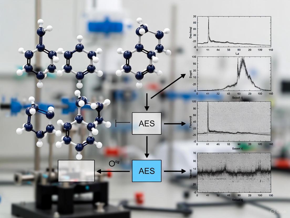
The Auger emission process involves a precise three-step sequence occurring within the atom. Figure 1 illustrates this cascade of events, which begins when an incident high-energy electron from the primary beam ejects a core-level electron (e.g., from the K-shell), creating a vacancy and leaving the atom in a highly excited, unstable state [7]. Subsequently, an electron from a higher-energy level (e.g., the L₁-shell) relaxes and fills the core-level vacancy. The energy released during this relaxation process is transferred to a third electron (e.g., from the L₂,₃-shell), which is then ejected from the atom as an Auger electron [7]. This ejected electron is the analytical signal measured in AES.
The kinetic energy of the emitted Auger electron is approximately given by Eₖ = Eₖ - Eₗ₁ - Eₗ₂,₃, where E represents the binding energy of the respective electron shells. This energy is characteristic of the specific atomic energy levels involved and is largely independent of the incident electron beam energy, making it a reliable fingerprint for elemental identification [7]. The entire process is labeled according to the electron shells involved in the transition. For example, a KLL transition involves an initial vacancy in the K-shell, an L-shell electron filling that vacancy, and the ejection of another L-shell electron.
Figure 1: The Three-Stage Auger Electron Emission Process
Spectral Data Presentation
AES spectra can be presented in two primary forms: direct (N(E) vs. E) and differentiated (dN(E)/dE vs. E) [7]. The direct spectrum plots the number of electrons (N) detected at each energy level (E), revealing the elemental composition through peak positions. However, the differentiated spectrum, which mathematically enhances small changes in the slope of the direct spectrum, is often preferred for qualitative analysis because it better resolves overlapping peaks and enhances visibility of small peaks against the background [7]. This differentiation is particularly valuable for identifying elements present in low concentrations or distinguishing between elements with closely spaced Auger transitions.
Characteristic AES Energies for Elemental Identification
Elemental Fingerprint Library
Qualitative elemental analysis in AES relies on comparing the kinetic energies of peaks in an unknown spectrum with reference data from known elements. Each element exhibits characteristic Auger transitions at specific energy ranges, creating a unique spectral fingerprint. Table 1 presents characteristic AES transition energies for selected elements, demonstrating the elemental-specific nature of these measurements [7].
Table 1: Characteristic AES Transitions and Kinetic Energies for Selected Elements
| Atomic Number | Element | AES Transition | Kinetic Energy (eV) |
|---|---|---|---|
| 3 | Li | KLL | 43 |
| 4 | Be | KLL | 104 |
| 5 | B | KLL | 179 |
| 6 | C | KLL | 272 |
| 7 | N | KLL | 379 |
| 8 | O | KLL | 508 |
| 9 | F | KLL | 647 |
| 11 | Na | KLL | 990 |
| 12 | Mg | KLL | 1186 |
| 13 | Al | LMM | 68 |
| 14 | Si | LMM | 92 |
| 15 | P | LMM | 120 |
| 16 | S | LMM | 152 |
| 17 | Cl | LMM | 181 |
| 19 | K | KLL | 252 |
| 20 | Ca | LMM | 291 |
| 21 | Sc | LMM | 340 |
| 22 | Ti | LMM | 418 |
| 23 | V | LMM | 473 |
| 24 | Cr | LMM | 529 |
| 25 | Mn | LMM | 589 |
| 26 | Fe | LMM | 703 |
The pattern of transitions follows predictable trends across the periodic table. Lighter elements (atomic number < 14) typically exhibit KLL transitions, while medium and heavier elements show LMM and MNN transitions respectively [7]. The specific kinetic energies increase with atomic number within transition series, providing a systematic framework for element identification. Modern AES instruments include comprehensive digital libraries containing characteristic spectra for most elements, enabling automated peak identification, though researcher verification remains crucial for accurate interpretation, particularly for complex samples with multiple overlapping peaks.
Chemical State Information
While AES is primarily used for elemental identification rather than detailed chemical state analysis (unlike XPS), subtle shifts in Auger peak positions and shapes can provide some chemical information [6] [7]. Changes in the oxidation state of an element can cause measurable shifts in Auger peak energies due to alterations in the binding energies of the electrons involved in the Auger process. For example, the energy required to remove an electron from Fe³⁺ is greater than from Fe⁰, resulting in a lower kinetic energy for the Fe³⁺ Auger peak compared to the metallic iron peak [7]. These chemical shifts, while typically smaller than in XPS, can still provide valuable insights into surface chemistry, oxidation states, and chemical environment when interpreted carefully by experienced analysts.
Experimental Protocols for AES Analysis
Sample Preparation Protocol
Proper sample preparation is critical for successful AES analysis. The following protocol ensures optimal results:
- Sample Cleaning: Remove surface contaminants using appropriate solvents (e.g., methanol, acetone) with lint-free wipes or through plasma cleaning. Avoid touching the analysis area with bare hands.
- Mounting: Secure samples onto appropriate holders using conductive tape or clips. Ensure electrical contact for conducting samples to prevent charging.
- Non-Conductive Samples: For insulating materials, apply a thin carbon tape path to the analysis area or use a miniature electron flood gun if available.
- Size Considerations: Ensure samples conform to instrument stage specifications, typically ≤1 cm thick for standard systems. EAG laboratories report capability to analyze wafers up to 300mm [6].
- Vacuum Compatibility: Verify samples are compatible with high vacuum conditions (typically 10⁻⁹ to 10⁻¹⁰ Torr) and will not outgas significantly.
- Reference Materials: Include well-characterized standard materials when performing quantitative analysis to verify instrument calibration.
Instrument Calibration and Data Acquisition
Figure 2 illustrates the complete workflow for AES spectral acquisition and interpretation, from sample loading through elemental identification. The following protocol ensures proper instrument setup:
- Energy Calibration: Calibrate the electron energy analyzer using standard reference materials with known Auger peaks, such as pure silver (Ag MNN peak at 356 eV) or copper (Cu LMM peak at 920 eV).
- Electron Beam Parameters: Set primary beam energy typically between 3-25 keV based on sample properties and analysis requirements [6]. Higher beam energies provide greater excitation but may increase sample damage risk.
- Beam Current Optimization: Adjust beam current (typically 0.1-100 nA) to balance signal intensity with spatial resolution and sample damage considerations.
- Spectral Acquisition: Collect survey spectra from 0-2000 eV to identify all detectable elements. Use step sizes of 0.5-1 eV for survey scans and 0.1-0.2 eV for high-resolution regional scans.
- Differentiated Spectra: Acquire spectra in differentiated mode (dN(E)/dE) for enhanced peak visibility, particularly for minor elements [7].
- Spatial Mapping: For heterogeneous samples, acquire elemental maps by rastering the electron beam across regions of interest and recording AES signal intensity at characteristic energies.
Figure 2: AES Spectral Acquisition and Interpretation Workflow
Peak Identification Methodology
The following step-by-step protocol ensures systematic identification of elements in AES spectra:
- Major Peak Identification: Identify the most intense peaks in the spectrum and match them with characteristic transitions of likely elements based on sample composition.
- Secondary Peak Verification: Confirm identifications by locating less intense Auger transitions for the same elements, following expected transition series (KLL, LMM, MNN).
- Spectral Library Comparison: Compare unknown spectra with reference spectra from standardized databases, ensuring acquisition parameters match as closely as possible.
- Peak Overlap Resolution: For overlapping peaks, use high-resolution scanning or mathematical deconvolution to separate contributions from different elements.
- Chemical State Assessment: Note peak position shifts that may indicate chemical state differences, comparing with reference data for known compounds when available.
- Quantitative Analysis: Apply sensitivity factors to determine atomic concentrations for identified elements when quantitative analysis is required.
Advanced Applications and Complementary Techniques
Research Applications
AES provides critical analytical capabilities for diverse research applications, particularly where surface composition and nanoscale features determine material performance:
- Defect and Particle Analysis: Identify sub-µm particles and surface defects to determine contamination sources and investigate failure causes in electronic devices [6]. The high spatial resolution (≥10 nm) enables analysis of features inaccessible to many other techniques.
- Thin Film Characterization: Determine composition and thickness of thin films and multilayer structures, particularly valuable for films too thin for EDS analysis [6].
- Interface Analysis: Investigate interfacial composition and reactions using depth profiling combined with ion sputtering, revealing elemental distributions as a function of depth.
- Corrosion and Oxidation Studies: Analyze surface oxide layers, including determination of oxide layer thickness on electro-polished medical devices [6].
- Grain Boundary Analysis: Identify grain boundary segregation and contamination in metal fractures, fatigues, and failures [6].
Complementary Techniques
While AES provides powerful surface analysis capabilities, it is often combined with complementary techniques for comprehensive materials characterization:
- Scanning Electron Microscopy (SEM): The electron column in AES systems typically provides high-resolution SEM imaging, enabling precise location of analysis features [6].
- Energy Dispersive X-ray Spectroscopy (EDS): Combined AES-EDS systems provide simultaneous surface (AES) and bulk (EDS) compositional information [8].
- Focused Ion Beam (FIB): Integrated FIB systems enable in situ cross-sectioning for subsurface AES analysis of buried interfaces and defects [8].
- X-ray Photoelectron Spectroscopy (XPS): While both are surface-sensitive, XPS provides more detailed chemical state information, complementing AES elemental analysis [6].
Technical Specifications and Limitations
AES Capabilities and Constraints
Table 2 summarizes the key technical specifications and limitations of AES for research applications. Understanding these parameters is essential for appropriate experimental design and interpretation of results.
Table 2: AES Technical Specifications and Analytical Capabilities
| Parameter | Specification | Notes/Implications |
|---|---|---|
| Elements Detected | Li to U | Cannot detect H or He [6] |
| Detection Limits | 0.1-1 at% (sub-monolayer) | Varies by element and matrix [6] |
| Lateral Resolution | ≥10 nm | High spatial resolution for small features [6] |
| Analysis Depth | 3-10 nm | Extreme surface sensitivity [6] |
| Depth Profiling | 2-20 nm resolution | With sputtering capability [6] |
| Quantitative Accuracy | Semi-quantitative | Requires standards for improved accuracy [6] |
| Chemical State Information | Limited | Less detailed than XPS [6] |
| Sample Requirements | Vacuum compatible | No outgassing, typically solid conductors [6] |
| Mapping Capability | Yes | Elemental distribution imaging [6] |
The Scientist's Toolkit: Essential Research Materials
Table 3: Essential Research Reagent Solutions and Materials for AES Analysis
| Item | Function/Application |
|---|---|
| Conductive Adhesive Tapes | Mounting samples to holders while maintaining electrical conductivity |
| Reference Standard Materials | Instrument calibration and quantitative analysis verification (e.g., pure Cu, Ag, Si) |
| Sputter Ion Source (Ar⁺) | Surface cleaning and depth profiling through controlled material removal |
| Electron Flood Gun | Charge compensation for analysis of insulating samples |
| Ultrasonic Cleaning Solvents | Sample surface preparation (high-purity acetone, methanol, isopropanol) |
| Specialized Sample Holders | Accommodation of various sample geometries and sizes |
| Focused Ion Beam (FIB) System | In situ cross-sectioning for subsurface analysis [8] |
| Energy Dispersive X-ray Spectrometer | Complementary bulk elemental analysis [8] |
Auger Electron Spectroscopy remains an indispensable technique for surface elemental analysis, offering unique capabilities for nanoscale characterization with high spatial resolution and surface sensitivity. The interpretation of AES spectra through characteristic kinetic energies provides reliable elemental identification when performed following systematic protocols. For researchers in drug development, materials science, and semiconductor technology, AES delivers crucial information about surface composition, contamination, and thin film structures that directly impact material performance and reliability. As AES continues to evolve with advancements in automation, spatial resolution, and integration with complementary techniques like FIB and EDS, its applications in both fundamental research and industrial problem-solving continue to expand, solidifying its position as a cornerstone of modern surface analysis.
Executing AES Analysis: From Sample to Data in the Lab
Auger Electron Spectroscopy (AES) is a powerful, surface-sensitive analytical technique that provides quantitative elemental information from the top 3-10 nm of solid materials [9] [8]. It is based on the analysis of low-energy electrons emitted during the Auger process, which follows the ionization of an atom by a high-energy electron beam. Due to the limited escape depth of these electrons, AES is exceptionally well-suited for investigating surface composition, thin films, and nanoscale features, making it indispensable in materials science, semiconductor development, and corrosion studies [10] [9]. This protocol details the complete experimental workflow within the context of advanced surface analysis research.
Fundamental Principles and Instrumentation
The AES effect occurs when a high-energy electron beam (typically 2-10 keV) ejects a core-level electron from a sample atom [10] [9]. An electron from a higher energy level then fills this vacancy, and the excess energy is released by emitting a second electron—the Auger electron. The kinetic energy of this Auger electron is characteristic of the emitting element, providing a fingerprint for elemental identification [9].
A modern AES instrument, essentially an advanced Scanning Electron Microscope (SEM), integrates several key components to perform this analysis [9]:
- Ultra-High Vacuum (UHV) System: Operates at pressures <10⁻⁹ torr. This is critical to prevent scattering of Auger electrons by gas molecules and to protect the clean sample surface from contamination [9].
- Electron Source: A field emission electron gun that produces a highly focused beam, enabling spatial resolution down to ~8-25 nm [10] [9].
- Electron Energy Analyzer: A Cylindrical Mirror Analyzer (CMA) is commonly used to measure the kinetic energy of emitted electrons with high collection efficiency and energy resolution [9].
- Ion Sputter Gun: A focused beam of argon ions (Ar⁺) used for cleaning the sample surface and for depth profiling by sequentially removing atomic layers [9].
- Secondary Detectors: Many systems are equipped with Energy Dispersive X-ray Spectroscopy (EDS) and Electron Backscatter Diffraction (EBSD) detectors for complementary bulk compositional and crystallographic analysis [9].
Table 1: Core Instrumental Components of an AES System
| Component | Function | Typical Operational Parameters |
|---|---|---|
| Electron Gun | Generates the primary excitation beam for sample ionization. | Energy: 2-10 keV; Beam Diameter: > ~25 nm [10] [9] |
| Cylindrical Mirror Analyzer (CMA) | Separates and counts emitted electrons by their kinetic energy. | Varies to achieve desired energy resolution [9]. |
| Ion Sputter Gun | Removes surface contaminants and performs depth profiling. | Ar⁺ ions; sputter rate calibrated with standards (nm/sec) [9]. |
| UHV System | Maintains a contamination-free environment for analysis. | Pressure < 10⁻⁹ torr [9]. |
Experimental Protocols: A Step-by-Step Workflow
Sample Preparation Protocol
Objective: To prepare a sample compatible with UHV and suitable for AES analysis.
- Step 1: Sample Selection and Sizing. Use small, solid samples (a few mm). Flat surfaces are preferred to minimize charging and improve spatial resolution in elemental maps [9].
- Step 2: Cleaning. If possible, clean the sample with solvents (e.g., ethanol, acetone) in an ultrasonic bath to remove organic contaminants. Dry with inert gas.
- Step 3: Mounting. Mount the sample on a suitable holder using conductive adhesives (e.g., colloidal graphite paint) or indium foil to ensure electrical and thermal contact [9].
- Step 4: Handling. Use powder-free gloves and clean tweezers to avoid introducing surface contaminants.
Sample Loading and Vacuum Stabilization Protocol
Objective: To safely introduce the sample into the UHV chamber without compromising the vacuum.
- Step 1: Transfer. Place the mounted sample into the UHV introduction chamber.
- Step 2: Pump-Down. Close the introduction chamber and begin pumping. Gradually pump down from atmospheric pressure to the UHV range (<10⁻⁹ torr). This process may take several hours.
- Step 3: Transfer to Analysis Stage. Once the UHV in the main chamber is stable, transfer the sample from the introduction chamber to the analytical stage.
In-Situ Surface Cleaning Protocol
Objective: To remove native oxide layers and adventitious carbon from the analysis area.
- Step 1: Ion Gun Setup. Align the ion sputter gun with the sample surface. Use a rastered beam over an area larger than the region of interest to ensure uniform cleaning [9].
- Step 2: Sputtering. Sputter the surface with Ar⁺ ions. Typical parameters include an accelerating voltage of 0.5-5 keV and a calibrated sputter rate. The duration depends on the contaminant thickness [9].
- Step 3: Verification. Acquire a wide-scan Auger survey spectrum (see Section 3.4) to confirm the reduction of carbon and oxygen peaks.
Data Acquisition and Analysis Protocols
Protocol 3.4.1: Auger Survey Scan Objective: To identify all elements present on the sample surface (except H and He).
- Setup: Position the electron beam on the region of interest. Set the electron beam energy to 10 keV.
- Analyzer Settings: Configure the CMA for a wide energy range scan (e.g., 0-2000 eV).
- Acquisition: Acquire the spectrum, which plots the differentiated signal (dN(E)/dE) versus electron kinetic energy. Identify elements by the positions of their characteristic Auger peaks [9].
Protocol 3.4.2: High-Resolution Multiplex Scan Objective: To determine the chemical state or obtain more precise elemental quantification.
- Setup: Based on the survey scan, select the specific energy window for a core-level transition of the element of interest (e.g., the Carbon KLL transition around 270 eV).
- Acquisition: Acquire a high-resolution, non-differentiated spectrum over this narrow energy window.
- Analysis: Use peak fitting routines to deconvolute chemical shifts, which can indicate different bonding states [9].
Protocol 3.4.3: AES Elemental Mapping Objective: To visualize the lateral distribution of elements on the surface.
- Setup: Define the analysis area on the SEM image.
- Tuning: Set the CMA to the kinetic energy of the primary Auger peak for the element of interest.
- Rastering: Raster the focused electron beam across the selected area.
- Data Collection: At each pixel, record the intensity of the Auger peak. Construct a 2D map where brightness corresponds to elemental concentration [10] [8].
Protocol 3.4.4: Depth Profiling Objective: To determine the elemental composition as a function of depth.
- Setup: Select a sample area for analysis.
- Cycling: Alternate between two processes:
- Sputter Cycle: Remove a thin layer of material using the Ar⁺ ion gun for a predetermined time.
- Analysis Cycle: Acquire Auger survey spectra or multiplex scans from the newly exposed surface [9].
- Repetition: Repeat this cycle until the desired depth is reached.
- Data Processing: Plot elemental concentrations (from peak-to-peak heights in differentiated spectra) versus sputter time or calibrated depth.
Data Presentation and Quantitative Analysis
AES data is semi-quantitative, and concentrations can be calculated using relative sensitivity factors. The atomic concentration of an element A is given by:
C_A = (I_A / S_A) / Σ(I_n / S_n)
Where I_A is the measured Auger peak intensity for element A, S_A is its relative sensitivity factor, and the sum is over all detected elements n.
Table 2: Key Analytical Capabilities and Performance Metrics of AES
| Analytical Feature | Performance Metric | Notes & Limitations |
|---|---|---|
| Detection Limit | ~0.1 at% (for elements Z≥3/Li and heavier) [9]. | Varies by element and matrix. |
| Surface Sensitivity | ~3-10 nm (0.4-10 atomic monolayers) [9] [8]. | Due to the short escape depth of Auger electrons. |
| Lateral Resolution | < 25 nm with field emission source [10] [9]. | Allows for sub-micron mapping of small features. |
| Elements Detected | All except H and He [9]. | Light element analysis is a particular strength. |
| Quantitative Analysis | Semi-quantitative using sensitivity factors [9]. | Can be more accurate with standard samples. |
| Sample Requirements | Solid, UHV-compatible, vacuum-stable. | Volatile or beam-sensitive samples (epoxies, organics) are unsuitable [9]. |
Visualizing the AES Workflow and Process
The Auger Emission Process
The following diagram illustrates the fundamental physical process that generates an Auger electron.
AES Experimental Workflow
This flowchart outlines the end-to-end operational procedure for a standard AES analysis, from sample preparation to data interpretation.
The Scientist's Toolkit: Essential Research Reagents and Materials
Table 3: Essential Materials and Reagents for AES Experiments
| Item | Function / Application |
|---|---|
| Conductive Adhesives (e.g., Colloidal Graphite Paint, Silver Paste) | Ensures electrical and thermal contact between the sample and holder, mitigating charging effects on insulating samples [9]. |
| Indium Foil/Substrate | A malleable, conductive mounting medium, especially useful for pressing and securing small or powdered samples [9]. |
| Argon (Ar) Gas | The source gas for the ion sputter gun, used for in-situ surface cleaning and depth profiling [9]. |
| Silicon Wafer Substrates | A clean, flat, and conductive substrate often used for mounting powdered or irregular samples [9]. |
| Standard Reference Materials (e.g., oxide-coated metal standards) | Used for calibrating the sputter rate of the ion gun, converting sputter time to accurate depth measurements [9]. |
| Solvents (e.g., High-Purity Isopropanol, Acetone) | For preliminary cleaning of samples to remove gross organic contamination prior to insertion into the UHV chamber. |
Auger Electron Spectroscopy (AES) is a powerful surface-sensitive analytical technique used for elemental identification and compositional analysis of solid surfaces. Within the broader context of AES surface analysis experimental procedure research, mastering qualitative and semi-quantitative analysis is fundamental. AES excels at providing high-lateral-resolution compositional information, capable of identifying all elements except hydrogen and helium with a sensitivity down to approximately 0.5 atomic percent (at.%) [10] [11]. The core principle of AES involves bombarding a sample surface with a focused beam of high-energy (2-10 kV) electrons. This incident beam causes the emission of "Auger electrons," which possess discrete kinetic energies characteristic of the elements from which they originated [10]. By analyzing the kinetic energies of these electrons, a qualitative identification of the surface elements is achieved. Quantitative and semi-quantitative analysis then builds upon this by interpreting the intensities of the measured Auger signals [11].
A key challenge in AES, particularly when analyzing insulating materials, is the accumulation of surface charge, which can distort results. The severity of this effect is governed by the Total Secondary Electron Yield (TSEY), defined as the ratio of the number of outgoing electrons to the number of incident electrons (σ = Iₒ/Iᵢ) [11]. A stable analysis condition is theoretically achieved when σ = 1, meaning the incident and outgoing electron currents are balanced, thus preventing charge build-up. The ability to control this parameter is critical for obtaining reliable data from non-conductive samples, such as ceramics or polymers, which are increasingly important in various industrial and research fields [11].
Key Analytical Parameters for Quality Assessment
The quality of information obtained from AES, whether qualitative or semi-quantitative, depends on a set of key analytical parameters. Ensuring the reliability of determination results requires the identification and management of factors that could cause measurement deviations [12] [11]. Among these, selectivity and the limits of detection are paramount.
Selectivity refers to the method's ability to accurately identify and quantify a specific element in the presence of other substances within the sample matrix [12] [11]. In AES, while the characteristic Auger peaks allow for identification, overlapping peaks from different elements or matrix effects can complicate this process. Unlike techniques prone to isobaric or polyatomic interferences, AES spectra can be affected by peak shape changes and background contributions, which must be accounted for to ensure accurate qualitative analysis.
The Limit of Detection (LOD) is the lowest concentration of an element that can be reliably detected by the technique. For AES, the detection limits are typically in the range of tenths of a weight percent [12]. This makes AES exceptionally powerful for surface analysis but less suited for detecting trace elements at very low concentrations compared to other elemental analysis techniques.
Table 1: Key Parameters Affecting AES Analysis Quality
| Parameter | Impact on Qualitative/Semi-Quantitative Analysis |
|---|---|
| Selectivity | Determines the accuracy of element identification in a complex matrix; affected by peak overlap and chemical state shifts [12]. |
| Limit of Detection (LOD) | ~0.5 at.% sensitivity; defines the lowest elemental concentration that can be detected [12] [10]. |
| Spatial Resolution | The size of the smallest feature that can be analyzed; can be as high as ~70 nm for insulating samples and even better for conductors [10] [11]. |
| Surface Charging | Can cause energy shifts, peak broadening, and deformation, severely impacting both identification and quantification, especially on insulators [11]. |
Experimental Protocols for Analysis
Obtaining high-quality AES data requires careful experimental procedures. The following protocols outline the critical steps for both qualitative and semi-quantitative analysis, with specific considerations for challenging insulating samples.
Protocol for Qualitative Elemental Identification and Mapping
This protocol is designed for the initial identification of elements present on a sample surface and for visualizing their spatial distribution.
- Sample Preparation (Insulating Samples):
- Charge Compensation Method (Bulk Samples): Metallize the sample surface with a thin, conductive coating (e.g., Au, C). This facilitates surface charge dissipation [11].
- Thin Film Method: Thin the insulating sample to less than 100 nm. Analyze it with a high-energy primary electron beam to penetrate the sample and reduce charge accumulation [11].
- Instrument Setup:
- Mount the sample securely on the holder, ensuring good electrical contact if possible.
- For bulk insulating samples, implement charge compensation by flooding the analysis area with low-energy Ar⁺ ions to neutralize surface charge [11].
- Optimize the primary electron beam parameters. To minimize charging, use a reduced beam current and adjust the beam energy and incident angle to favor a TSEY (σ) value near or above 1 [11].
- Survey Analysis:
- Acquire a wide-energy-range Auger survey spectrum (e.g., 0-1000 eV or higher) from a representative area.
- Identify all elements present by matching the kinetic energies of the major peaks in the spectrum to standard reference databases.
- High-Resolution Mapping:
- Define the elements of interest based on the survey spectrum.
- Select a specific Auger transition peak for each element and set the electron energy analyzer to measure the intensity at that energy.
- Raster the focused electron beam across the region of interest to generate an elemental map, demonstrating the lateral distribution of each element with high resolution (e.g., 70 nm) [11].
Protocol for Semi-Quantitative Analysis
This protocol describes a method for estimating the relative atomic concentrations of elements identified on the surface.
- Peak Acquisition:
- Following qualitative identification, acquire high-resolution, multiplex spectra for the specific Auger peaks of each identified element.
- Ensure the spectral acquisition parameters are consistent across all measurement points.
- Data Processing:
- Measure the peak-to-peak height (or integrated peak area) in the derivative spectrum for each elemental peak.
- This measured intensity (I) for an element 'X' is proportional to its concentration.
- Concentration Calculation:
- Calculate the atomic concentration (Cₓ) of each element using a relative sensitivity factor (RSF) approach. The formula for the semi-quantitative estimate is:
Cₓ = [ (Iₓ / Sₓ) / Σ (Iᵢ / Sᵢ) ] * 100%where:Iₓis the measured peak intensity of element X.Sₓis the relative sensitivity factor for element X.Σ (Iᵢ / Sᵢ)is the sum of the intensity/RSF ratios for all elements detected.
- Use RSFs derived from standard reference materials measured under identical analytical conditions for the most accurate results [11].
- Calculate the atomic concentration (Cₓ) of each element using a relative sensitivity factor (RSF) approach. The formula for the semi-quantitative estimate is:
The Scientist's Toolkit: Essential Research Reagents and Materials
Successful AES analysis requires specific materials and standards to ensure accurate and reproducible results.
Table 2: Key Research Reagent Solutions and Materials for AES
| Item | Function/Application |
|---|---|
| Conductive Coatings (Gold, Carbon) | Sputter-coated onto insulating samples to provide a path for charge dissipation during the Charge Compensation Method [11]. |
| Standard Reference Materials (e.g., Si₃N₄, Al₂O₃ bulk) | Well-characterized materials used to determine element-specific Relative Sensitivity Factors (RSFs) for accurate semi-quantification [11]. |
| Low-Energy Ar⁺ Ion Gun | Provides a flux of positive ions to neutralize negative charge build-up on the surface of insulating samples during analysis [11]. |
| Focus Ion Beam (FIB) / Ultramicrotome | Equipment used for the precise preparation of ultrathin sample sections (<100 nm) required for the Thin Film Method of analyzing insulators [11]. |
| High-Purity Polishing Materials | Used to prepare a flat, smooth, and uncontaminated surface on solid samples, which is critical for reproducible and quantitative analysis. |
Workflow and Data Analysis Visualization
The following diagram illustrates the logical workflow for conducting a complete AES analysis, from sample preparation through to qualitative and semi-quantitative results.
Comparative Analysis with Other Elemental Techniques
AES is one of several powerful tools for elemental bioimaging and analysis. Its capabilities and limitations become clear when compared to other common techniques. The choice of technique depends on the specific requirements of the analysis, such as the needed spatial resolution, detection limits, and whether the sample is conductive or insulating.
Table 3: Comparison of Elemental Analysis and Imaging Techniques
| Feature | AES | XRF | SEM-EDS | LA-ICP-MS |
|---|---|---|---|---|
| Full Name | Auger Electron Spectroscopy | X-ray Fluorescence | Scanning Electron Microscopy with Energy-Dispersive X-ray | Laser Ablation Inductively Coupled Plasma Mass Spectrometry |
| Spatial Resolution | ~70 nm (for insulators) to ~25 nm [10] [11] | ~0.05-100 µm [12] | ~1 µm [12] | 5-100 µm [12] |
| Detection Limit (LOD) | ~0.5 at.% [10] | mg/kg [12] | Tenths of weight % [12] | µg/kg [12] |
| Quantification | Semi-Quantitative [11] | Yes [12] | Semi-Quantitative [12] | Yes (Fully Quantitative) [12] |
| Sample Destruction | Semi-non-destructive | No | No | Semi-non-destructive [12] |
| Key Advantage | Excellent lateral resolution for surface elemental analysis; depth profiling. | Good for bulk analysis; minimal sample prep. | Widely available; combined with high-resolution imaging. | Excellent sensitivity (low LODs); fully quantitative. |
Auger Electron Spectroscopy (AES) is a powerful surface-sensitive analytical technique that provides exceptional insights into the elemental composition and chemical environment of material surfaces. Based on the Auger effect, discovered independently by Lise Meitner and Pierre Auger in the 1920s, AES has evolved into an indispensable tool for characterizing the outermost atomic layers (typically 2-5 nm) of solid surfaces [1]. The fundamental Auger process occurs when an electron beam (typically 3-20 keV) strikes a sample, ejecting a core-level electron. This creates an unstable ion that relaxes through a radiationless process where an electron from a higher energy level fills the core hole, simultaneously transferring energy to a third electron (the Auger electron) that is emitted from the atom [1].
The kinetic energy of the emitted Auger electron is characteristic of the specific atomic transition and is approximately given by the relationship: EABC = EA - EB - EC, where EA, EB, and EC represent the binding energies of the atomic levels involved in the transition [1]. This fundamental relationship makes AES highly sensitive to chemical state variations, as changes in the chemical environment alter the effective binding energies of the participating electrons, resulting in measurable shifts in Auger peak positions and changes in lineshapes. Chemical state analysis through AES enables researchers to identify oxidation states, characterize chemical bonding environments, detect surface contaminants, and investigate interfacial reactions in diverse materials systems ranging from catalysts to semiconductors [13] [14].
Theoretical Foundation of AES Chemical Shifts
The Auger Process and Energy Considerations
The Auger effect involves a three-electron process that produces characteristic electrons whose energies are independent of the incident beam energy, making AES particularly valuable for chemical analysis. When an atom is excited by an external mechanism (electron beam, photons, or ions), a core-level electron is removed, creating a hole in an inner orbital. During the subsequent relaxation process, an electron from a higher energy level fills this vacancy, and the transition energy is transferred to a third electron that is emitted from the atom [1]. The kinetic energy of this emitted Auger electron can be calculated using the formula:
Ekin = ECore State - EB - EC'
Where ECore State is the energy of the core level where the initial vacancy was created, EB is the binding energy of the electron that fills the core hole, and EC' is the binding energy of the emitted electron in the presence of the core hole [1]. The presence of the core hole significantly influences the energy levels, making Auger transitions particularly sensitive to the chemical environment.
Chemical Influences on Auger Spectra
Chemical state information in AES is derived primarily from two spectral features: peak energy shifts and lineshape modifications. When an atom undergoes a change in its chemical environment (such as oxidation, formation of compounds, or coordination changes), the electron density distribution around the atom is altered. This affects the binding energies of the electrons involved in Auger transitions, leading to measurable shifts in peak positions [14]. The lineshape changes occur because the valence band density of states, which often participates in Auger transitions, is directly modified by chemical bonding.
For example, when analyzing semiconductor surfaces like GaP and Si, researchers have observed significant differences in the Auger signals between atomically clean surfaces and those exposed to the atmosphere. The clean surfaces exhibit characteristic Auger transitions, while oxidized surfaces show modified peak positions and intensities due to the formation of oxide species [14]. These chemical effects are particularly pronounced in Auger transitions involving valence electrons (such as LVV transitions), making them more sensitive to chemical state variations than core-core-core transitions.
Table 1: Types of Chemical Information Obtainable from AES Spectra
| Spectral Feature | Chemical Information | Example Transitions |
|---|---|---|
| Peak Position Shift | Oxidation state, electronegativity effects | Si LVV, P LVV, O KLL |
| Lineshape Modification | Chemical bonding, valence band structure | CVV transitions in metals and semiconductors |
| Peak Intensity Changes | Compound formation, overlayer growth | Elemental ratios during thin film growth |
| Peak Width Changes | Lifetime effects, multiple environments | Transition metals in different coordination spheres |
Quantitative Data and Reference Values
The interpretation of chemical state information in AES requires reference to established data from well-characterized standards. The following tables summarize key quantitative information essential for chemical state analysis.
Table 2: Characteristic AES Peak Shifts for Common Elements
| Element | Chemical State | Transition | Peak Energy (eV) | Shift (eV) | Application Context |
|---|---|---|---|---|---|
| Silicon (Si) | Elemental Si | LVV | 92 | Reference | Clean semiconductor surfaces [14] |
| SiO₂ | LVV | 78 | -14 | Oxide layer characterization [14] | |
| Phosphorus (P) | Elemental P | LVV | 120 | Reference | GaP surfaces [14] |
| P₂O₅ | LVV | ~115 | ~-5 | Surface oxidation [14] | |
| Carbon (C) | Graphite | KLL | 272 | Reference | Reference carbon |
| Carbide | KLL | ~262 | ~-10 | Metal carbide identification | |
| Hydrocarbon | KLL | ~268 | ~-4 | Contamination layers | |
| Oxygen (O) | Metal oxides | KLL | 503-510 | Variable | Oxide characterization [14] |
Table 3: Experimental Parameters Affecting AES Spectral Resolution
| Parameter | Effect on Chemical Shift Resolution | Optimal Values for Chemical State Analysis |
|---|---|---|
| Primary Beam Energy | Ionization cross-section, damage potential | 3-10 keV (balance between signal and damage) [14] |
| Beam Current | Signal-to-noise ratio, spatial resolution | 10-100 nA (higher for better SNR) |
| Modulation Voltage | Peak resolution, derivative spectrum quality | 2-5 V (lower for better peak separation) [1] |
| Scan Rate | Peak position accuracy, signal quality | Slow scans (0.1-0.5 eV/s) for high resolution [15] |
| Time Constant | Signal filtering, distortion minimization | 0.1-0.3 s (matched to scan rate) [15] |
Experimental Protocols for Chemical State Analysis
Sample Preparation Protocol
Objective: To prepare contamination-free surfaces suitable for reproducible AES chemical state analysis.
Materials Required:
- UHV-compatible sample holder
- Metal tweezers (stainless steel or tantalum)
- Solvent cleaning supplies (isopropanol, acetone)
- Glove box or transfer system for air-sensitive samples
Procedure:
- Initial Cleaning: Begin by ultrasonically cleaning samples in sequential solvent baths (acetone followed by isopropanol) for 5 minutes each to remove gross organic contamination.
- UHV Transfer: Mount the sample on a UHV-compatible holder using minimal-contact techniques to prevent surface damage.
- In-situ Cleaning: Inside the UHV system, employ one or more of the following cleaning methods based on sample compatibility:
- Ar⁺ Ion Sputtering: Use 0.5-4 keV Ar⁺ ions at current densities of 1-10 μA/cm² for 1-30 minutes, depending on contamination thickness. Follow with mild annealing if necessary to restore surface order.
- Annealing: Resistively heat the sample to temperatures appropriate for the material (typically 400-800°C for metals, lower for semiconductors) to desorb surface contaminants.
- In-situ Cleaving: For brittle materials like semiconductors, use a precision cleaving system to create fresh, atomically clean surfaces [14].
- Cleanliness Verification: Acquire a survey AES spectrum (0-1000 eV) to confirm the absence of carbon, oxygen, and other contaminants before proceeding with chemical state analysis.
AES Data Acquisition for Chemical Shift Analysis
Objective: To acquire high-quality AES spectra suitable for chemical state identification with minimal beam-induced damage.
Materials Required:
- AES spectrometer with cylindrical mirror analyzer (CMA) or hemispherical analyzer
- Electron gun with adjustable energy and current
- Sample holder with precise positioning capabilities
Procedure:
- Instrument Calibration:
- Energy calibrate the analyzer using standard reference materials (Au, Ag, or Cu).
- Verify energy resolution using a known sharp peak (e.g., Cu MVV at 61 eV) with full width at half maximum (FWHM) typically <0.5 eV.
- Preliminary Survey Scan:
- Acquire a broad survey spectrum (0-1000 eV) using: Primary energy: 10 keV, Beam current: 100 nA, Modulation voltage: 5 Vₚₚ, Scan rate: 5 eV/s.
- Identify all elements present and their approximate concentrations.
- High-Resolution Regional Scans:
- For each element of interest, acquire high-resolution regional scans around the relevant Auger transitions:
- Set primary energy to 3-5 keV to minimize damage while maintaining sufficient signal.
- Reduce beam current to 10-20 nA for beam-sensitive materials.
- Use lower modulation voltage (1-2 Vₚₚ) for direct spectrum acquisition.
- Implement slow scan rates (0.1-0.5 eV/s) with multiple scans averaged for improved signal-to-noise.
- For each element of interest, acquire high-resolution regional scans around the relevant Auger transitions:
- Derivative Spectrum Acquisition (optional):
- For enhanced peak visibility, acquire derivative spectra by applying a small AC modulation (1-2 Vₚₚ) to the analyzer and using lock-in amplification.
- Note that derivative spectra can complicate quantitative lineshape analysis but are excellent for peak identification.
- Damage Minimization:
- Continuously monitor peak shapes and positions during acquisition to detect beam-induced damage.
- For sensitive materials, use rastered beam acquisition or frequently move to fresh sample areas.
Chemical Shift Measurement and Interpretation Protocol
Objective: To accurately measure and interpret chemical shifts in AES spectra for chemical state identification.
Materials Required:
- Reference materials with known chemical states
- Spectral analysis software with peak fitting capabilities
- Database of standard AES spectra
Procedure:
- Energy Referencing:
- Reference all spectra to a well-established internal standard (e.g., adventitious carbon C KLL at 272 eV) or external standard.
- Apply consistent energy calibration across all samples in a study.
- Background Subtraction:
- Apply appropriate background subtraction (typically Shirley or Tougaard background) to remove inelastic scattering contributions.
- Use consistent parameters for all comparable samples.
- Peak Position Determination:
- For direct spectra: Identify peak positions as the maximum intensity point after background subtraction.
- For derivative spectra: Identify peak positions as the most negative excursion points.
- Use peak fitting with appropriate functions (Gaussian, Lorentzian, or mixed) for overlapping features.
- Chemical Shift Calculation:
- Calculate chemical shifts relative to the elemental reference state: ΔE = Esample - Eelemental
- Compare measured shifts with database values (see Table 2) for chemical state identification.
- Lineshape Analysis:
- Analyze the complete lineshape of Auger transitions, particularly for CVV transitions that reflect the local density of states.
- Compare with theoretical calculations or reference spectra for definitive chemical state assignment.
- Multivariate Analysis (for complex systems):
- Employ factor analysis or principal component analysis for samples with multiple chemical states.
- Use linear least-squares fitting with reference spectra for quantitative chemical state determination.
The Scientist's Toolkit: Essential Research Reagents and Materials
Table 4: Essential Materials for AES Chemical State Analysis
| Material/Reagent | Function in AES Analysis | Application Notes |
|---|---|---|
| Reference Standards | Energy calibration, spectral comparison | Au, Ag, Cu for energy calibration; pure elements and well-characterized compounds for chemical shift references |
| Ar⁺ Ion Sputter Source | Surface cleaning, depth profiling | Essential for removing native oxides and contamination; use low energies (0.5-2 keV) for minimal damage |
| UHV-Compatible Sample Holders | Sample mounting and positioning | Materials: Ta, Mo, or stainless steel; must maintain electrical contact for conducting samples |
| In-situ Cleaving System | Creating atomically clean surfaces | Critical for standard preparation; especially important for semiconductor and ceramic materials [14] |
| Electron Gun | Primary excitation source | Field emission guns provide superior spatial resolution; LaB₆ guns offer higher current for better SNR |
| Hemispherical Analyzer | High-energy resolution analysis | Preferred for chemical state analysis due to superior energy resolution compared to CMA |
| Charge Neutralization System | Analysis of insulating samples | Low-energy electron flood gun or Ar⁺ beam for charge compensation on insulators |
Applications in Materials Research
Catalyst Surface Analysis
AES has proven particularly valuable in catalysis research, where surface composition directly influences activity and selectivity. When studying catalyst materials such as supported metal nanoparticles, bimetallic systems, and metal oxides, AES enables researchers to correlate catalytic performance with surface chemical states [13]. For example, the oxidation state of metal nanoparticles (e.g., Pt⁰ vs. Pt²⁺) significantly impacts catalytic activity in oxidation reactions, and these states can be distinguished through careful analysis of AES peak positions and lineshapes. AES also facilitates the investigation of promoter elements and their chemical states, providing insights into their mode of action in complex catalyst formulations.
In catalyst deactivation studies, AES can identify carbonaceous deposits (coking) and distinguish between different types of carbon species (graphitic vs. amorphous carbon) through analysis of the C KLL lineshape. Similarly, poison accumulation (e.g., S, Cl) can be detected and quantified, guiding regeneration protocol development. The extreme surface sensitivity of AES makes it ideal for investigating the initial stages of catalyst preparation, such as the decomposition of precursor compounds on support materials, enabling rational catalyst design through understanding of fundamental surface processes [13].
Semiconductor Surface Characterization
Semiconductor surfaces and interfaces represent another major application area for AES chemical state analysis. As demonstrated in studies of GaP and Si surfaces, AES can effectively characterize native oxides, contamination layers, and intentional surface modifications [14]. When semiconductor surfaces are exposed to the atmosphere, they rapidly develop contamination layers containing carbonaceous species and oxides, which can be quantitatively analyzed using AES. The chemical state information is crucial for understanding electronic properties, as different oxidation states (e.g., SiO vs. SiO₂ on silicon) significantly impact interface states and device performance.
AES studies have revealed that electron irradiation during analysis can itself induce chemical changes on certain semiconductor surfaces. For instance, GaP surfaces show much greater susceptibility to electron beam effects compared to Si, with significant carbon and oxygen species deposition observed after just 3 hours of irradiation [14]. This highlights the importance of controlling acquisition parameters during AES analysis of beam-sensitive materials. For semiconductor device fabrication, AES chemical state analysis provides critical information about cleaning efficiency, interface reactions, and thin film properties, enabling process optimization and yield improvement.
Workflow Visualization
Diagram 1: AES Chemical State Analysis Workflow. This diagram outlines the complete experimental procedure for chemical state analysis using AES, highlighting critical acquisition parameters that influence spectral quality and chemical shift resolution.
Chemical state analysis through Auger Electron Spectroscopy provides a powerful approach for investigating the surface chemistry of materials with exceptional sensitivity to the local chemical environment. By carefully analyzing peak shifts and lineshape modifications in AES spectra, researchers can extract detailed information about oxidation states, chemical bonding, and surface reactions that directly influence material properties and performance. The protocols and reference data presented in this application note establish a framework for reproducible, high-quality AES chemical state analysis across diverse materials systems. When implemented with appropriate controls and validation, AES chemical shift analysis serves as an indispensable tool in surface science, enabling advances in catalyst design, semiconductor technology, and functional materials development.
Overcoming Common AES Challenges and Optimizing Data Quality
Auger Electron Spectroscopy (AES) is a powerful surface-sensitive analytical technique that provides information about the chemical composition of the outermost layers of a material, typically the top 2-3 nm [4] [5]. The principal advantages of AES include excellent spatial resolution (< 1 µm), high surface sensitivity (~20 Å), and superior detection of light elements, with detection limits for most elements ranging from about 0.01 to 0.1% (atomic) [4]. However, the technique faces significant limitations when analyzing insulating materials due to sample charging effects that can compromise data quality and integrity.
The fundamental operating principle of AES involves using a primary electron beam to excite the sample surface. When an inner-shell electron is ejected from a sample atom through interaction with a primary electron, an electron from an outer shell fills the vacancy. The energy released from this transition leads to the emission of an Auger electron, whose energy is characteristic of the element from which it was emitted [4] [16]. AES requires an ultrahigh vacuum environment to minimize the interception of Auger electrons by gas molecules between the sample and detector [4].
Table 1: Fundamental Characteristics and Limitations of AES Analysis
| Parameter | Typical Specification | Impact on Insulating Samples |
|---|---|---|
| Analysis Depth | ~2-3 nm [4] | Unaffected by sample conductivity |
| Spatial Resolution | < 1 µm [4] | Degraded by charging effects |
| Detection Limits | 0.01-0.1% (atomic) [4] | Compromised by unstable surface potential |
| Sample Environment | Ultrahigh vacuum (<1×10⁻⁹ Torr) [4] | Applicable to all sample types |
| Primary Probe | Electron beam (typically 2-25 keV) [17] | Primary source of charging |
The Sample Charging Phenomenon in Insulating Materials
The charging of insulators under electron beam irradiation presents a fundamental challenge for AES analysis. This phenomenon occurs due to the imbalance between incident electron beam current and emitted secondary electron emission current. When the total secondary electron emission yield (TSEEY, denoted as σ) is unity, an exact charge balance occurs. However, if σ is greater than unity, the surface charges positively, while σ less than unity leads to negative charging [17].
Charging manifests as both a near-instantaneous effect governed by secondary electron emission and a time-dependent effect governed by implanted charge and dynamically changing secondary electron emission. For insulating materials, the incident electron beam implants negative charge in a layer approximately 1 μm deep, while surface secondary emission may lead to either positive or negative surface charge depending on the experimental conditions [17].
The materials exhibiting the most significant charging effects, in order of increasing severity, are typically: MgO, Al₂O₃, Si₃N₄, NaCl, and SiO₂. However, this order depends significantly on the precise form and purity of the specific materials being analyzed [17]. Excessive charging can completely deflect the primary electron beam, preventing analysis entirely, or cause significant peak shifts and distortions that render quantitative analysis impossible.
Diagram 1: Charge formation mechanism and impacts on AES data.
Charge Control Strategies and Methodologies
Primary Charge Mitigation Techniques
Several practical strategies have been developed to mitigate charging effects during AES analysis of insulating materials. These approaches can be implemented individually or in combination, depending on the severity of charging and the specific instrument configuration available.
Table 2: Primary Charge Control Strategies for AES Analysis of Insulators
| Strategy | Mechanism of Action | Implementation Parameters | Effectiveness |
|---|---|---|---|
| Electron Beam Defocusing | Reduces current density, minimizing localized charge buildup | Increase beam diameter by 2-10x; raster over larger area [17] | High for moderate charging |
| Beam Energy Reduction | Shifts operation to E | Reduce beam energy to <1.5 keV; optimize using EC⁰·⁶ cos θ = constant [17] | Material-dependent |
| Sample Tilting | Increases effective σ, promoting positive surface charge | Increase angle of incidence to 30-60° from normal [17] | High for materials with high σm |
| Reduced Exposure Time | Limits total charge implantation | Work quickly; use pulsed beam techniques [17] | Essential for all analyses |
| Conductive Coating | Provides path for charge dissipation | Apply 2-10 nm carbon or metal films [16] | Very high, but alters surface |
The most effective strategy often involves a combination of these approaches. The relationship between beam energy (EC) and angle of incidence (θ) follows approximately EC⁰·⁶ cos θ = constant for low-dose studies. The constant value ranges from above 4.0 for MgO to 1.85 for SiO₂, defining a zone of low charging in EC,θ space [17]. For high-dose studies, this zone of low charging contracts, with the constant value reducing to below 0.88 of the low-dose value for SiO₂ and below 0.55 for Si₃N₄ [17].
Advanced Charge Control Methodologies
For materials exhibiting severe charging, more advanced methodologies may be required. These include the use of low-energy flood guns (electrons of ~400 eV) to stabilize surface potential, flooding the surface with low-energy He⁺ or Ar⁺ ions, exposure to UV radiation, or controlled heating of the sample [17]. Gaseous environments at specific pressures (e.g., 1×10⁻⁴ Torr Ar) can also effectively discharge samples, though this may lead to contamination for certain materials [17].
Diagram 2: Decision workflow for charge mitigation strategies.
Experimental Protocols for Insulating Samples
Pre-analysis Assessment Protocol
Material Characterization: Determine sample composition, purity, and physical form through prior characterization techniques. Document any known electrical properties or previous analysis history.
Conductivity Screening: Perform preliminary conductivity assessment using a multimeter or by observing secondary electron imaging behavior in the AES instrument.
Morphology Evaluation: Examine surface topography using secondary electron imaging at low beam currents (≤1 nA) and energies (3-5 keV) to identify optimal analysis regions.
Charge Propensity Prediction: Calculate expected charging behavior using the relationship EC⁰·⁶ cos θ = K, where K is material-specific (K ≈ 4.0 for MgO, 1.85 for SiO₂) [17].
Optimized AES Acquisition Protocol for Insulators
Initial Conditions: Begin analysis with reduced beam energy (2-3 keV), defocused beam (≥1 µm diameter), and sample tilted to 45-60° from normal incidence.
Progressive Optimization:
- Acquire initial survey scan and assess peak shape and stability
- If charging observed, further reduce beam energy in 0.5 keV increments
- Increase tilt angle incrementally up to 60° maximum
- Defocus beam to spread charge over larger area
- Reduce beam current to minimum acceptable for adequate signal-to-noise
Time-management: Limit exposure of single area to essential acquisition time only. For multiplex scans or depth profiling, monitor for time-dependent charging effects.
Validation: Compare acquired spectra with standard reference materials when possible. Verify that peak positions remain stable during acquisition.
Table 3: Troubleshooting Guide for Charging Artifacts in AES Analysis
| Observed Symptom | Probable Cause | Corrective Action | Validation Method |
|---|---|---|---|
| Progressive peak shifts to lower kinetic energy | Negative surface charge buildup | Reduce beam energy; increase tilt angle; use charge compensation | Monitor peak position stability over time |
| Peak broadening and instability | Severe, fluctuating surface potential | Defocus beam significantly; reduce beam current; use conductive coating | Check peak FWHM consistency |
| Complete signal loss or extreme distortion | Excessive charging deflecting primary beam | Apply conductive coating; use lowest possible beam energy | Verify secondary electron image quality |
| Regional variations in charging effects | Inhomogeneous sample composition | Optimize conditions for most insulating region; consider multiple area analysis | Map identical regions under different conditions |
The Scientist's Toolkit: Essential Research Reagents and Materials
Table 4: Essential Materials for AES Analysis of Challenging Samples
| Material/Reagent | Function | Application Protocol | Compatibility Notes |
|---|---|---|---|
| High-purity Carbon Rods | Thermal evaporation source for conductive coatings | Evaporate 2-5 nm films under high vacuum | Compatible with most materials; minimal spectral interference |
| Gold-Palladium Target | Sputter coating for enhanced conductivity | Sputter coat 3-8 nm films using Ar⁺ plasma | Higher conductivity than carbon; may interfere spectrally |
| Conductive Copper Tape | Sample mounting and grounding | Secure sample edges to metallic stub | Essential for proper grounding; use minimal adhesive |
| Reference Insulators (MgO, SiO₂) | Method development and calibration | Use for optimizing instrument parameters | Well-characterized charging behavior [17] |
| Argon Gas (High Purity) | Charge compensation and sputtering | Low-energy ion flooding for charge neutralization | May cause surface damage at higher energies |
| Calibration Standards (Au, Cu, Ag) | Energy scale verification | Analyze to confirm absence of charging artifacts | Essential for validating charge mitigation success |
Successful AES analysis of insulating materials requires a systematic approach to charge management that combines appropriate sample preparation, optimized instrument parameters, and strategic analysis protocols. The fundamental understanding of charging mechanisms enables analysts to select the most effective combination of strategies, whether through beam parameter optimization, sample geometry manipulation, or the application of conductive coatings. By implementing the protocols and methodologies outlined in this application note, researchers can extend the powerful capabilities of AES to a wider range of materials, including those with significant insulating properties, while maintaining data integrity and analytical reliability.
The efficacy of surface analysis techniques is fundamentally governed by the intricate balance between three critical instrumental parameters: spatial resolution, signal-to-noise ratio (SNR), and acquisition time. Achieving optimal analytical performance requires careful calibration of these interdependent factors, as enhancements in one typically come at the expense of others. For instance, pursuing higher spatial resolution often necessitates smaller analytical areas or probe sizes, which inherently reduces signal intensity and consequently demands longer acquisition times to maintain acceptable SNR levels. Similarly, attempts to shorten acquisition times can severely compromise both resolution and signal quality, potentially rendering collected data unreliable for meaningful interpretation.
Within the context of Auger Electron Spectroscopy (AES) and related surface analysis techniques, this parameter optimization challenge becomes particularly pronounced. AES provides exceptional surface sensitivity, typically analyzing the top 2-5 nanometers of a material, making it indispensable for understanding surface composition, contamination, and thin film properties. However, without systematic optimization protocols, researchers risk collecting suboptimal data that may lead to incorrect conclusions about material structure-property relationships. This document provides detailed application notes and protocols for researchers, scientists, and drug development professionals seeking to establish robust experimental procedures for AES surface analysis within their research programs.
Theoretical Framework: The Interdependence of Key Parameters
The relationship between spatial resolution, SNR, and acquisition time can be quantitatively described through fundamental physical principles. The spatial resolution in techniques like AES is primarily determined by the incident beam diameter and the interaction volume of the primary electrons with the sample. As resolution increases (smaller probe size), the analyzed volume decreases proportionally, leading to a reduction in the total signal intensity. This relationship follows a cubic dependence, as the signal generation volume decreases with the cube of the probe size reduction.
The signal-to-noise ratio in AES is governed by Poisson statistics, where the noise is proportional to the square root of the total signal. This relationship can be expressed as SNR = √(I×t), where I is the signal intensity and t is the acquisition time. Consequently, to maintain a constant SNR while improving spatial resolution (which decreases I), the acquisition time must increase substantially. For example, improving spatial resolution by a factor of 2 requires an 8-fold increase in acquisition time to maintain the same SNR, creating practical limitations for analytical throughput.
The following diagram illustrates the fundamental relationships and decision pathways involved in optimizing these parameters for AES experiments:
Figure 1: Parameter optimization decision pathway for AES experiments. The diagram illustrates how prioritizing one parameter necessitates specific implementation strategies that inevitably lead to compromises in other parameters.
Quantitative Parameter Relationships and Trade-offs
The table below summarizes the quantitative relationships between key AES parameters and their impact on analytical performance, providing guidance for systematic optimization:
Table 1: Quantitative relationships between AES parameters and their practical implications
| Parameter Adjustment | Impact on Spatial Resolution | Impact on SNR | Impact on Acquisition Time | Typical Compensatory Adjustments |
|---|---|---|---|---|
| Decrease beam diameter | Improves (decreases) | Decreases (∝ d²) | Increases (∝ 1/d²) | Increase beam current, longer dwell times |
| Increase beam energy | Degrades (increases) | Increases | Minimal direct effect | Combine with smaller beam diameter |
| Decrease step size | Improves effective resolution | Decreases per pixel | Increases (∝ 1/step²) | Signal averaging, frame integration |
| Increase dwell time | No direct effect | Improves (∝ √t) | Increases linearly | Reduce number of pixels in mapping |
| Increase number of scans | No direct effect | Improves (∝ √n) | Increases linearly | Reduce energy resolution |
| Increase analyzer pass energy | No direct effect | Improves | No direct effect | Degrades energy resolution |
These relationships create a complex optimization landscape where instrument operators must make deliberate choices based on their specific analytical requirements. For example, high-resolution mapping of nanoscale features necessitates small beam diameters and step sizes, but this combination dramatically increases acquisition times and may require enhanced signal averaging to maintain usable SNR.
Experimental Protocols for AES Parameter Optimization
Protocol 1: Systematic Approach for High-Resolution AES Mapping
This protocol is designed for situations where spatial resolution is the primary concern, such as when analyzing grain boundaries, nanoparticle distributions, or microelectronic device features.
Sample Preparation: Begin with optimized sample preparation as detailed in Section 5. Ensure electrical grounding for non-conductive samples to prevent charging artifacts.
Initial Instrument Setup:
- Set beam energy to 10-20 keV to provide adequate signal generation
- Select smallest available beam diameter (often 5-10 nm for modern field emission AES)
- Set beam current to 1-5 nA as a starting point
Preliminary Imaging:
- Acquire secondary electron (SE) image at high magnification (≥50,000X)
- Acquire backscattered electron (BSE) image if compositional contrast is needed
- Identify regions of interest for AES analysis
Spectrum Acquisition Optimization:
- Position beam on representative feature
- Acquire survey spectrum (0-2000 eV) with moderate energy resolution (2-5 eV)
- Identify elements of interest and select peak energies for mapping
Mapping Parameter Calibration:
- Set mapping area to smallest practical size encompassing features of interest
- Set pixel density to at least 4 pixels across smallest feature of interest
- Calculate dwell time using SNR estimation: t = (SNR_target)² / I, where I is measured peak intensity
- For weak signals, consider frame integration (multiple passes) rather than extended dwell times
Final Acquisition:
- Acquire AES maps for selected elemental peaks
- Simultaneously acquire SEM image for correlation
- Monitor sample condition for potential beam damage
Data Verification:
- Check SNR in resultant maps (>3:1 for detection, >10:1 for quantification)
- Verify spatial resolution using sharp feature edges in line profiles
- Document all parameters for experimental reproducibility
Protocol 2: SNR Optimization for Surface Composition Analysis
This protocol prioritizes measurement precision for quantitative composition analysis, particularly important for thin film characterization, contamination analysis, and catalytic surface studies.
Instrument Configuration for Maximum Signal:
- Select beam diameter that balances signal intensity and spatial requirements (often 100-500 nm)
- Use higher beam currents (10-50 nA) where practical
- Consider increasing beam energy (15-25 keV) to enhance ionization cross-sections
Spectrometer Optimization:
- Set analyzer to relatively high pass energy to maximize transmission
- Use largest acceptable acceptance aperture
- Optimize lens modes for highest sensitivity
Acquisition Parameter Selection:
- Acquire multiple rapid scans rather than single slow scans
- Set dwell times per channel to 20-50 ms for good counting statistics
- Acquire sufficient scans to achieve total acquisition time of 1-5 minutes per spectrum
- Use step sizes of 0.5-1 eV for survey spectra, 0.1-0.2 eV for high-resolution regional spectra
Background and Peak Fitting Strategies:
- Acquire extended energy range around peaks of interest for proper background modeling
- Use appropriate background subtraction methods (e.g., linear, Shirley, Tougaard)
- Apply sensitivity factors from matched reference materials when available
Quality Assessment:
- Measure peak-to-background ratios for major peaks (>10:1 for reliable quantification)
- Calculate statistical counting errors for concentration values
- Compare replicate measurements to assess precision
The following workflow diagram illustrates the systematic approach to balancing AES parameters for either high spatial resolution or high SNR requirements:
Figure 2: Workflow for AES parameter optimization based on primary analytical requirement. The pathway diverges depending on whether spatial resolution or signal-to-noise ratio is the critical factor for the specific research objective.
The Scientist's Toolkit: Essential Research Reagent Solutions
Successful AES analysis requires not only proper instrument operation but also appropriate sample preparation and handling materials. The following table details essential research reagents and materials for AES surface analysis studies:
Table 2: Essential research reagents and materials for AES surface analysis
| Material/Reagent | Function/Application | Technical Considerations | Optimization Purpose |
|---|---|---|---|
| Conductive Adhesive Tapes | Sample mounting for electrical grounding | Carbon tapes preferred for minimal background; copper tapes for higher conductivity | Prevents charging artifacts, enables analysis of insulating materials |
| Reference Standard Materials | Quantitative calibration and instrument performance verification | Au, Cu, Si substrates with well-characterized surface composition | Ensures measurement accuracy, validates spatial resolution and sensitivity |
| Argon Gas (High Purity) | Ion source operation for surface cleaning and depth profiling | 99.999% purity minimizes hydrocarbon contamination | Enables controlled surface preparation and interfacial analysis |
| Ultrasonic Cleaning Solvents | Sample surface preparation and contamination removal | Sequential use of acetone, ethanol, and isopropanol for organic removal | Reduces surface contamination that interferes with elemental analysis |
| Conductive Coatings | Surface modification of non-conductive samples | Thin carbon (<10 nm) for minimal spectral interference; Au/Pd for high-resolution imaging | Enables analysis of insulating materials without charging artifacts |
| Calibration Grids | Spatial resolution verification and magnification calibration | Au on carbon with features down to 10 nm spacing; Si grating standards | Validates spatial resolution claims, ensures accurate feature sizing |
| Charge Neutralization Systems | Charge compensation for insulating samples | Low-energy electron flood guns; argon plasma neutralizers | Enables analysis of challenging insulating materials like polymers and ceramics |
These materials form the foundation of reproducible AES sample preparation and analysis. Proper implementation of these reagents ensures that experimental results reflect true sample characteristics rather than preparation artifacts or instrumental drift.
Advanced Applications and Case Studies in Parameter Optimization
Nanophotonics and Plasmonics Characterization
In nanophotonics research, AES provides critical compositional information about metallic nanostructures and dielectric environments that dictate plasmonic behavior [18]. For Au-Ag alloy nanoparticles, high-resolution AES mapping can reveal compositional gradients that significantly impact localized surface plasmon resonance. Implementation requires spatial resolution at the 10-nm scale, necessitating the use of high-brightness field emission sources and careful optimization of beam parameters to minimize sample damage while maintaining sufficient SNR. Typical parameters include 10-kV beam energy, 5-nm beam diameter, and extended acquisition times (often 30-60 minutes per map) to achieve adequate counting statistics from nanoscale volumes.
Thin Film Electronics and Interface Analysis
For multilayer electronic devices, AES depth profiling provides crucial information about layer composition and interface quality [19]. SNR optimization becomes paramount for detecting trace interfacial contaminants or diffusion barriers at sub-monolayer sensitivities. This typically employs larger analysis areas (1-5 μm) to maximize signal, with sequential sputtering and analysis cycles. Pass energies are optimized for each elemental peak to maximize transmission while maintaining sufficient energy resolution to separate closely spaced peaks. Quantification requires careful background subtraction and sensitivity factor determination using matched standards.
Quantum Material Heterostructures
The emerging field of quantum materials presents unique challenges for AES analysis, where subtle compositional variations and interface quality can dramatically influence electronic properties [19]. These systems often combine sensitive materials that are susceptible to electron beam damage, requiring specialized approaches such as reduced beam currents, lower beam energies, and cryogenic staging. The parameter optimization must balance the competing demands of minimized damage, sufficient spatial resolution to probe domain structures, and adequate SNR for meaningful quantification.
The optimization of spatial resolution, signal-to-noise ratio, and acquisition time in AES represents a fundamental consideration in surface analysis methodology. As the field advances toward increasingly complex materials systems and smaller critical feature sizes, the traditional compromises between these parameters are being renegotiated through technological innovations. The development of high-brightness electron sources, more efficient electron energy analyzers, and advanced signal processing algorithms continues to push the boundaries of what is achievable in AES characterization.
Future directions in AES methodology include the integration of machine learning approaches for real-time parameter optimization, the development of hybrid instruments combining AES with complementary techniques like scanning probe microscopy, and the implementation of automated experiment control for high-throughput characterization. These advances will further enhance the capability of AES to address challenging problems in materials science, catalysis, microelectronics, and biotechnology, providing researchers with increasingly powerful tools for understanding surface and interface phenomena at the nanoscale.
For researchers implementing these protocols, systematic documentation of all instrument parameters and regular verification using reference standards remains essential for generating reliable, reproducible data. The frameworks presented in this document provide a foundation for developing institution-specific standard operating procedures that can be adapted to particular research needs and equipment capabilities.
Validating AES Data and Comparing it with Other Surface Analysis Techniques
{article title}
AES vs. XPS: A Direct Comparison of Electron Spectroscopies for Surface Analysis
Surface analysis is a critical component of materials science, providing invaluable insights into the composition, structure, and properties of the outermost layers of materials, which often dictate performance in applications ranging from semiconductors to drug development. Two of the most prominent techniques in this field are Auger Electron Spectroscopy (AES) and X-ray Photoelectron Spectroscopy (XPS). Both are electron spectroscopies that provide quantitative elemental information from the top 1-10 nanometers of solid surfaces and are indispensable for research and quality control [20] [21]. Despite their shared surface sensitivity and requirement for ultra-high vacuum conditions, their underlying physical principles, the type of information they yield, and their ideal applications differ significantly [20] [22]. This application note provides a direct comparison of AES and XPS, framed within the context of AES surface analysis experimental procedure research. It aims to equip researchers and scientists with the knowledge to select the appropriate technique and to outline detailed protocols for their effective application, with a particular focus on the capabilities and methodologies of modern AES.
Fundamental Principles and a Direct Comparison
Understanding the fundamental mechanisms of AES and XPS is key to appreciating their respective strengths and weaknesses.
X-Ray Photoelectron Spectroscopy (XPS) operates by irradiating a sample with X-rays, which causes the emission of photoelectrons from the core levels of atoms. The kinetic energy of these photoelectrons is measured, and since it is directly related to their elemental-specific binding energy, it allows for the identification of the elements present. A key advantage of XPS is that small shifts in these binding energies provide detailed information about the chemical state and oxidation state of the elements [20] [22]. For example, XPS can readily distinguish between silicon in its pure elemental form and silicon in silicon dioxide [22].
Auger Electron Spectroscopy (AES) uses a focused beam of high-energy (typically 3-20 keV) electrons to excite the sample [23]. This excitation causes an atom to eject a core-level electron, initiating a relaxation process where an electron from a higher energy level fills the vacancy. The energy released from this transition can cause the emission of a third electron, known as an Auger electron. The kinetic energy of this Auger electron is characteristic of the element from which it was emitted and is used for elemental identification [10] [22]. While AES is primarily used for elemental analysis, in some cases, information about the chemical environment can be deduced from changes in the peak shape and position [21].
The following diagrams illustrate the core principles and experimental workflows for each technique.
Comparative Analysis of AES and XPS
The fundamental differences in the excitation sources (X-rays vs. electron beam) and the information carried by the emitted electrons (binding energy vs. kinetic energy) lead to a distinct set of capabilities for each technique. The table below provides a quantitative comparison to guide technique selection.
Table 1: Direct Comparison of AES and XPS Techniques
| Feature | Auger Electron Spectroscopy (AES) | X-ray Photoelectron Spectroscopy (XPS) |
|---|---|---|
| Excitation Source | Focused electron beam (3-20 keV) [10] [23] | X-ray beam (e.g., Al Kα, Mg Kα) [22] |
| Information Obtained | Primarily elemental composition; some chemical state information from peak shape [21] [22] | Elemental composition, chemical state, and oxidation state [20] [22] |
| Spatial Resolution | High (≤ 8 nm) [8] [21] | Lower (typically 10-100 μm) [22] |
| Analysis Depth | ~5 nm [8] [21] | ~10 nm [20] |
| Detection Limit | ~0.1-1 atomic % [23] | High sensitivity, typically within top 10 nm [20] |
| Best For | High-resolution surface mapping, small-feature analysis, depth profiling [8] [10] | Chemical state identification, quantitative analysis, oxidation studies [20] [22] |
| Sample Compatibility | Preferable for conductive materials; bulk insulators are challenging [23] | Suitable for a wider range of materials, including insulators, with charge neutralization [20] [22] |
Experimental Protocols for Surface Analysis
This section outlines detailed methodologies for conducting analyses using AES and XPS, with an emphasis on standard AES procedures relevant to a thesis on AES experimental research.
Protocol: Auger Electron Spectroscopy (AES) Analysis
This protocol details the procedure for conducting a point analysis and elemental mapping using a field emission AES instrument.
3.1.1 Research Reagent Solutions & Essential Materials
Table 2: Key Materials and Equipment for AES Analysis
| Item | Function |
|---|---|
| Field Emission AES Instrument (e.g., PHI 670) | Provides the focused electron beam, detectors, and ultra-high vacuum (UHV) environment required for analysis [23]. |
| Argon Ion Sputtering Gun | Used for in-situ sample cleaning and depth profiling by removing successive surface layers [10]. |
| Motorized Stage | Allows for precise positioning and automated analysis of multiple sample points [23]. |
| Conductive Mounting Tape | Ensures electrical grounding for conductive samples to prevent surface charging. |
| Standard Reference Materials (e.g., pure Cu or Si wafer) | Used for instrument performance verification and energy scale calibration. |
3.1.2 Step-by-Step Methodology
Sample Preparation:
- For solid samples, secure them to a sample holder using conductive tape to minimize charging. Avoid touching the analysis surface.
- For powdered samples, consider pressing them into a soft, conductive substrate like indium foil.
- If the sample is known to have surface contamination from air exposure, introduce it into the UHV chamber and use the argon ion sputtering gun to lightly clean the surface (e.g., 1-2 minutes at low beam energy) before analysis [10].
Instrument Setup:
- Pump down the analysis chamber to ultra-high vacuum (typically better than 10⁻⁸ Torr).
- Using the electron gun, set the beam energy to a standard value of 10 keV. The beam current can be adjusted depending on the required spatial resolution and signal-to-noise ratio; a value of 10 nA is a common starting point [8].
Sample Viewing and Region Selection:
- Use the secondary electron imaging (SEM) capability of the instrument to navigate the sample surface. Acquire an SEM micrograph with high magnification (e.g., 20,000x) to identify the specific feature or particle of interest [10].
Auger Spectrum Acquisition:
- Position the focused electron beam on the point of interest.
- Acquire a survey spectrum across a wide energy range (e.g., 0-1000 eV or 0-2000 eV) to identify all elements present [8].
- Follow up with high-energy-resolution spectra of specific elemental peaks for more accurate quantification or to examine chemical shifts in peak shape.
Elemental Mapping (Optional):
- To visualize the distribution of elements, define a rectangular area on the sample surface in the SEM image.
- Set the analyzer to the kinetic energy of a specific Auger peak for an element of interest.
- Scan the electron beam across the defined area while recording the intensity of the Auger signal. This will generate an elemental map showing the spatial distribution of that element [8] [10].
Depth Profiling (Optional):
3.1.3 Data Interpretation
- Identify elements present by matching the kinetic energies of the major peaks in the survey spectrum to standard AES energy tables.
- For quantification, use the relative sensitivity factor (RSF) method provided by the instrument software to convert peak intensities into atomic percentages.
Protocol: X-ray Photoelectron Spectroscopy (XPS) Analysis
This protocol provides a generalized workflow for conducting an XPS measurement, highlighting steps critical for generating reproducible data.
3.2.1 Step-by-Step Methodology
Sample Handling and Preparation:
- Handle samples with gloves or tweezers to avoid contamination from fingerprints.
- Mount the sample appropriately. For non-conductive samples, ensure the instrument's charge neutralization system (flood gun) is operational.
Instrument Calibration and Verification:
- Verify the energy scale calibration of the spectrometer using a standard reference material (e.g., clean gold or copper foil) before analyzing unknown samples [24].
Data Collection Plan:
- Acquire a survey spectrum (wide energy scan) over a binding energy range of 0-1100 eV to identify all elements present [24].
- Acquire high-energy-resolution regional spectra for each element detected in the survey scan. These narrow scans are essential for accurate quantification and chemical state identification [24].
- If depth-dependent information is required, plan for angle-resolved XPS (varying the emission angle) or sputter depth profiling (similar to AES).
Charge Correction:
- For insulating samples, charge correction of the binding energy scale is mandatory. A common method is to reference all peaks to the adventitious carbon C 1s peak, set at 284.8 eV [24].
Data Analysis and Reporting:
- Identify elements and their chemical states from the binding energies and peak shapes in the high-resolution spectra.
- Perform peak fitting of high-resolution spectra to deconvolute different chemical species, ensuring a scientifically sound approach [24].
- Report all critical experimental parameters as defined by journal standards, including the X-ray source, analyzer pass energy, step size, and charge correction method [24].
Applications in Research and Industry
The choice between AES and XPS is dictated by the specific analytical question. The following diagram and examples illustrate their application landscapes.
AES Applications: AES excels in applications requiring high spatial resolution. It is extensively used for semiconductor failure analysis, investigating compositional changes at grain boundaries, and analyzing the composition of nanoparticles and other small features [25] [23]. Its ability to perform high-resolution depth profiling makes it ideal for studying thin-film structures and interdiffusion in multilayer coatings [8] [10].
XPS Applications: XPS is the preferred technique when chemical state information is critical. It is fundamental in studying corrosion mechanisms, understanding the surface chemistry of catalysts, and characterizing surface treatments and functionalization [20] [22]. Its quantitative capabilities and broader compatibility with different materials make it a versatile tool for analyzing polymers and biological surfaces [24].
AES and XPS are complementary, rather than competing, pillars of modern surface analysis. AES stands out for its unparalleled spatial resolution, making it the tool of choice for nano-scale elemental mapping and the analysis of specific, microscopic features such as semiconductor defects or grain boundaries. In contrast, XPS is the definitive technique for determining the chemical state and oxidation state of surface elements, providing insights that are often crucial in understanding material performance in catalytic, corrosive, or biological environments. The decision to use AES or XPS must be rooted in the specific analytical question, considering factors such the need for spatial resolution versus chemical speciation. As evidenced by the detailed protocols, a well-planned experimental procedure is paramount for generating reliable and reproducible data, a principle that forms the core of rigorous AES surface analysis experimental research. For the most complex materials challenges, these techniques are often used in tandem within integrated surface science laboratories to provide a comprehensive picture of surface composition and chemistry.
Auger Electron Spectroscopy (AES) is a powerful surface-sensitive analytical technique that provides quantitative elemental and chemical state information from the top 5-10 nm of solid materials [8] [10]. With modern field emission sources enabling spatial resolution down to 8 nm, AES has become an indispensable tool for characterizing nanoscale materials and heterostructures where surface and interface properties dominate functional behavior [8]. The fundamental Auger process involves three sequential steps: (1) incident electron beam creates a core-hole, (2) electron from higher energy level fills the core-hole, and (3) the energy released ejects a third electron (the Auger electron) with characteristic kinetic energy unique to the emitting atom [10].
When applied to nanomaterials research, AES provides critical insights into surface composition, elemental distributions, and interfacial chemistry that directly influence electron transport properties. For ultrafast electron transport studies, AES serves as a complementary technique to time-resolved methods by providing nanoscale mapping of elemental distributions that affect charge carrier pathways and scattering sites [8]. The integration of AES with other surface analysis techniques creates a comprehensive toolkit for correlating nanoscale composition with electronic performance in advanced materials systems.
Experimental Protocols for AES Analysis of Nanomaterials
Sample Preparation Protocol
- Substrate Selection: Use highly oriented pyrolytic graphite (HOPG) or silicon wafers with native oxide layer as standard substrates. Clean substrates with argon sputtering (1 keV, 10 mA, 5 minutes) immediately prior to nanomaterial deposition to remove surface contaminants.
- Nanomaterial Deposition: For solution-processed nanomaterials (quantum dots, MXenes), employ spin coating at 2000-5000 rpm for 60 seconds followed by thermal annealing at 200°C in inert atmosphere to remove residual solvents. For vapor-phase grown materials (CNTs, graphene), utilize direct transfer methods via PMMA scaffolding.
- Electrical Contact Fabrication: Pattern gold or platinum electrodes (50-100 nm thickness) using photolithography or shadow masking with electrode separations of 2-20 μm depending on material dimensions. Ensure ohmic contact formation through appropriate metal work function matching.
- Sample Mounting: Secure samples to standard AES stubs using conductive copper tape or silver paste to prevent charging during analysis. For delicate powder samples, use conductive adhesive carbon tabs to maintain electrical continuity.
AES Instrumental Configuration and Measurement Parameters
- Electron Gun Settings: Field emission source operated at 10-20 kV acceleration voltage with beam current of 1-10 nA for optimal spatial resolution and signal intensity. Use beam diameter of 8-25 nm depending on resolution requirements [10].
- Spectrometer Settings: Cylindrical Mirror Analyzer (CMA) with constant pass energy of 50 eV for survey scans (0-2000 eV) and 25 eV for high-resolution regional scans. Step size of 0.5 eV for survey, 0.1 eV for high-resolution scans.
- Charge Compensation: For insulating nanomaterials, employ low-energy electron flood gun (0.5-5 eV) with argon ion source for charge neutralization. Adjust flux to achieve optimal peak resolution without peak shifting.
- Data Collection: Minimum of 3 scans for survey spectra, 5-10 scans for high-resolution regions to improve signal-to-noise ratio. Acquisition time of 10-50 ms per data point depending on element concentration.
Depth Profiling Protocol for Interface Analysis
- Sputter Source Setup: Use argon ion gun with acceleration voltage of 0.5-4 keV, emission current of 10-25 mA, and sputter area of 2×2 mm². Optimize angle of incidence (typically 45-60°) to balance sputter rate and depth resolution.
- Sputter Rate Calibration: Calibrate sputter rates using thermally grown SiO₂/Si reference standards (100 nm thermal oxide). Measure crater depth with profilometer to establish material-specific sputter rates.
- Alternating Measurement Cycle: Program automated sequence with 30-second sputtering intervals followed by AES data acquisition. For thin film interfaces (<100 nm), reduce to 5-15 second intervals near expected interface regions.
- Data Processing: Apply smoothing algorithms (Savitzky-Golay) to reduce noise. Use peak-to-peak derivative spectra for elemental quantification. Employ multivariate analysis for overlapping peaks at complex interfaces.
Research Reagent Solutions and Materials
Table 1: Essential research reagents and materials for AES analysis of nanomaterials
| Item | Function/Application |
|---|---|
| Conductive Adhesive Carbon Tabs | Secure powder nanomaterials to sample holders while maintaining electrical conductivity |
| HOPG Substrates | Atomically smooth, conductive substrate for nanomaterial deposition and reference measurements |
| Argon Gas (99.999%) | Source for ion gun sputtering during depth profiling and surface cleaning |
| ISO Class 5 Cleanroom Gloves | Prevent surface contamination from skin oils during sample preparation and handling |
| Gold Wire (99.999%) | Thermal evaporation source for electrode fabrication on nanomaterial devices |
| Silver Epoxy | Create electrical contacts to nanomaterials for complementary transport measurements |
| Silicon Wafer Calibration Standards | Quantification reference materials with known surface composition and sputter rates |
| PMMA (950k MW) | Sacrificial polymer layer for transfer of delicate nanomaterials like graphene and TMDCs |
Case Study: Correlative AES and Electron Transport Analysis
Experimental Workflow for Correlative Studies
The following diagram illustrates the integrated experimental workflow for combining AES surface analysis with electron transport measurements in nanomaterials:
Quantitative AES Data from Nanomaterial Systems
Table 2: Representative AES data from different classes of nanomaterials
| Material System | Key AES Elements Detected | Characteristic Peaks (eV) | Detection Sensitivity (at.%) | Spatial Resolution |
|---|---|---|---|---|
| MXenes (Ti₃C₂Tₓ) | Ti, C, O, F [26] | Ti LMM (383), C KLL (272), F KLL (647) | 0.5-1.0% | 15-25 nm |
| Metal Oxide NPs (Fe₃O₄) | Fe, O, C [26] | Fe LMM (598), O KLL (510) | 0.5% | 15-25 nm |
| 2D TMDCs (MoTe₂) | Mo, Te, O [27] | Mo MNN (186), Te MNN (483) | 0.5-1.0% | 15-25 nm |
| Hybrid Structures (Au/GaN) | Au, Ga, N, O [28] | Au MNN (2024), Ga LMM (1070), N KLL (379) | 0.5-1.0% | 15-25 nm |
Data Interpretation and Correlation with Transport Properties
The application of AES to ultrafast electron transport studies enables direct correlation between nanoscale compositional features and electronic performance metrics. In the Au NP/GaN system studied for plasmonic electron transfer, AES analysis revealed stronger interfacial interaction in nanoparticle structures compared to thin films, explaining enhanced charge separation efficiency [28]. The Au 4f peaks for Au NP/GaN were approximately 0.36 eV lower than those for Au film/GaN, indicating stronger electron transfer from GaN to Au in the nanoparticle system [28].
For zero-dimensional/two-dimensional interfaces such as Fe₃O₄/Ti₃C₂Tₓ MXene hybrids, AES mapping provides evidence of chemical and electronic coupling that facilitates additional charge transfer pathways [26]. This interfacial optimization results in excellent sensing performance with high sensitivity (Ra/Rg = 5.3 at 500 ppb) and ultrafast response time for ammonia detection [26]. The AES data directly correlates with enhanced electron transfer capabilities at the nanoscale interface.
Advanced Applications: RAES for Ultrafast Dynamics
While conventional AES provides exceptional spatial resolution, time-resolved Auger Electron Spectroscopy (RAES) extends these capabilities to the temporal domain for studying dynamic processes. The integration of pump-probe methodologies with traditional AES enables investigation of:
- Photoinduced Charge Transfer: Using femtosecond laser excitation followed by Auger electron detection to track charge redistribution in plasmonic nanomaterials like Au NP/GaN with sub-picosecond resolution [28].
- Phase Transformation Dynamics: Monitoring transient chemical states during ultrafast structural transitions in materials like MoTe₂, where UED experiments reveal subtle diffraction pattern changes corresponding to different structural distortions [27].
- Defect Formation Kinetics: Tracking vacancy formation and migration through time-dependent Auger peak intensity variations, particularly relevant for understanding degradation mechanisms in energy storage materials.
The RAES experimental configuration incorporates pulsed laser systems (typically Ti:Sapphire, 800 nm, 100 fs) synchronized with time-gated electron detectors. The pump laser initiates dynamics in the nanomaterial, while delayed Auger electron detection probes the evolving chemical states with temporal resolution limited by the electron pulse width (typically 100-500 fs).
Method Validation and Quality Control
AES Quantification and Uncertainty Analysis
- Peak Sensitivity Factors: Use relative sensitivity factors (RSFs) from standard reference materials for semi-quantitative analysis. Account for matrix effects through modified RSFs for nanomaterial systems.
- Detection Limits: Under optimal conditions, AES detects elements with concentrations as low as 0.5 atomic percent for elements from lithium to uranium [10].
- Uncertainty Budget: Major contributors include counting statistics (2-5% relative), RSF uncertainty (5-15%), surface roughness effects (5-20%), and charging artifacts (variable).
- Cross-Technique Validation: Verify AES quantification through correlation with XPS, EDS, and SIMS analysis on identical sample regions when possible.
Instrument Performance Verification
- Spatial Resolution: Measure using gold nanoparticles on carbon substrate, determining smallest feature with detectable Au signal (typically 8-25 nm for modern instruments) [8].
- Energy Resolution: Verify with standard silver sample, measuring FWHM of Ag MNN peak (should be <0.3% for modern CMA analyzers).
- Detection Stability: Monitor peak intensity variations over 1-hour period for consistent sample (<5% variation indicates stable detection).
- Depth Resolution: Characterize using Ta₂O₅/Ta reference multilayer structure, measuring interface width in depth profiles (typically 5-15 nm depending on sputter conditions).
The application of AES and RAES for studying electron transport in nanomaterials provides unprecedented insights into the nanoscale chemical features that govern electronic performance. The protocols outlined in this document establish standardized methodologies for correlating surface composition with functional properties in diverse material systems from plasmonic heterostructures to MXene hybrids. As AES technology continues to advance, the integration with ultrafast pump-probe techniques will enable real-time observation of electron transfer processes at nanoscale interfaces, further bridging the gap between structural characterization and functional performance. Future developments in multimodal analysis combining AES with complementary techniques like ultrafast electron diffraction [27] and machine-learning-assisted data interpretation will accelerate the design of nanomaterials with optimized electron transport for applications in energy conversion, sensing, and quantum technologies.
In surface analysis experimental procedures, selecting the appropriate characterization technique is fundamental to obtaining meaningful and interpretable data. Auger Electron Spectroscopy (AES) occupies a unique position within the analytical toolkit, but its specific strengths are best understood through comparative analysis with other powerful methods. This Application Note provides a structured framework for researchers and drug development professionals to navigate the selection process between AES and three other prevalent techniques: Time-of-Flight Secondary Ion Mass Spectrometry (ToF-SIMS), Atomic Force Microscopy (AFM), and Surface Plasmon Resonance (SPR).
Each technique probes different material properties and operates on distinct physical principles, making them uniquely suited to specific experimental questions. The following sections will delineate the core capabilities of each method, provide direct comparative analysis, and offer detailed protocols for their application within a coherent research strategy. A clear understanding of these techniques' complementarity is crucial for designing a robust surface analysis methodology, particularly for complex investigations in materials science, biomaterials, and pharmaceutical development.
Core Technique Profiles
Auger Electron Spectroscopy (AES): A surface-sensitive technique that uses a focused electron beam to excite atoms, resulting in the emission of "Auger electrons." The kinetic energy of these electrons is element-specific, providing quantitative elemental composition and chemical state information from the top 2-10 nm of a material. Its high spatial resolution (down to ~10 nm) makes it ideal for microscopic feature analysis and failure analysis [29] [30].
Time-of-Flight Secondary Ion Mass Spectrometry (ToF-SIMS): This technique uses a pulsed primary ion beam to sputter material from the outermost 1-2 nm of a surface, producing secondary ions that are analyzed by their time-of-flight. It offers exceptional sensitivity (ppm to ppb range) for both elemental and molecular species, enabling surface mapping, depth profiling, and organic contaminant identification [29] [31] [30].
Atomic Force Microscopy (AFM): A scanning probe technique that physically raster-scans a sharp tip across a surface to measure topography. It provides sub-nanometer resolution 3D images of surface morphology and can map variations in mechanical properties such as adhesion, elasticity, and hardness. A key advantage is its ability to operate in both air and liquid environments, making it suitable for biological samples [32] [33] [34].
Surface Plasmon Resonance (SPR): An optical technique that monitors changes in the refractive index at the surface of a sensor chip. It is primarily used as a label-free biosensing method to study biomolecular interactions—such as protein-ligand binding—in real-time, providing kinetic and affinity data [35].
Technical Specifications and Application Domains
Table 1: Comparative analysis of AES, ToF-SIMS, AFM, and SPR for surface analysis.
| Feature | AES | ToF-SIMS | AFM | SPR |
|---|---|---|---|---|
| Primary Information | Elemental composition & chemical states | Elemental & molecular composition, isotopes | 3D Topography & nanomechanical properties | Biomolecular binding kinetics & affinity |
| Information Depth | 2-10 nm | 1-2 nm (static) [30] | Surface topography (atomic resolution) [32] | ~200 nm (evanescent field depth) |
| Lateral Resolution | ~10 nm | < 50 - 300 nm [31] [36] [30] | Atomic level (sub-nanometer) [32] [33] | N/A (bulk sensing) |
| Detection Limits | ~0.1 at% | ppm to ppb range [30] | N/A | N/A |
| Sample Environment | High vacuum | High vacuum [30] | Air, liquid, controlled environments [32] [33] | Liquid flow cell |
| Key Strength | High-resolution elemental mapping & quantification | Extreme surface sensitivity and molecular identification | Real-space 3D imaging & mechanical property mapping | Label-free, real-time kinetic studies |
| Main Limitation | Limited molecular information; conductors best | Complex data; difficult quantification [30] | Slow scan speed; potential tip convolution | Requires one binding partner to be immobilized |
Decision Workflow: Selecting the Primary Technique
The following diagram outlines the logical decision process for selecting the most appropriate surface analysis technique based on the primary goal of the experiment.
Detailed Experimental Protocols
Protocol 1: Auger Electron Spectroscopy for Contaminant Analysis
This protocol details the use of AES for identifying and mapping elemental contaminants on a surface, such as a semiconductor wafer or a metal film.
1. Research Reagent Solutions and Materials
Table 2: Essential materials for AES analysis.
| Item | Function |
|---|---|
| Conductive Mounting Tape | Provides electrical and thermal contact between the sample and the holder to prevent charging. |
| Standard Reference Materials | Used for quantitative calibration of elemental sensitivity factors (e.g., pure Cu, Si, or Au). |
| Inert Gas Sputtering Source | Argon (Ar) ion gun for cleaning the sample surface or performing depth profiling. |
2. Step-by-Step Procedure
- Sample Preparation: Clean the sample surface with a stream of inert gas (e.g., compressed N₂) to remove loose particles. Mount the sample securely on a standard holder using conductive tape. Avoid direct finger contact with the analysis area to prevent sodium contamination.
- Loading and Vacuum Establishment: Insert the sample holder into the AES introduction chamber. Pump down to a high vacuum (typically better than 10⁻⁸ Torr) to minimize surface adsorption of contaminants.
- Sample Surface Cleaning: Use a low-energy Ar⁺ ion sputter gun to gently remove the native oxide or adventitious carbon layer from the region of interest. This ensures the analysis is performed on a clean, representative surface.
- Instrument Calibration: Calibrate the electron energy scale using a known standard, such as the Cu LMM transition (kinetic energy ~920 eV) or the Au 4f peak.
- Survey Spectrum Acquisition:
- Position the primary electron beam on a representative area.
- Acquire a survey spectrum over a wide energy range (e.g., 0-1000 eV).
- Identify all elements present from their characteristic Auger peaks.
- High-Resolution Mapping & Point Analysis:
- Perform a high-resolution multiplex scan over the peak of each identified element to determine its chemical state.
- Raster the electron beam over a defined area to create 2D elemental maps.
- Acquire point spectra on specific features (e.g., a contaminant particle vs. the clean substrate) for quantitative comparison.
- Data Analysis:
- Use integrated peak areas and standard relative sensitivity factors (RSF) to calculate atomic concentrations.
- Overlay elemental maps to correlate the spatial distribution of different elements.
Protocol 2: ToF-SIMS for Molecular Surface Contamination
This protocol is optimized for detecting and identifying trace organic contaminants on materials like polymers, metals, or drug-delivery devices [29] [30].
1. Research Reagent Solutions and Materials
Table 3: Essential materials for ToF-SIMS analysis.
| Item | Function |
|---|---|
| Indium or Silicon Substrate | Provides an atomically flat, clean surface for mounting small or particulate samples. |
| Bismuth or Gold Cluster Ion Source | Primary ion source that enhances the yield of high-mass molecular ions [36]. |
| Cesium or Gas Cluster Ion Source | Optional sputter source for depth profiling organic materials while preserving molecular information [30]. |
| Low-Energy Electron Flood Gun | Essential for charge compensation when analyzing insulating samples [31]. |
2. Step-by-Step Procedure
- Sample Handling and Mounting: Use powder-free nitrile gloves and clean tweezers. Mount the sample on a standard holder. For non-conductive samples, secure with a metal mask or clips to ensure good electrical contact.
- Vacuum Transfer: Load the sample into the fast-entry load-lock chamber and pump down. Transfer to the main analytical chamber under high vacuum (typically 10⁻⁹ mbar or better).
- Charge Neutralization Setup: For insulating samples, activate the low-energy electron flood gun and optimize its current and position to neutralize surface charge without damaging the sample.
- Data Acquisition:
- Static SIMS Condition: Use a low primary ion dose (< 10¹² ions/cm²) to ensure the analysis is surface-specific and minimally destructive [30].
- Spectral Acquisition: Acquire mass spectra in both positive and negative ion modes from a large, representative area (e.g., 500 µm x 500 µm).
- High-Resolution Imaging: Set the primary ion beam to the smallest spot size and raster over a smaller region to acquire chemical images with sub-micrometer resolution [31].
- Data Processing and Interpretation:
- Identify molecular ions and fragment patterns in the mass spectra. Use peak assignment libraries and knowledge of common contaminants (e.g., silicones, phthalates, hydrocarbons).
- Generate false-color overlay images to visualize the co-localization of different chemical species.
Complementary Technique Workflow
The following diagram illustrates a logical experimental workflow where these techniques are used in sequence to solve a complex surface analysis problem.
Data Interpretation and Reporting Standards
AES Data Analysis
- Quantification: Report atomic concentrations using standardized relative sensitivity factors. Always note the uncertainty, which is typically ±5-20% depending on the element and matrix.
- Spatial Reporting: Include scale bars on all elemental maps. When reporting line scans, specify the scan distance and the electron beam step size.
- Spectra Presentation: Label all major peaks with the corresponding element and transition. The background should be appropriately subtracted, and the method used should be stated (e.g., linear, Shirley, or Tougaard).
ToF-SIMS Data Analysis
- Spectral Interpretation: Focus on identifying patterns of peaks rather than single masses to confirm the presence of specific molecules. Highlight key identifiable molecular ions and characteristic fragments.
- Image Analysis: Use normalized ion images (e.g., dividing an ion's signal by the total ion signal) to account for topographical effects. Report the field of view and primary ion beam current used for imaging.
- Semi-Quantitation: If attempting semi-quantitative analysis, use internal standards or well-understood reference materials. Clearly state that results are semi-quantitative due to matrix effects [30].
The selection of a surface analysis technique is a critical step that dictates the success of an experimental procedure. AES stands out for its high spatial resolution and reliable quantitative elemental analysis, making it the tool of choice for investigating micro-scale features, electronic materials, and metallurgical failures. However, as detailed in this Application Note, a researcher's toolkit must be versatile. ToF-SIMS is unparalleled for molecular fingerprinting and trace contaminant analysis, AFM provides unmatched topographical and mechanical data, and SPR is indispensable for probing biomolecular interactions. The most powerful research strategies often involve a synergistic combination of these techniques, leveraging their individual strengths to build a comprehensive understanding of a material's surface properties from the nanoscale to the functional level.
This application note provides a detailed framework for assessing the critical analytical figures of merit in Auger Electron Spectroscopy (AES). Within the broader context of thesis research on AES surface analysis experimental procedures, we present standardized protocols for evaluating sensitivity, lateral resolution, and quantification accuracy. Designed for researchers, scientists, and drug development professionals, this document includes structured performance data, detailed methodologies for experimental validation, and visualization of analytical workflows to support rigorous characterization of material surfaces in both industrial and research settings.
Auger Electron Spectroscopy (AES) is a surface-sensitive analytical technique that utilizes a high-energy electron beam to excite atoms, leading to the emission of "Auger" electrons from the top 3-10 nm of a material surface [6] [21]. The kinetic energies of these emitted electrons are characteristic of elements present, enabling elemental identification, quantification, and spatial distribution mapping. The technique's high spatial resolution (≥10 nm) and sensitivity to all elements except hydrogen and helium make it invaluable for applications ranging from defect analysis in semiconductors to thin film characterization in medical devices [9] [6]. This document establishes standardized protocols for characterizing the core analytical performance metrics of AES systems, providing a foundation for reliable and reproducible surface analysis within research and industrial environments.
Quantitative Performance Metrics
The analytical capabilities of AES can be summarized through its key figures of merit. The following tables provide a consolidated overview of typical performance metrics and a comparison of lateral resolution capabilities across different instrument configurations.
Table 1: Key Analytical Figures of Merit for AES
| Figure of Merit | Typical Performance | Notes & Influencing Factors |
|---|---|---|
| Sensitivity | ||
| Detection Limits | 0.1 - 1 at% (sub-monolayer) [6] | Varies with element and matrix. Best for light elements [9]. |
| Lateral Resolution | ||
| Best Case | ≥10 nm [6], ~8 nm [21] | Dependent on electron source and beam focusing. |
| Quantification Accuracy | ||
| Typical Performance | Semi-quantitative [6] | Relies on sensitivity factors; can be improved with standards [9] [6]. |
| Analysis Depth | 3 - 10 nm [9] [6] | Information from top few atomic monolayers. |
| Elements Detected | Li to U (all except H and He) [9] [6] |
Table 2: Lateral Resolution and Sensitivity by Instrument Class
| Instrument Feature | High-Resolution AES | Standard AES | Notes |
|---|---|---|---|
| Electron Source | Field Emission Gun [9] | Thermal Emission | Field emission enables finer probe sizes. |
| Spatial Resolution | ~8 nm [21] | ~10-20 nm [6] | |
| Analysis Depth | < 5 nm [21] | 3-10 nm [9] | |
| Ideal For | Nanoparticles, nanoscale devices [6] | General surface analysis, thin films |
Experimental Protocols
Protocol for Lateral Resolution Determination
This protocol describes a direct method for experimentally determining the lateral resolution of an AES system using a known nanostructured sample.
1. Principle Lateral resolution is determined by scanning a finely focused electron beam across a sharp, well-characterized interface or feature and measuring the smallest distinguishable distance between two points or the sharpness of an elemental boundary [21].
2. Materials and Equipment
- AES instrument with field emission electron source
- Certified reference sample with sharp edges (e.g., Au on Si, or a nanostructured grating)
- Sample holder and mounting tools
- Low-lint wipes and solvent (e.g., isopropanol) for sample cleaning
3. Step-by-Step Procedure Step 1: Sample Preparation.
- Clean the reference sample surface to remove adventitious carbon. Use a gentle flow of dry, clean air or nitrogen to remove dust. Solvent cleaning may be used if compatible with the reference material [9].
- Mount the sample securely on the holder using a conductive adhesive, such as colloidal graphite paint, to ensure electrical and mechanical stability.
Step 2: Instrument Setup.
- Insert the sample into the AES chamber and allow the system to reach ultra-high vacuum (<10⁻⁹ Torr) [9].
- Set the primary electron beam to an accelerating voltage of 10 keV. Start with a beam current of 1 nA.
- Use the electron beam to acquire a high-resolution Secondary Electron (SEM) image to locate a sharp feature or interface of interest.
Step 3: Data Acquisition for Line Scan.
- Define a linescan path (e.g., 1 µm long) that perpendicularly crosses the selected interface.
- Set the AES parameters for the specific elements at the interface (e.g., Au and Si). Configure the analyzer to track the peak-to-peak intensity of selected Auger transitions (e.g., Au at 69 eV and Si at 92 eV).
- Acquire the linescan with a high density of data points (e.g., 200 points along the 1 µm path).
Step 4: Data Analysis.
- Plot the intensity of each elemental signal versus the position along the scan line.
- For each elemental edge, perform a linescan derivative analysis. The lateral resolution is commonly defined as the distance between the 20% and 80% intensity points on the resulting S-shaped (sigmoid) curve.
Protocol for Quantification Accuracy on Insulating Samples
This protocol outlines a charge compensation method for achieving accurate quantitative analysis on highly insulating samples, a common challenge in AES [11].
1. Principle Charge accumulation on insulating samples is mitigated by controlling the Total Secondary Electron Yield (TSEY) through optimization of the primary beam's intensity, energy, and incident angle, combined with the use of low-energy ions for charge neutralization [11].
2. Materials and Equipment
- AES instrument equipped with a low-energy flood ion gun (e.g., Ar⁺)
- Insulating sample (e.g., ceramic, polymer)
- Reference samples for sensitivity factor determination (e.g., pure Si₃N₄, Al₂O₃) [11]
- Conductive coating materials (optional, e.g., thin Au or C layer)
3. Step-by-Step Procedure Step 1: Sample Preparation (Charge Compensation Method).
- If using the metallization approach, apply an ultra-thin, discontinuous conductive coating (e.g., a few nanometers of Au) to the surface. The coating must be thin enough to not completely mask the Auger signal from the underlying sample [11].
- Mount the sample to ensure maximum electrical contact with the holder. Using a small sample mounted on an indium substrate can help improve conductivity [9].
Step 2: TSEY Optimization.
- With the sample in the analysis position, set the primary electron beam to a low energy (e.g., 1-3 keV) and a grazing incidence angle to promote a positive surface charge (σ > 1), which is more stable for analysis [11].
- Adjust the beam energy and current iteratively while monitoring the secondary electron spectrum in real-time. The goal is to find a condition (often at E₂) where the TSEY is close to unity, minimizing charge build-up [11].
Step 3: Charge Compensation with Ion Flood Gun.
- Activate the low-energy Ar⁺ flood gun. Typical ion energies range from 0.5 to 2 keV.
- Adjust the ion current and raster size to broadly cover the analysis area. The positive ions compensate for the negative charge implanted by the electron beam.
- Fine-tune the ion gun parameters simultaneously with the electron beam settings until the Auger peaks are stable, narrow, and show no energy shifting over time.
Step 4: Data Acquisition and Quantification.
- Acquire Auger spectra from the area of interest.
- For quantification, use relative sensitivity factors (RSFs) that have been experimentally determined from insulating reference standards analyzed under identical charge-compensated conditions [11]. This corrects for matrix effects and instrument response.
- Report the analytical conditions (beam energy, angle, ion gun settings) alongside the quantitative results.
Workflow Visualization
The following diagram illustrates the logical workflow for selecting the appropriate AES methodology based on sample properties and analytical goals, particularly when dealing with the challenge of insulating samples.
The Scientist's Toolkit
This section details essential research reagent solutions and materials required for the execution of robust AES experiments, particularly those involving challenging insulating samples.
Table 3: Essential Research Reagent Solutions for AES
| Item Name | Function / Purpose | Specific Application Example |
|---|---|---|
| Conductive Adhesives | Provides electrical and mechanical stability for sample mounting. | Colloidal graphite paint for mounting small insulating samples on a conductive substrate [9]. |
| Reference Materials | Enables accurate quantification via empirical sensitivity factors. | Pure, well-characterized bulk standards like Si₃N₄ and Al₂O₃ for analyzing ceramic phases [11]. |
| Sputter Source Gases | Used for surface cleaning and depth profiling. | High-purity Argon gas for the ion gun to remove adventitious carbon and acquire depth profiles [9]. |
| Charge Neutralization Sources | Compensates for surface charging on insulating samples. | Low-energy (0.5-2 keV) Ar⁺ ion flood gun for stable analysis of ceramics and polymers [11]. |
| Conductive Coatings | Mitigates charging by providing a path for charge dissipation. | A few nanometers of evaporated Au or C for the "thin film method" on insulators [11]. |
Conclusion
Auger Electron Spectroscopy stands as a versatile and indispensable technique for surface characterization, offering unique capabilities in elemental mapping, chemical state identification, and depth profiling. Its high sensitivity to light elements and excellent spatial resolution make it particularly valuable for analyzing conductive and semiconducting materials prevalent in advanced nanodevices and pharmaceutical research. Mastering the experimental procedure—from foundational principles to advanced troubleshooting—enables researchers to extract maximum information from material surfaces. As the field advances, the integration of AES with complementary techniques like XPS and TOF-SIMS within a multi-method framework will be crucial for solving complex material development challenges. Future directions point toward increasingly sophisticated applications in real-time process monitoring and the analysis of complex biological interfaces, further solidifying its role in driving innovation across biomedical and clinical research landscapes.
References
- 1. Auger electron spectroscopy [https://en.wikipedia.org/wiki/Auger_electron_spectroscopy]
- 2. Spectroscopy – Surface Geochemistry and Computational ... [https://sites.lsa.umich.edu/compmin/spectroscopy/]
- 3. Auger Electron Spectroscopy (AES) [https://www.surfacesciencewestern.com/analytical-services/scanning-auger-microscopy-sam/]
- 4. Auger Electron Spectroscopy | AES Failure Analysis [https://www.mee-inc.com/hamm/auger-electron-spectroscopy-aes-or-sam/]
- 5. Basic Principles and Applications of Auger Electron ... [https://universallab.org/blog/basic_principles_and_applications_of_auger_electron_spectroscopy]
- 6. Auger Electron Spectroscopy (AES) [https://www.eag.com/techniques/spectroscopy/auger-electron-spectroscopy/]
- 7. 1.14: Auger Electron Spectroscopy [https://chem.libretexts.org/Bookshelves/Analytical_Chemistry/Physical_Methods_in_Chemistry_and_Nano_Science_(Barron)/01%3A_Elemental_Analysis/1.14%3A_Auger_Electron_Spectroscopy]
- 8. State-of-the-Art Applications of Auger Electron Spectroscopy [https://www.phi.com/news-and-articles/aes-nanoscale-spotlight.html]
- 9. Auger Electron Spectroscopy [https://serc.carleton.edu/msu_nanotech/methods/aes.html]
- 10. Field Emission Auger Electron Spectroscopy with Scanning ... [https://www.nrel.gov/materials-science/auger-electron]
- 11. Journal of Electron Spectroscopy and Related Phenomena [https://www.sciencedirect.com/science/article/abs/pii/S0368204813000480]
- 12. Modern Bioimaging Techniques for Elemental Tissue ... [https://pmc.ncbi.nlm.nih.gov/articles/PMC12251343/]
- 13. AES Analysis for Catalyst Surface Analysis [https://rockymountainlabs.com/aes-analysis-for-catalyst-surface-analysis/]
- 14. Auger electron spectroscopy (AES) and electron energy ... [https://www.sciencedirect.com/science/article/abs/pii/S0042207X0100481X]
- 15. The effects of high scan rates on peak positions in AES [https://www.sciencedirect.com/science/article/pii/0368204886800160]
- 16. Auger Electron Spectroscopy | AES Analysis [https://measurlabs.com/methods/auger-electron-spectroscopy-aes/]
- 17. AES of bulk insulators – control and characterisation of the ... [https://www.sciencedirect.com/science/article/abs/pii/S0368204800001845]
- 18. AES 2025 in Tangier [https://aesconference.org/AES25/index.php/AES/index]
- 19. Overview of the characterization technique groups for ... [https://pubs.rsc.org/en/content/articlehtml/2025/cc/d5cc04745e]
- 20. XPS vs AES (Auger Electron Spectroscopy) for Surface ... [https://eureka.patsnap.com/article/xps-vs-aes-auger-electron-spectroscopy-for-surface-analysis]
- 21. Auger Electron Spectroscopy (AES) Surface Analysis ... [https://www.phi.com/surface-analysis-techniques/aes.html]
- 22. Difference between XPS Analysis and AES - WordPress.com [https://xpsanalysis.wordpress.com/2025/07/23/difference-between-xps-analysis-and-aes/]
- 23. Auger Electron Spectroscopy (AES) [https://www.mri.psu.edu/materials-characterization-lab/characterization-techniques/browse-30-techniques/auger-electron]
- 24. Practical Guides for X-Ray Photoelectron Spectroscopy ... [https://pmc.ncbi.nlm.nih.gov/articles/PMC6774202/]
- 25. Case Studies of Semiconductor Analysis Using AES [https://www.jeol.com/events_seminars/seminars/20251226.13201.php]
- 26. Ultrafast electron transfer at the zero-dimensional/two ... [https://www.sciopen.com/article/10.26599/NR.2025.94907579]
- 27. Machine learning for experimental design of ultrafast ... [https://www.nature.com/articles/s41598-025-06779-z]
- 28. Ultrafast nonthermal electron transfer at plasmonic interfaces [https://www.nature.com/articles/s41467-025-66640-9]
- 29. Recent advances of ToF-SIMS for environmental analysis ... [https://www.sciencedirect.com/science/article/abs/pii/S0003267025008062]
- 30. Time-of-Flight Secondary Ion Mass Spectrometry (TOF-SIMS) [https://www.eag.com/techniques/mass-spec/tof-sims/]
- 31. Time-of-Flight SIMS | Analytical Instrumentation Facility [https://aif.ncsu.edu/time-of-flight-sims-ion-tof/]
- 32. Applications of AFM in Surface Characterization: Probing ... [https://sfr.ca/blogs/news/applications-of-afm-in-surface-characterization-probing-nanoscale-features]
- 33. Atomic Force Microscopy (AFM) [https://www.surfacesciencewestern.com/analytical-services/atomic-force-microscopy-afm/]
- 34. A guide for nanomechanical characterization of soft matter ... [https://www.sciencedirect.com/science/article/pii/S2666166725002151]
- 35. On the sensing performance improvement in SPR ... [https://www.nature.com/articles/s41598-025-14131-8]
- 36. IONTOF - TOF-SIMS (time of flight secondary ion mass ... [https://www.iontof.com/]